EP0106072A2 - Hochspannungs-Schottky-Diode - Google Patents
Hochspannungs-Schottky-Diode Download PDFInfo
- Publication number
- EP0106072A2 EP0106072A2 EP83108283A EP83108283A EP0106072A2 EP 0106072 A2 EP0106072 A2 EP 0106072A2 EP 83108283 A EP83108283 A EP 83108283A EP 83108283 A EP83108283 A EP 83108283A EP 0106072 A2 EP0106072 A2 EP 0106072A2
- Authority
- EP
- European Patent Office
- Prior art keywords
- diode
- voltage
- schottky barrier
- electrode
- reverse
- Prior art date
- Legal status (The legal status is an assumption and is not a legal conclusion. Google has not performed a legal analysis and makes no representation as to the accuracy of the status listed.)
- Withdrawn
Links
- 230000004888 barrier function Effects 0.000 title claims abstract description 37
- 229910001218 Gallium arsenide Inorganic materials 0.000 claims abstract description 27
- JBRZTFJDHDCESZ-UHFFFAOYSA-N AsGa Chemical compound [As]#[Ga] JBRZTFJDHDCESZ-UHFFFAOYSA-N 0.000 claims abstract description 26
- 239000002019 doping agent Substances 0.000 claims abstract description 9
- 239000012535 impurity Substances 0.000 claims abstract description 7
- 239000004065 semiconductor Substances 0.000 claims description 14
- 239000000758 substrate Substances 0.000 claims description 13
- 239000000463 material Substances 0.000 claims description 12
- 229910052721 tungsten Inorganic materials 0.000 claims description 10
- WFKWXMTUELFFGS-UHFFFAOYSA-N tungsten Chemical compound [W] WFKWXMTUELFFGS-UHFFFAOYSA-N 0.000 claims description 9
- 239000010937 tungsten Substances 0.000 claims description 9
- 229910052737 gold Inorganic materials 0.000 claims description 3
- 239000010931 gold Substances 0.000 claims description 3
- PCHJSUWPFVWCPO-UHFFFAOYSA-N gold Chemical compound [Au] PCHJSUWPFVWCPO-UHFFFAOYSA-N 0.000 claims description 2
- 238000000137 annealing Methods 0.000 claims 1
- 230000015556 catabolic process Effects 0.000 abstract description 21
- 238000002161 passivation Methods 0.000 abstract description 2
- XUIMIQQOPSSXEZ-UHFFFAOYSA-N Silicon Chemical compound [Si] XUIMIQQOPSSXEZ-UHFFFAOYSA-N 0.000 description 24
- 229910052710 silicon Inorganic materials 0.000 description 24
- 239000010703 silicon Substances 0.000 description 24
- 230000000694 effects Effects 0.000 description 6
- 230000005684 electric field Effects 0.000 description 5
- 238000000034 method Methods 0.000 description 4
- 230000000903 blocking effect Effects 0.000 description 3
- 230000007812 deficiency Effects 0.000 description 3
- 238000012986 modification Methods 0.000 description 2
- 230000004048 modification Effects 0.000 description 2
- 238000006467 substitution reaction Methods 0.000 description 2
- -1 Gold Aluminum Chemical compound 0.000 description 1
- 238000005275 alloying Methods 0.000 description 1
- 229910052782 aluminium Inorganic materials 0.000 description 1
- XAGFODPZIPBFFR-UHFFFAOYSA-N aluminium Chemical compound [Al] XAGFODPZIPBFFR-UHFFFAOYSA-N 0.000 description 1
- 230000000295 complement effect Effects 0.000 description 1
- 150000001875 compounds Chemical class 0.000 description 1
- 238000010276 construction Methods 0.000 description 1
- 238000005516 engineering process Methods 0.000 description 1
- 230000008020 evaporation Effects 0.000 description 1
- 238000001704 evaporation Methods 0.000 description 1
- 238000010438 heat treatment Methods 0.000 description 1
- 239000007791 liquid phase Substances 0.000 description 1
- 229910052697 platinum Inorganic materials 0.000 description 1
- 230000002028 premature Effects 0.000 description 1
- 239000012808 vapor phase Substances 0.000 description 1
Images
Classifications
-
- H—ELECTRICITY
- H10—SEMICONDUCTOR DEVICES; ELECTRIC SOLID-STATE DEVICES NOT OTHERWISE PROVIDED FOR
- H10D—INORGANIC ELECTRIC SEMICONDUCTOR DEVICES
- H10D8/00—Diodes
- H10D8/60—Schottky-barrier diodes
Definitions
- the present invention relates to a Schottky barrier diode, and, more particularly, to such diode including a voltage-supporting layer which is comprised of gallium arsenide semiconductor material and is capable of supporting high reverse voltages.
- a Schottky barrier diode is a semiconductor device including semiconductor material of only one conductivity type and comprising a substrate of one dopant concentration and a voltage-supporting layer thereon of lower dopant concentration.
- a first electrode adjoins the more lightly doped voltage-supporting layer and forms a Schottky barrier rectifying contact therewith, and a second electrode adjoins the more heavily doped substrate and forms an ohmic or non-rectifying contact therewith.
- the volt-ampere characteristic of a Schottky barrier diode is very similar to that of a P-N diode, with its forward current increasing rapidly for increasing,low values of forward bias voltage, and its reverse leakage current remaining relatively low for increasing magnitudes of reverse bias voltage until a reverse breakdown voltage is reached and the diode "breaks down"; that is, its reverse current increase dramatically at such voltage and it is unable to support further increases in reverse voltage.
- Gallium arsenide has a particularly desirable property that renders it a desirable semiconductor material for use in a Schottky barrier diode. That is, a gallium arsenide device has a resistance which is about one-twelfth the resistance of a similar device made with commonly-used silicon, for such devices with the same reverse breakdown voltages and forward drops. Accordingly,for a given reverse breakdown voltage and for ward voltage drop a gallium arsenide Schottky barrier diode could conduct about 12 times as much current as a silicon Schottky barrier diode of the same size, or could be made about 12 times smaller than a silicon Schottky diode.
- a Schottky barrier diode capable of blocking current at low reverse voltages, that is, voltages below about 100 volts in magnitude, and which comprises gallium arsenide semiconductor material is known, and described, for example, in an article by A.K. Sinha and J.M. Sullivan, entitled “Effect of Alloying Behavior on the Electrical Characteristics of n-GaAs Schottky Diodes Metallized with W, Au, and Pt," Appl.Phys.Lett., Vol.23, No. 12 (15 December 1973), pages 666-668.
- Such low voltage Schottky barrier diode includes a voltage-supporting layer having a dopant concentration of 10 impurity atoms per cubic centimeter.
- Schottky barrier diodes capable of blocking current at high reverse voltages, that is, voltages greater than about 100 volts in magnitude, and which comprise silicon semiconductor material are known, and described, for example, in L.F. Cordes and M. Garfinkel, "High-Voltage Power Schottky Diodes", General Electric Co. Technical Information Series, Report No.74CRD139, August 1974, pages 1-8.
- High voltage Schottky barrier diodes comprised of silicon suffer the deficiencies of having a reverse breakdown voltage which is considerably lower than ideal and having a reverse leakage current which is sufficiently high so as to result in significant heating losses.
- edge termination structures In an effort to minimize the high electric field gradient in silicon Schottky barrier diodes, various edge termination structures have been developed, involving, for example, specially configuring the semiconductor material to which a rectifying contact adjoins, in conjunction with the use of a passivation layer, as described for example, in the above-referenced article of L.F. Cordes and M. Garfinkel at Figure 5; and incorporating a special semiconductor region known as a guard ring, as described, for example, in S.M. Sze, 'Physics of Semiconductor Devices, New York: Wiley-Interscience (1969), pages 400-403.
- These various edge termination structures have only been partially successful, however, permitting a silicon Schottky barrier diode to typically attain only about 63 percent of its ideal breakdown voltage, not eliminating high reverse leakage currents, and adding to the complexity and cost of the diode.
- gallium arsenide would react differently than silicon and not be subject to the deficiencies resulting from edge effects. Therefore, because silicon and gallium arsenide are basically similar semiconductor materials, a person skilled in the art would expect that gallium arsenide used in a Schottky barrier diode would also suffer from edge effect problems and require edge termination structure to mitigate such problems.
- An object of our invention is to provide a high voltage Schottky barrier diode that can block current at nearly its ideal reverse voltage.
- a further object of our invention is to provide a reverse high voltage Schottky barrier diode whose/leakage current is low up to nearly its reverse breakdown voltage.
- a still further object of our invention is to provide a high voltage Schottky barrier diode that attains the foregoing objects without requiring special edge termination structure.
- Another object of our invention is to provide a high voltage Schottky barrier diode that can operate unimpaired at high temperature up to at least 300°C.
- a high voltage Schottky barrier diode including a body of gallium arsenide semiconductor material with a substrate layer and a voltage-supporting layer thereon, both doped to N-type conductivity.
- a Schottky barrier rectifying contact adjoins the voltage-supporting layer and an ohmic contact adjoins the substrate layer.
- the voltage-supporting layer has a dopant concentration below about 10 16 impurity atoms per cubic centimeter.
- the first electrode comprises, by way of example, tungsten that has been annealed at a temperature in excess of about 450 0 C
- the resulting diode is capable of blocking current at high reverse voltages up to nearly its ideal reverse breakdown voltage, and exhibits extremely low leakage current at reverse voltages up to nearly its breakdown voltage.
- the diode attains these advantages without requiring the use of edge termination structure.
- the diode also has the capability of operating in an unimpaired condition at high temperatures up to at least 300°C.
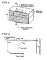
- FIGURE 1 illustrates a high voltage Schottky barrier diode 10 in accordance with our invention.
- Diode 10 includes a body 12 having a substrate layer 14, preferably comprising gallium arsenide, and a voltage-supporting layer 16 of gallium arsenide thereon. Layers 14 and 16 preferably contain N-type dopant impurities, as illustrated.
- Diode 10 further includes a first electrode 18, which adjoins voltage-supporting layer 16 and forms a Schottky barrier rectifying contact therewith, and a second electrode 20, which adjoins substrate layer 14 and forms a non-rectifying or obmic contact therewith.
- First and second electrodes 18 and 20 are suitably applied to semiconductor body 12 by the known technique of shadow evaporation.
- electrode 18 preferably comprises tungsten which has been annealed at a temperature in excess of about 450°C for longer than about 60 minutes.
- a material such as aluminum (not shown) to which leads can be readily soldered is advantageously formed over first electrode 18 to facilitate contact to an external circuit (not shown).
- Substrate 14 has a high dopant concentration,e.g., 10 18 impurity atoms per cubic centimeter, so as to form an ohmic contact with second electrode 20 which is attached thereto.
- Substrate 14 preferably has a (111) crystallographic orientation, although substrates with other orientations can alternatively be used.
- Voltage-supporting layer 16 of gallium arsenide preferably comprises an epitaxial layer grown, for example, by either the vapor-phase technique or the liquid-phase technique.
- Such techniques are described in details, for example, in a collection of articles complied in David J. Colliver, Compound Semiconductor Technology, Dedham, Massachusetts: Artech House, Inc. (1976) pages 8-40.
- the dopant concentration of voltage-supporting layer 16 is less than about 10 impurity atoms per cubic centimeter.
- diode 10 can block current at reverse voltages up to nearly its ideal reverse breakdown voltage and that it exhibits extremely low reverse leakage current up to its reverse breakdown voltage, at least where first electrode 18 comprises tungsten annealed as described above, or gold.
- diode 10 attains these advantages without requiring any special structure for terminating edge 22 of first electrode 18 upon voltage-supporting layer 16, in contradistinction to a high voltage Schottky diode comprising silicon.
- diode 10 With reverse breakdown voltages up to 600 volts, and would appear to hold true for diode 10 with higher reverse breakdown voltages. These findings indicate that diode 10 does not suffer from the effects of a high electric field gradient at contrary to edge 22 of first electrode 18,/what the prior art suggests. We have also found that diode 10 operates unimpaired at high temperatures up to at least 300°C, at least where first electrode 18 comprises tungsten annealed as described above.
- Reverse characteristic 50 is for a particular gallium arsenide diode having an ideal reverse breakdown voltage of 200 volts
- reverse characteristic 52 is for a typical prior art, high voltage, silicon Schottky barrier diode, likewise having an ideal reverse breakdown voltage of 200 volts the characteristics 50 and 52 being measured with both diodes at a temperature of 100°C.
- the data for reverse characteristic 52 is taken from FIGURE 10 of the above-referenced article of L.F.Cordes and M. Garfinkel.
- gallium arsenide diode 10 of FIGURE 1 possess the advantages discussed in relation to FIGURE 2, but it also possesses the highly desirable advantage of having low resistance, allowing it to carry about 12 times as much current as a silicon diode, or to be made about one-twelfth the size of a silicon diode, for devices with the same reverse breakdown voltages and forward voltage drops.
- gallium arsenide diode 10 Further details of construction of high voltage, gallium arsenide diode 10 are contained in the following articles which were written on our behalf to describe aspects of our invention: B.J. Baliga et al, "Breakdown Characteristics of Gallium Arsenide," IEEE Transactions; Electron Device Letters, Vol. EDL-2, No.ll (November 1981) pages 302-304; B.J. Baliga et al., "Breakdown Stability of Gold Aluminum, and Tungsten Schottky Barriers on Gallium Arsenide," IEEE Electron Device Letters, Vol. EDL-3, No. 7, (July 1982), pages 177-179.
- the disclosures of the foregoing articles are incorporated herein in their entireties by reference.
Landscapes
- Electrodes Of Semiconductors (AREA)
Applications Claiming Priority (2)
| Application Number | Priority Date | Filing Date | Title |
|---|---|---|---|
| US41985282A | 1982-09-20 | 1982-09-20 | |
| US419852 | 1982-09-20 |
Publications (2)
| Publication Number | Publication Date |
|---|---|
| EP0106072A2 true EP0106072A2 (de) | 1984-04-25 |
| EP0106072A3 EP0106072A3 (de) | 1985-07-03 |
Family
ID=23664029
Family Applications (1)
| Application Number | Title | Priority Date | Filing Date |
|---|---|---|---|
| EP83108283A Withdrawn EP0106072A3 (de) | 1982-09-20 | 1983-08-23 | Hochspannungs-Schottky-Diode |
Country Status (2)
| Country | Link |
|---|---|
| EP (1) | EP0106072A3 (de) |
| JP (1) | JPS5976479A (de) |
Family Cites Families (1)
| Publication number | Priority date | Publication date | Assignee | Title |
|---|---|---|---|---|
| GB1495188A (en) * | 1974-09-14 | 1977-12-14 | Tokyo Shibaura Electric Co | Method for manufacturing a semiconductor device |
-
1983
- 1983-08-23 EP EP83108283A patent/EP0106072A3/de not_active Withdrawn
- 1983-09-16 JP JP58169496A patent/JPS5976479A/ja active Pending
Also Published As
| Publication number | Publication date |
|---|---|
| EP0106072A3 (de) | 1985-07-03 |
| JPS5976479A (ja) | 1984-05-01 |
Similar Documents
| Publication | Publication Date | Title |
|---|---|---|
| USRE49167E1 (en) | Passivation structure for semiconductor devices | |
| Bhatnagar et al. | Silicon-carbide high-voltage (400 V) Schottky barrier diodes | |
| US5539217A (en) | Silicon carbide thyristor | |
| US8952481B2 (en) | Super surge diodes | |
| Cooper et al. | SiC power-switching devices-the second electronics revolution? | |
| US8445917B2 (en) | Bidirectional silicon carbide transient voltage suppression devices | |
| US4110775A (en) | Schottky diode with voltage limiting guard band | |
| US7586156B2 (en) | Wide bandgap device in parallel with a device that has a lower avalanche breakdown voltage and a higher forward voltage drop than the wide bandgap device | |
| US4075650A (en) | Millimeter wave semiconductor device | |
| US2983854A (en) | Semiconductive device | |
| Hull et al. | Development of large area (up to 1.5 cm2) 4h-sic 10 kv junction barrier schottky rectifiers | |
| US4053924A (en) | Ion-implanted semiconductor abrupt junction | |
| EP0163031B1 (de) | Supraleitender Transistor | |
| Irokawa et al. | Current–voltage and reverse recovery characteristics of bulk GaN pin rectifiers | |
| Agarwal et al. | 4H–SiC p–n diodes and gate turnoff thyristors for high-power, high-temperature applications | |
| Das et al. | Ultra high power 10 kV, 50 A SiC PiN diodes | |
| US3308356A (en) | Silicon carbide semiconductor device | |
| EP0106072A2 (de) | Hochspannungs-Schottky-Diode | |
| US3248614A (en) | Formation of small area junction devices | |
| US7615801B2 (en) | High voltage silicon carbide devices having bi-directional blocking capabilities | |
| WO1995034915A1 (en) | Semiconductor device in silicon carbide | |
| US3649890A (en) | High burnout resistance schottky barrier diode | |
| Chang et al. | High-current, low-forward-drop JBS power rectifiers | |
| Irvin et al. | Nonohmic contacts for microwave devices | |
| Ortolland | Study of different edge terminations used for 6H-SiC power diodes |
Legal Events
| Date | Code | Title | Description |
|---|---|---|---|
| PUAI | Public reference made under article 153(3) epc to a published international application that has entered the european phase |
Free format text: ORIGINAL CODE: 0009012 |
|
| AK | Designated contracting states |
Designated state(s): DE FR GB NL |
|
| PUAL | Search report despatched |
Free format text: ORIGINAL CODE: 0009013 |
|
| AK | Designated contracting states |
Designated state(s): DE FR GB NL |
|
| 17P | Request for examination filed |
Effective date: 19851228 |
|
| 17Q | First examination report despatched |
Effective date: 19861124 |
|
| STAA | Information on the status of an ep patent application or granted ep patent |
Free format text: STATUS: THE APPLICATION IS DEEMED TO BE WITHDRAWN |
|
| 18D | Application deemed to be withdrawn |
Effective date: 19870604 |
|
| RIN1 | Information on inventor provided before grant (corrected) |
Inventor name: ADLER, MICHAEL STUART Inventor name: BALIGA, BANTVAL JAYANT |