EP0104763B1 - An electron beam pattern transfer system having an autofocusing mechanism - Google Patents
An electron beam pattern transfer system having an autofocusing mechanism Download PDFInfo
- Publication number
- EP0104763B1 EP0104763B1 EP83304870A EP83304870A EP0104763B1 EP 0104763 B1 EP0104763 B1 EP 0104763B1 EP 83304870 A EP83304870 A EP 83304870A EP 83304870 A EP83304870 A EP 83304870A EP 0104763 B1 EP0104763 B1 EP 0104763B1
- Authority
- EP
- European Patent Office
- Prior art keywords
- mask
- substrate
- magnetic field
- difference
- detecting
- Prior art date
- Legal status (The legal status is an assumption and is not a legal conclusion. Google has not performed a legal analysis and makes no representation as to the accuracy of the status listed.)
- Expired
Links
Images

Classifications
-
- B—PERFORMING OPERATIONS; TRANSPORTING
- B82—NANOTECHNOLOGY
- B82Y—SPECIFIC USES OR APPLICATIONS OF NANOSTRUCTURES; MEASUREMENT OR ANALYSIS OF NANOSTRUCTURES; MANUFACTURE OR TREATMENT OF NANOSTRUCTURES
- B82Y10/00—Nanotechnology for information processing, storage or transmission, e.g. quantum computing or single electron logic
-
- H—ELECTRICITY
- H01—ELECTRIC ELEMENTS
- H01J—ELECTRIC DISCHARGE TUBES OR DISCHARGE LAMPS
- H01J37/00—Discharge tubes with provision for introducing objects or material to be exposed to the discharge, e.g. for the purpose of examination or processing thereof
- H01J37/02—Details
- H01J37/21—Means for adjusting the focus
-
- B—PERFORMING OPERATIONS; TRANSPORTING
- B82—NANOTECHNOLOGY
- B82Y—SPECIFIC USES OR APPLICATIONS OF NANOSTRUCTURES; MEASUREMENT OR ANALYSIS OF NANOSTRUCTURES; MANUFACTURE OR TREATMENT OF NANOSTRUCTURES
- B82Y40/00—Manufacture or treatment of nanostructures
-
- H—ELECTRICITY
- H01—ELECTRIC ELEMENTS
- H01J—ELECTRIC DISCHARGE TUBES OR DISCHARGE LAMPS
- H01J37/00—Discharge tubes with provision for introducing objects or material to be exposed to the discharge, e.g. for the purpose of examination or processing thereof
- H01J37/30—Electron-beam or ion-beam tubes for localised treatment of objects
- H01J37/304—Controlling tubes by information coming from the objects or from the beam, e.g. correction signals
-
- H—ELECTRICITY
- H01—ELECTRIC ELEMENTS
- H01J—ELECTRIC DISCHARGE TUBES OR DISCHARGE LAMPS
- H01J37/00—Discharge tubes with provision for introducing objects or material to be exposed to the discharge, e.g. for the purpose of examination or processing thereof
- H01J37/30—Electron-beam or ion-beam tubes for localised treatment of objects
- H01J37/317—Electron-beam or ion-beam tubes for localised treatment of objects for changing properties of the objects or for applying thin layers thereon, e.g. for ion implantation
- H01J37/3174—Particle-beam lithography, e.g. electron beam lithography
- H01J37/3175—Projection methods, i.e. transfer substantially complete pattern to substrate
-
- H—ELECTRICITY
- H01—ELECTRIC ELEMENTS
- H01J—ELECTRIC DISCHARGE TUBES OR DISCHARGE LAMPS
- H01J2237/00—Discharge tubes exposing object to beam, e.g. for analysis treatment, etching, imaging
- H01J2237/21—Focus adjustment
- H01J2237/216—Automatic focusing methods
-
- H—ELECTRICITY
- H01—ELECTRIC ELEMENTS
- H01J—ELECTRIC DISCHARGE TUBES OR DISCHARGE LAMPS
- H01J2237/00—Discharge tubes exposing object to beam, e.g. for analysis treatment, etching, imaging
- H01J2237/30—Electron or ion beam tubes for processing objects
- H01J2237/304—Controlling tubes
- H01J2237/30455—Correction during exposure
-
- H—ELECTRICITY
- H01—ELECTRIC ELEMENTS
- H01J—ELECTRIC DISCHARGE TUBES OR DISCHARGE LAMPS
- H01J2237/00—Discharge tubes exposing object to beam, e.g. for analysis treatment, etching, imaging
- H01J2237/30—Electron or ion beam tubes for processing objects
- H01J2237/317—Processing objects on a microscale
- H01J2237/3175—Lithography
- H01J2237/31777—Lithography by projection
- H01J2237/31779—Lithography by projection from patterned photocathode
-
- Y—GENERAL TAGGING OF NEW TECHNOLOGICAL DEVELOPMENTS; GENERAL TAGGING OF CROSS-SECTIONAL TECHNOLOGIES SPANNING OVER SEVERAL SECTIONS OF THE IPC; TECHNICAL SUBJECTS COVERED BY FORMER USPC CROSS-REFERENCE ART COLLECTIONS [XRACs] AND DIGESTS
- Y10—TECHNICAL SUBJECTS COVERED BY FORMER USPC
- Y10S—TECHNICAL SUBJECTS COVERED BY FORMER USPC CROSS-REFERENCE ART COLLECTIONS [XRACs] AND DIGESTS
- Y10S505/00—Superconductor technology: apparatus, material, process
- Y10S505/825—Apparatus per se, device per se, or process of making or operating same
- Y10S505/879—Magnet or electromagnet
Definitions
- This invention relates to an electron beam pattern transfer system using a photoelectric transducing mask.
- a pattern transfer system utilizing an X-ray or an electron beam instead of a light beam shows promise as a new ultrafine patterning technique.
- an ultraviolet ray is directed onto a photoelectrical transducing mask which is positioned parallel to a substrate such as a semiconductor wafer and under uniform, strong electric and magnetic fields created between the mask and the substrate a photoelectron beam pattern is focused onto a resist film on the wafer so as to transfer a mask pattern onto the resist film on the wafer.
- This system permits the transfer of an ultrafine pattern onto a submicron area.
- the patterning technique of this kind has various advantages including, for example, the following: (1) a high-speed pattern transfer can be carried out with a high yield; and (2) since the mask is similar in structure to a photomask, the conventional technique can be used in the fabrication of the mask structure.
- this electron beam pattern transfer system involves the following problem with respect to the wafer alignment technique.
- the photoelectron beam pattern emitted from the photoelectric surface of the mask is focused onto a silicon wafer, and an acceleration voltage V is applied between the mask and the wafer, focusing magnetic field intensity B and mask-to-wafer distance d are important parameters.
- V acceleration voltage
- focusing magnetic field intensity B and mask-to-wafer distance d are important parameters.
- a deviation of the applied voltage V from a set value should be reduced to below 0.02% and a variation in the focusing magnetic field intensity B should be reduced to below 0.01 %.
- An article entitled Electron-Image Projector by J. P. Scott, Phillips Technical Review 37, 347-356, 1977, No. 11/12 discloses an electron-image projector in which a mask M is placed in an evacuated chamber some distance from a silicon slice on which an IC is to be produced. The slice is coated with an electron-sensitive resist. Both mask and slice are situated in a magnetic field and a high voltage is connected between the mask and the slice. When the mask is illuminated with ultra-violet light, this causes electrons to be emitted from the photo-emitter behind the clear parts of the mask but not from the opaque regions thereof. The electrons are accelerated by the electric field and focused by the combination of magnetic and electric fields so as to produce an accurate image of the clear areas of mask on the substrate so that the pattern is transferred from the mask to the silicon slice.
- an apparatus for transferring a desired fine pattern onto a target body, such as a substrate having a resist film, by the use of electron beam having container means for defining a transfer chamber which is evacuated to a predetermined vacuum level, photoelectrical transducing mask means provided in the transfer chamber and arranged in a spaced-apart relation to the substrate, having a pattern to be transferred onto the resist film of the substrate and adapted to receive light to permit a photoelectron beam pattern corresponding to the pattern of the mask means to be emitted onto the resist film, table means movably provided in the transfer chamber to support the substrate thereon, magnetic field generating means positioned around said container means, for generating a magnetic field of a predetermined intensity in a space between the mask means and the substrate in said transfer chamber, and voltage generator means provided outside said container means, for applying a DC voltage between the mask means and the substrate to create an electric field therebetween, characterised in that said apparatus comprises: defocus detector means for, when an electron beam pattern image is formed on the
- a new and improved electron beam transfer system may be provided which can properly and automatically adjust the focusing of an electron beam pattern onto a target body (sample) such as a resist film on a substrate and can transfer the pattern to the resist film with high image resolution.
- a variation in the distance between a photoelectrical transducing mask and a target body onto which an electron beam pattern corresponding to mask pattern is directed, and/or a variation in the intensity of a magnetic field created between the target body and the mask are quantitatively detected.
- the focusing mechanism automatically eliminates any amount of defocusing which occurs due to variations in the above-mentioned parameters by correcting the intensity of an electric field which is created between the mask and the target body. That is, the focusing mechanism automatically detects the variation in the parameters and calculates the necessary amount of correction of the electric field intensity to compensate for the detected amount of variation, on a real-time basis.
- a voltage generator permits a mask-to-target body voltage to vary in response to a signal corresponding to a calculated amount.
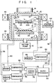
- FIG. 1 shows an electron beam pattern transfer system according to one embodiment of this invention.
- a cylindrical container 10 has an opening 12 at the top wall.
- the opening 12 is hermetically closed by a plate 14 made of a material, such as quartz, which permits the passage of an ultra- violet ray emitted from an external light source 16.
- the container 10 is coupled at its bottom to a vacuum pump 18 to evacuate an inner space, i.e., a transfer chamber 10a in the container 10, to a vacuum level of, for example, 133 pPa (10- 6 Torr).
- a mask 20 is located substantially parallel to and at a reference distance of, for example, 10 mm from a table 22 and in the axial direction of the container 10.
- a target body or sample 24 made of a substrative body, such as a silicon wafer or a glass (quartz) substrate, is placed on the table 22.
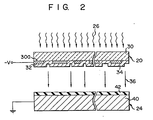
- the mask 20 comprises a glass substrate 30 for permitting the effective passage of ultraviolet rays 26 radiated from the light source 16 (Fig. 1), a mask pattern layer 32 formed in a desired pattern on the transparent substrate 30 and made of an ultra- violet-absorbing material, and a photoelectric layer 34 deposited on the substrate 30 and mask pattern layer 32 and made of Csl to permit a photoelectron beam 36 to be emitted in a manner corresponding to the ultraviolet rays 26 entering the photoelectric layer 34 through the substrate 30.
- the photoelectric layer 34 faces the sample (target body) and is illuminated with ultraviolet rays 26 emitted from the source 16 and transmitted through the transparent substrate 30, that light portion incident on the mask pattern layer 32 being absorbed therein.
- the photoelectron beam 36 emitted from the layer 30 of the mask 20 forms an electron beam pattern corresponding to the configuration of a mask pattern and is directed onto the sample 24 on the table 22 within the vacuum container 10.
- the sample 24 may be a monocrystalline silicon wafer 40 on which an electron-sensitive resistfilm 42 is formed.
- This film 42 is made of, for example, polymethyl methacrylate (PMMA).
- the electron beam pattern 36 from the mask 20 is directed onto the electron-sensitive resist film 42 on the wafer 40 to permit the film 42 to be exposed.
- the electric field is created by applying a high DC voltage of, for example, about 20 KV between the mask 20 and the sample 24.
- the DC voltage is developed by an external DC voltage generator 44.
- the magnetic field is created between the mask 20 and the sample 24 by a pair of ring coils 46.
- the coils 46 are immovably mounted around the external peripheral wall of the vacuum container 10.
- a uniform vertical field is created from the mask 20 toward the sample 24. Since in this embodiment the acceleration voltage is set to 20 KV, a superconductive magnet is preferably utilized as a focusing coil 46 to stably and uniformly create a strong magnetic field having an intensity corresponding to the electric field intensity at this time.
- the superconductive magnet can produce a strong magnetic field since it permits the ready flow of a large current. It can also realize better uniformity of magnetic field by a simple magnet arrangement of a Helmholtz type, because it permits larger ring coil arrangement.
- a permanent current mode i.e., a characteristic of the superconductive magnet, a magnetic field substantially free from any unstable factors, such as drift or ripple, can be formed between the mask 20 and the sample 24.
- the electron beam pattern 36 emitted from the mask 20 is focused onto the electron-sensitive resist film 42 on the wafer by the electric and magnetic fields created by the voltage generator 44 and superconductive magnet focusing coil 46.
- the electron-sensitive resist film 42 is exposed with the electron beam pattern 36 so that the mask pattern of the mask 20 is transferred to the sample 24.
- the relation among (i) a mask-to-sample distance d, (ii) the intensity of a magnetic field B, and (iii) a voltage V applied between the mask and the sample and defining the intensity of an electric field is properly determined by Equation (1) below: where m: the mass of the electron, e: the charge of the electron.
- a reference distance do between the mask and the sample was determined to be 10 mm and a reference voltage V o applied between the mask and the sample was set to 20 KV in the initial design as described above.
- a reference focusing magnetic field intensity B o was determined to be 0.14 T (1.4 KG).
- the electron beam pattern transfer system of this invention includes an automatic focus-correcting mechanism, which will be described below.
- an optical distance measuring device is set within the vacuum transfer chamber 10a.
- the distance measuring device is comprised of a light emitting element 50 and light receiving element 52 for measuring the actual position of the mask 20, and a light emitting element 54 and light receiving element 56 for measuring the actual position of the sample 24.
- the pair of these elements 50, 52 are arranged such that, in orderto accurately detect the position of the mask pattern layer 32 on the transparent substrate 30, the element 52 is adapted to receive the light beam components which are reflected at the junction face 30a between the substrate 30 and the mask pattern layer 32 after light is emitted from the element 50.
- Electrical detection signals 58 and 60 representing the actual mask position and sample position, respectively, are produced from the elements 52 and 56.
- the detection signals 58 and 60 are supplied to first and second comparators 64 and 66 of a distance error detector 62.
- the first comparator 64 is adapted to detect a deviation from an initially set reference position and has a first input terminal connected to a memory 68, such as a ROM, provided in the detector 62 to store the reference position data of the mask and a second input terminal for receiving the detection signal 58.
- the comparator 64 compares the signal 58 and the reference position data from the memory 68 to produce a comparison result signal 70 corresponding to the difference (L1d1) therebetween.
- the signal 70 contains a sign (plus or minus) and represents the difference between the actual position data, which are represented by the signal 58, and reference position data.
- the second comparator 66 is adapted to detect a deviation from an initially set reference position of the mask (In this connection it is evident that the above-mentioned reference distance do is defined by the reference positions of the mask 20 and sample 24.), and has a first input terminal connected to a memory 72 provided in the detector 62 to store the reference position data from the memory 72 and a second input terminal for receiving the detection signal 60.
- the comparator 66 compares the signal 60 with the data from the memory 72 to produce a comparison result signal 74 corresponding to the difference (L1d2) under the same name as that in the first comparator 64.
- the first and second comparators 64 and 66 have their output terminals connected to an adding circuit 76 in the detector 62.
- the adding circuit 76 is adapted to additively process the distance deviation data Lld1 and Ad 2 from the comparators 64 and 66 to produce addition result data as an electrical signal 78 which represents a deviation of the actual mask-to-sample distance d from the reference distance do.
- a magnetic field intensity measuring system such as a Hall element 80, is hermetically sealed within the transfer chamber 10a of the vacuum container 10 to measure the actual intensity of the magnetic field B, which is created by the superconductive magnet coils 46 within the transfer chamber 10a.
- the Hall element 80 is adapted to supply an electrical signal 84 representing the actual intensity of the magnetic field within the transfer chamber 10a to a magnetic field intensity error detector 82.
- the detector 82 includes a memory 86 for storing the reference magnetic field intensity data B o and a comparator (third comparator) 84 having a first input terminal connected to the memory 86 and a second input terminal to which the signal 84 representing the actual magnetic field intensity B is supplied from the Hall element 80.
- the comparator 84 delivers, as a magnetic field intensity error AB, a comparison result signal 88 corresponding to difference data between the input signals of the memory 86 and Hall element 80.
- the error signals 78 and 88 of the circuits 62 and 82 are conveyed to a control unit 90 having a microprocessor.
- a voltage V is calculated based on the following equation and calculation result data is supplied, as the control signal 92, to the DC voltage generator 44.
- k is a constant.
- the DC voltage generator 44 permits its output voltage to vary in response to the signal 92.
- the voltage applied between the mask 20 and the sample 24 is corrected by an amount AV. Consequently, the mask-to-sample voltage varies in proportion to the corrected voltage, permitting focusing the electron beam pattern onto the sample 24.
- the mask-to-sample voltage V is corrected and thus the electron beam pattern from the mask is accurately focused onto the sample 24, causing the electron beam pattern to be transferred onto the sample with a high image resolution.
- the correction of the mask-to-sample voltage applied can be effected using real-time processing without a delay.
- the pattern transfer operation can be effectively performed, while always maintaining a good image resolution, and a high yield can be obtained in the pattern transfer operation.
- the mask 20 or the sample 24 i.e., the silicon wafer 40 with the resist film 42
- the mask 20 or the sample 24 i.e., the silicon wafer 40 with the resist film 42
- One correction method may be considered which mechanically adjusts the height of the table 22 so as to adjust the variation of this distance on the order of a micron unit.
- Such mechanical method is still inadequate. According to the system of Fig.
- the variation or deviation of the mask-to-sample distance is electrically detected by the optical detecting meane(50, 52, 54, 56) and detector 62 and an error compensation processing is carried out by the microprocessor 90 on a real-time basis.
- the voltage generator 44 corrects the output voltage applied between the mask 20 and the sample 24 in response to the control signal 92 from the microprocessor 90. Since the mask-to-sample electric field intensity B is properly corrected, the defocusing of the electron beam resulting from the error components of the distance d can be corrected on a real-time basis.
- the superconductive magnet coil used as the focusing magnet 46 is driven in a permanent current mode, preventing a variation in the magnetic field created due to a variation of a power source voltage level and/or the application of ripple components to obtain a stable, uniform magnetic field.
- the current flowing through the superconductive magnet coil 46 will be unavoidably decreased due to long term usage. It is generally necessary that, in order to correct the defocusing of the electron beam on the sample 24 due to a decrease in the magnetic field intensity resulting from the decrease in the current, the permanent current mode of the superconductive magnet coil 46 must be interrupted once and a normal current must be used instead.
- the current-adjusting operation of the superconductive magnet coil 46 is very cumbersome and time-consuming.
- the defocusing of the electron beam due to the decrease in the intensity of the magnetic field can be corrected quickly and effectively without requiring any cumbersome operation. This is because the decrease of the magnetic field intensity resulting from the decrease in the current of the superconductive magnet coil 46 is detected by the magnetic field intensity error detector 82 and the defocusing of the electron beam can be readily and correctly compensated for by varying the intensity of the mask-to-sample electric field by the control signal 92 from the microprocessor 90.
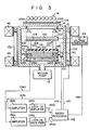
- Fig. 3 illustrates an electron beam pattern transfer system according to another embodiment of this invention.
- An X-ray detector is additionally provided for detecting X-rays generated according to an electron beam which is directed onto the sample.
- the waveform of a detection signal from the X-ray detector varies dependent upon the amount of focusing of the electron beam which is directed onto the sample.
- the proper focusing of the electron beam onto the sample can be effected by adjusting a mask-to-sample electric or magnetic field on the basis of the detection signal waveform data.
- a photoelectric transducing mask 100 is disposed in a vacuum container 10.
- the mask 100 is comprised of, like the mask 20 of Fig. 1, a quartz substrate 102, mask pattern layer 104 and photoelectric layer 106.
- the mask 100 has a special mask pattern 104' around the marginal edge area (P i , P 2 ) of the substrate 102 which pattern serves as an alignment mask pattern.
- the mask pattern 104' is different in its function from the mask pattern layer 104 corresponding to a circuit pattern to be transferred later onto a substrate or sample 110 and is adapted to generate an alignment electron beam to be used only for positional alignment between the mask 100 and the sample 110.
- a mechanical shutter 108 is provided between a light source 16 and a transparent plate 14 attached to a top window 12 of the vacuum container 10, so as to control the passage of an ultraviolet ray radiated from the light source 16.
- the shutter 108 closes the top window of the container except for openings 109a and 109b as shown in Fig. 3 to permit the ultraviolet ray to be directed onto that area of the mask pattern 104' for positional alignment.
- the shutter 108 is driven by a driver (not shown), causing it to be substantially fully opened to permit the ultraviolet ray to be directed to the whole area of the mask 100.
- the sample 110 is placed on a table structure 112 in the vacuum container 10.
- the sample 110 comprises a monocrystalline silicon substrate of wafer 114 and an electron sensitive resist film 116 such as PMMA is deposited on the wafer 114.
- Electron beam detection marks 118a and 118b for alignment are additionally provided on the marginal edge areas P 1 and P 2 of the silicon substrate 114 ofthe sample 110, respectively.
- the detection marks 118a and 118b have a pattern configuration corresponding to the mask patterns 104' formed on the marginal edge areas P 1 and P 2 of the mask 100, respectively.
- Each of the detection marks 118a and 118b is adapted to generate an X-ray according to an amount of electron beam illuminated and is made of a heavy metal, such as molybdenum or tantalum, which provides a better X-ray generation contrast characteristic between the mark 118a, b and the surface of the sample.
- a heavy metal such as molybdenum or tantalum
- the intensity of the X-ray which is generated from the metal depends upon the atomic number of the metal used as the mark. The intensity of, for example, a continuous X-ray is increased substantially proportional to the atomic number of the metal.
- tantalum (Ta) is preferably selected as the heavy metal for the marks 118a and 118b.
- an electron beam for alignment which is indicated by 120 in Fig. 3 is generated therefrom.
- the electron beam 120 is introduced from the mask 100 onto the corresponding marginal edge area of the sample 110.
- the table structure 112 includes a supporting body 122 which has two openings 124a and 124b corresponding to the marginal edge areas P, and P 2 of the mask 100 or the detection marks 118a and 118b of the sample 110.
- Two X-ray detectors 126a and 126b are housed in the openings 124a and 124b, respectively, and adapted to detect an X-ray which is generated from the marks 118a and 118b of the sample 110 due to the illumination of the mask 100 with the ultraviolet ray.
- a base 128 of the supporting body 122 is rotatable through a desired angle in an X-Y plane by a table rotation driver 130, permitting the sample 110 on the supporting body 122 to be rotated a necessary amount.
- reference numeral 132 denotes an X- and Y-deflection coil for deflecting an electron beam in the X- and Y-directions.
- Detection signals 134a and 134b generated from the detectors 126a and 126b are supplied to signal amplifiers 136a and 136b, respectively, of, for example, a photomultiplier.
- the outputs of the amplifiers 136a and 136b are connected respectively through lock-in amplifiers 138a and 138b to a control section or microprocessor 142.
- Each of the lock-in amplifiers 138a and 138b detects the envelope waveform of the detection signal 134, followed by a differential amplification (a lock-in detection amplification).
- the control section comprised of the microprocessor 142 supplies control signals 144, 145 and 146 to the table rotation driver 130, deflection coil 132 and DC voltage generator 44 in response to output signals 140a and 140b from the lock-in amplifiers 138a and 138b.
- the accelerated electron beam while being deflected in the X- and/or Y-direction by the deflection coil 132, bombards the heavy metal area of the detection marks 118a and 118b of the sample 110.
- the marks 118a and 118b generate an X-ray as set out above.
- the X-ray enters through the silicon wafer 114 of the sample 110 into the X-ray detectors 126a and 126b held in the table structure 112.
- the X-ray detectors 126a and 126b produce the detection signals 134a and 134b according to the intensity of the incident X-ray.
- the level intensity I of the detection signal 134 from the X-ray detector 126 varies, in a quadratic curve, dependent upon the mask pattern-to-sample displacement AdX (or AdY) in the X- or Y-direction.
- the level intensity I of the detection signal 134 has a peak value I P as indicated by lp in Fig.
- the detection signal having such characteristic is amplified by the lock-in amplifier 138 to deliver a signal 140 having a substantially differentiated waveform as shown in Fig. 4B.
- the detection signal level I has a peak value lp
- the microprocessor 142 controls the deflection coil 132 in response to the signal 140 so as to permit the photoelectron beam directed from the mask 100 to the sample 110 to obtain an optimal magnetic deflection in the X- and Y-directions.
- the rotational displacement ⁇ O of the sample 110 is corrected by rotating the table structure 112 by the table rotation driver 130 under the control of the microprocessor 142.
- the photoelectron beam 120 is not properly focused onto the sample 110, causing the blur of the beam spot.
- the microprocessor 142 controls the DC voltage generator 44 so as to vary the mask-to-sample field effect intensity.
- the output signals 140a and 140b from the lock-in amplifiers 138a and 138b vary as indicated by 160, 162 in Fig. 5B.
- the microprocessor 142 decides that a best beam focusing is obtained, and sets the voltage value of the DC voltage generator to a value at that time. Thereafter, the shutter 108 is fully opened and a main step of pattern transfer can be started under the optimal condition.
- such automatic focus- correcting mechanism which adjusts the focusing of the electron beam onto the sample or workpiece 110 by utilizing the phenomenon that the detection signal waveform from the X-ray detector varies according to an amount of beam defocus on the sample 110. It is therefore unnecessary to precisely set the mask-to-sample distance. It is also unnecessary to perform any cumbersome operation, such as the measurement of the mask-to-sample distance and measurement of the actual magnetic field. Even if the position of the sample is displaced beyond the depth of focusing, an automatic beam focusing adjustment can be made, obviating the necessity of positioning the sample for vertical alignment. Even under the varying transfer conditions, the beam focusing adjustment can be readily performed without finding the corresponding focusing conditions. It is therefore possible to shorten the necessary setup time. For example, even under the varying transfer conditions a rapid beam focusing adjustment can be made without lowering the productivity.
- a laser interferometer may be used as a means for detecting a distance between the mask and the sample.
- the magnetic field detector is not restricted to the Hall element. Any means may be used instead if it can detect the intensity of a magnetic field between the mask and the sample.
- the degree of beam focusing is detected by the X-ray from the mark 118 on the workpiece 110, a similar mark, however, may be provided on a sample supporting member (sample supporting base) or a pattern having a restricted area illuminated with the photoelectron beam may be provided on the sample or the supporting member.
- the pattern or mark may be a photoelectron beam responding means that emits a charged particle ray, such as a radiation ray or an electron beam.
- the photoelectron beam is deflected in the X- and Y-directions by the X- and Y-deflection coil 132 to obtain an alignment signal and photoelectron beam intensity signal.
- the same functions can be performed by separate deflection coils.
Description
- This invention relates to an electron beam pattern transfer system using a photoelectric transducing mask.
- It has been impossible heretofore to increase the packing density of semiconductor devices, even by employing currently available fine patterning techniques (e.g., photolithography), due to the dimensional limits of a pattern resulting from the wavelength of light used. Consequently, there has been a great demand for the development of an even finer patterning technique, such as a submicron patterning technique.
- A pattern transfer system utilizing an X-ray or an electron beam instead of a light beam shows promise as a new ultrafine patterning technique. According to the electron beam pattern transfer system, an ultraviolet ray is directed onto a photoelectrical transducing mask which is positioned parallel to a substrate such as a semiconductor wafer and under uniform, strong electric and magnetic fields created between the mask and the substrate a photoelectron beam pattern is focused onto a resist film on the wafer so as to transfer a mask pattern onto the resist film on the wafer. This system permits the transfer of an ultrafine pattern onto a submicron area. The patterning technique of this kind has various advantages including, for example, the following: (1) a high-speed pattern transfer can be carried out with a high yield; and (2) since the mask is similar in structure to a photomask, the conventional technique can be used in the fabrication of the mask structure.
- On the other hand, this electron beam pattern transfer system involves the following problem with respect to the wafer alignment technique. When the photoelectron beam pattern emitted from the photoelectric surface of the mask is focused onto a silicon wafer, and an acceleration voltage V is applied between the mask and the wafer, focusing magnetic field intensity B and mask-to-wafer distance d are important parameters. In order to obtain a high image resolution characteristic, it is necessary to reduce the edge blur of the photoelectron beam pattern on the wafer to a minimum. For example, in order to control the edge resolution of the electron beam pattern down to below 0.1 µm, a deviation of the applied voltage V from a set value should be reduced to below 0.02% and a variation in the focusing magnetic field intensity B should be reduced to below 0.01 %. It is also necessary to reduce a variation in the mask-to-wafer distance d to a very small value. However, there is a high probability that the above-mentioned distance d will vary undesirably due to, for example, the replacement of the silicon wafer (sample), the replacement of the mask, and the accuracy with which a table having the wafer placed thereon is mechanically moved. Even if the accuracy of the applied voltage V and magnetic field intensity B can be enhanced, the edge blur of the electron beam pattern is increased due to inaccurate setting of the mask-to-wafer distance d, resulting in a lowered image resolution. It is therefore difficult in the prior art technique to focus the photoelectron beam pattern onto the wafer with high accuracy by effectively adjusting the above-mentioned three important parameters: the applied voltage V, magnetic field intensity B and distance d.
- In the prior art technique, for example, in order to focus an electron beam pattern onto the wafer, a pattern transfer is initially carried out and the applied voltage V and magnetic field intensity B are adjusted, while observing the transferred pattern image, to obtain an optical requirement. It is therefore impossible to adequately compensate for a variation in the mask-to-wafer distance. Furthermore, a great deal of time is required for focusing the electron beam pattern onto the wafer, thus lowering the rate of operation. It is also impossible to detect and compensate for any defocusing which may occur after focusing has been carried out. This leads to the problem of low yield in the pattern transfer operation.
- An article entitled Electron-Image Projector by J. P. Scott, Phillips Technical Review 37, 347-356, 1977, No. 11/12 discloses an electron-image projector in which a mask M is placed in an evacuated chamber some distance from a silicon slice on which an IC is to be produced. The slice is coated with an electron-sensitive resist. Both mask and slice are situated in a magnetic field and a high voltage is connected between the mask and the slice. When the mask is illuminated with ultra-violet light, this causes electrons to be emitted from the photo-emitter behind the clear parts of the mask but not from the opaque regions thereof. The electrons are accelerated by the electric field and focused by the combination of magnetic and electric fields so as to produce an accurate image of the clear areas of mask on the substrate so that the pattern is transferred from the mask to the silicon slice.
- According to the invention, there is provided an apparatus for transferring a desired fine pattern onto a target body, such as a substrate having a resist film, by the use of electron beam, having container means for defining a transfer chamber which is evacuated to a predetermined vacuum level, photoelectrical transducing mask means provided in the transfer chamber and arranged in a spaced-apart relation to the substrate, having a pattern to be transferred onto the resist film of the substrate and adapted to receive light to permit a photoelectron beam pattern corresponding to the pattern of the mask means to be emitted onto the resist film, table means movably provided in the transfer chamber to support the substrate thereon, magnetic field generating means positioned around said container means, for generating a magnetic field of a predetermined intensity in a space between the mask means and the substrate in said transfer chamber, and voltage generator means provided outside said container means, for applying a DC voltage between the mask means and the substrate to create an electric field therebetween, characterised in that said apparatus comprises: defocus detector means for, when an electron beam pattern image is formed on the resist film of the substrate, automatically detecting the defocusing of the photoelectron beam pattern on the substrate by detecting a variation in the distance between the mask means and target body and/or a variation in the intensity of the magnetic field created between said mask means and target, and for producing a detection signal; and focusing controller means, connected to said voltage generator means and said defocus detector means, for controlling, in response to the detection signal, said voltage generator means so as to vary its output voltage and vary the electric field according to the amount of detected defocusing to compensate for said amount of defocusing, whereby said amount of defocusing is compensated for by controlling essentially only said voltage generator means.
- It is a believed possibility of this invention that a new and improved electron beam transfer system may be provided which can properly and automatically adjust the focusing of an electron beam pattern onto a target body (sample) such as a resist film on a substrate and can transfer the pattern to the resist film with high image resolution.
- In the described embodiments of this invention a variation in the distance between a photoelectrical transducing mask and a target body onto which an electron beam pattern corresponding to mask pattern is directed, and/or a variation in the intensity of a magnetic field created between the target body and the mask are quantitatively detected. The focusing mechanism automatically eliminates any amount of defocusing which occurs due to variations in the above-mentioned parameters by correcting the intensity of an electric field which is created between the mask and the target body. That is, the focusing mechanism automatically detects the variation in the parameters and calculates the necessary amount of correction of the electric field intensity to compensate for the detected amount of variation, on a real-time basis. A voltage generator permits a mask-to-target body voltage to vary in response to a signal corresponding to a calculated amount.
- Embodiments of the invention will now be described, by way of example, with reference to the accompanying drawings, in which:
- Fig. 1 is a block diagram schematically showing the whole structure of an electron beam pattern transfer system according to a preferred embodiment of this invention;
- Fig. 2 is a partially enlarged view showing a photoelectric transducing mask and a sample, i.e., a silicon wafer with a photoresist film, which are placed in a vacuum transfer chamber of the electron beam pattern transfer system of Fig. 1;
- Fig. 3 is a block diagram schematically showing the whole structure of an electron beam pattern transfer system according to another embodiment of this invention;
- Fig. 4A is a graph showing the variation of a detection signal output from the X-ray detector of the system of Fig. 3, with respect to the .deflection of an electron beam in an X or Y direction;
- Fig. 4B is a graph showing the waveform of an output signal from a lock-in amplifier of Fig. 3, the waveform corresponding to a differentiation waveform of Fig. 4A; and
- Figs. 5A and 5B are graphs showing the degree with which the electron beam is focused on a workpiece, the graphs corresponding to the waveforms of Figs. 4A and 4B.
- Fig. 1 shows an electron beam pattern transfer system according to one embodiment of this invention. A
cylindrical container 10 has anopening 12 at the top wall. Theopening 12 is hermetically closed by aplate 14 made of a material, such as quartz, which permits the passage of an ultra- violet ray emitted from anexternal light source 16. Thecontainer 10 is coupled at its bottom to avacuum pump 18 to evacuate an inner space, i.e., a transfer chamber 10a in thecontainer 10, to a vacuum level of, for example, 133 pPa (10-6 Torr). Within thecontainer 10, amask 20 is located substantially parallel to and at a reference distance of, for example, 10 mm from a table 22 and in the axial direction of thecontainer 10. A target body orsample 24 made of a substrative body, such as a silicon wafer or a glass (quartz) substrate, is placed on the table 22. - As shown more clearly in Fig. 2, the
mask 20 comprises aglass substrate 30 for permitting the effective passage ofultraviolet rays 26 radiated from the light source 16 (Fig. 1), amask pattern layer 32 formed in a desired pattern on thetransparent substrate 30 and made of an ultra- violet-absorbing material, and aphotoelectric layer 34 deposited on thesubstrate 30 andmask pattern layer 32 and made of Csl to permit aphotoelectron beam 36 to be emitted in a manner corresponding to theultraviolet rays 26 entering thephotoelectric layer 34 through thesubstrate 30. Thephotoelectric layer 34 faces the sample (target body) and is illuminated withultraviolet rays 26 emitted from thesource 16 and transmitted through thetransparent substrate 30, that light portion incident on themask pattern layer 32 being absorbed therein. Thephotoelectron beam 36 emitted from thelayer 30 of themask 20 forms an electron beam pattern corresponding to the configuration of a mask pattern and is directed onto thesample 24 on the table 22 within thevacuum container 10. - The
sample 24 may be a monocrystalline silicon wafer 40 on which an electron-sensitive resistfilm 42 is formed. Thisfilm 42 is made of, for example, polymethyl methacrylate (PMMA). - The
electron beam pattern 36 from themask 20 is directed onto the electron-sensitive resist film 42 on thewafer 40 to permit thefilm 42 to be exposed. Between themask 20 and thesample 24 theelectron beam pattern 36 is accelerated and focused by both an electric and a magnetic field. The electric field is created by applying a high DC voltage of, for example, about 20 KV between themask 20 and thesample 24. The DC voltage is developed by an externalDC voltage generator 44. When the voltage is applied, themask 20 is held at a negative voltage level -V (V=20 KV, for example) with thewafer 40 grounded as shown in Fig. 2. The magnetic field is created between themask 20 and thesample 24 by a pair ofring coils 46. Thecoils 46 are immovably mounted around the external peripheral wall of thevacuum container 10. Within the transfer chamber 10a, a uniform vertical field is created from themask 20 toward thesample 24. Since in this embodiment the acceleration voltage is set to 20 KV, a superconductive magnet is preferably utilized as a focusingcoil 46 to stably and uniformly create a strong magnetic field having an intensity corresponding to the electric field intensity at this time. The superconductive magnet can produce a strong magnetic field since it permits the ready flow of a large current. It can also realize better uniformity of magnetic field by a simple magnet arrangement of a Helmholtz type, because it permits larger ring coil arrangement. By using a permanent current mode, i.e., a characteristic of the superconductive magnet, a magnetic field substantially free from any unstable factors, such as drift or ripple, can be formed between themask 20 and thesample 24. - The
electron beam pattern 36 emitted from themask 20 is focused onto the electron-sensitive resistfilm 42 on the wafer by the electric and magnetic fields created by thevoltage generator 44 and superconductivemagnet focusing coil 46. As a result, the electron-sensitive resistfilm 42 is exposed with theelectron beam pattern 36 so that the mask pattern of themask 20 is transferred to thesample 24. In order to correctly focus the electron beam pattern onto thesample 24 with the best possible resolution, the relation among (i) a mask-to-sample distance d, (ii) the intensity of a magnetic field B, and (iii) a voltage V applied between the mask and the sample and defining the intensity of an electric field is properly determined by Equation (1) below:
- According to this embodiment, a reference distance do between the mask and the sample was determined to be 10 mm and a reference voltage Vo applied between the mask and the sample was set to 20 KV in the initial design as described above. Thus, a reference focusing magnetic field intensity Bo was determined to be 0.14 T (1.4 KG).
- The electron beam pattern transfer system of this invention includes an automatic focus- correcting mechanism, which will be described below.
- In order to measure the actual distance d between the
mask 20 and thesample 24 on the table 22, an optical distance measuring device is set within the vacuum transfer chamber 10a. The distance measuring device is comprised of alight emitting element 50 and light receivingelement 52 for measuring the actual position of themask 20, and alight emitting element 54 and light receivingelement 56 for measuring the actual position of thesample 24. The pair of theseelements mask pattern layer 32 on thetransparent substrate 30, theelement 52 is adapted to receive the light beam components which are reflected at thejunction face 30a between thesubstrate 30 and themask pattern layer 32 after light is emitted from theelement 50. Electrical detection signals 58 and 60 representing the actual mask position and sample position, respectively, are produced from theelements second comparators distance error detector 62. Thefirst comparator 64 is adapted to detect a deviation from an initially set reference position and has a first input terminal connected to amemory 68, such as a ROM, provided in thedetector 62 to store the reference position data of the mask and a second input terminal for receiving the detection signal 58. Thecomparator 64 compares the signal 58 and the reference position data from thememory 68 to produce acomparison result signal 70 corresponding to the difference (L1d1) therebetween. Thesignal 70 contains a sign (plus or minus) and represents the difference between the actual position data, which are represented by the signal 58, and reference position data. Thesecond comparator 66 is adapted to detect a deviation from an initially set reference position of the mask (In this connection it is evident that the above-mentioned reference distance do is defined by the reference positions of themask 20 andsample 24.), and has a first input terminal connected to amemory 72 provided in thedetector 62 to store the reference position data from thememory 72 and a second input terminal for receiving thedetection signal 60. Thecomparator 66 compares thesignal 60 with the data from thememory 72 to produce acomparison result signal 74 corresponding to the difference (L1d2) under the same name as that in thefirst comparator 64. The first andsecond comparators circuit 76 in thedetector 62. The addingcircuit 76 is adapted to additively process the distance deviation data Lld1 and Ad2 from thecomparators - A magnetic field intensity measuring system, such as a Hall element 80, is hermetically sealed within the transfer chamber 10a of the
vacuum container 10 to measure the actual intensity of the magnetic field B, which is created by the superconductive magnet coils 46 within the transfer chamber 10a. The Hall element 80 is adapted to supply anelectrical signal 84 representing the actual intensity of the magnetic field within the transfer chamber 10a to a magnetic fieldintensity error detector 82. Thedetector 82 includes amemory 86 for storing the reference magnetic field intensity data Bo and a comparator (third comparator) 84 having a first input terminal connected to thememory 86 and a second input terminal to which thesignal 84 representing the actual magnetic field intensity B is supplied from the Hall element 80. Thecomparator 84 delivers, as a magnetic field intensity error AB, acomparison result signal 88 corresponding to difference data between the input signals of thememory 86 and Hall element 80. The error signals 78 and 88 of thecircuits control unit 90 having a microprocessor. Themicroprocessor 90 produces acontrol signal 92 according to the mask-to-sample distance error data Ad (=Adl+Ad2) and magnetic field intensity error data AB to correct the reference voltage Vo to be applied between the mask and the sample. In order to correct the defocusing of the electron beam on the sample due to the error data Ad and AB and thus to correctly focus the electron beam pattern onto thesample 24, a voltage V is calculated based on the following equation and calculation result data is supplied, as thecontrol signal 92, to theDC voltage generator 44.
- The
DC voltage generator 44 permits its output voltage to vary in response to thesignal 92. Thus, the voltage applied between themask 20 and thesample 24 is corrected by an amount AV. Consequently, the mask-to-sample voltage varies in proportion to the corrected voltage, permitting focusing the electron beam pattern onto thesample 24. - In accordance with the electron beam transfer system thus arranged, even if a deviation of the mask-to-sample distance d from the reference setting value do and/or a deviation of the mask-to-sample magnetic field intensity from the reference setting value Bo is produced during the actual pattern transfer period, the mask-to-sample voltage V is corrected and thus the electron beam pattern from the mask is accurately focused onto the
sample 24, causing the electron beam pattern to be transferred onto the sample with a high image resolution. In order to compensate for the variation of the distance d and/or the magnetic field intensity B, the correction of the mask-to-sample voltage applied can be effected using real-time processing without a delay. As a result, the pattern transfer operation can be effectively performed, while always maintaining a good image resolution, and a high yield can be obtained in the pattern transfer operation. In the electron beam transfer system, if themask 20 or the sample 24 (i.e., thesilicon wafer 40 with the resist film 42) is replaced by, for example, another material, there is a high risk that the actual mask-to-sample distance d will vary. One correction method may be considered which mechanically adjusts the height of the table 22 so as to adjust the variation of this distance on the order of a micron unit. However, such mechanical method is still inadequate. According to the system of Fig. 1, the variation or deviation of the mask-to-sample distance is electrically detected by the optical detecting meane(50, 52, 54, 56) anddetector 62 and an error compensation processing is carried out by themicroprocessor 90 on a real-time basis. Thevoltage generator 44 corrects the output voltage applied between themask 20 and thesample 24 in response to thecontrol signal 92 from themicroprocessor 90. Since the mask-to-sample electric field intensity B is properly corrected, the defocusing of the electron beam resulting from the error components of the distance d can be corrected on a real-time basis. - According to the electron beam pattern transfer system of this invention, the superconductive magnet coil used as the focusing
magnet 46 is driven in a permanent current mode, preventing a variation in the magnetic field created due to a variation of a power source voltage level and/or the application of ripple components to obtain a stable, uniform magnetic field. However, the current flowing through thesuperconductive magnet coil 46 will be unavoidably decreased due to long term usage. It is generally necessary that, in order to correct the defocusing of the electron beam on thesample 24 due to a decrease in the magnetic field intensity resulting from the decrease in the current, the permanent current mode of thesuperconductive magnet coil 46 must be interrupted once and a normal current must be used instead. However, the current-adjusting operation of thesuperconductive magnet coil 46 is very cumbersome and time-consuming. According to this invention, the defocusing of the electron beam due to the decrease in the intensity of the magnetic field can be corrected quickly and effectively without requiring any cumbersome operation. This is because the decrease of the magnetic field intensity resulting from the decrease in the current of thesuperconductive magnet coil 46 is detected by the magnetic fieldintensity error detector 82 and the defocusing of the electron beam can be readily and correctly compensated for by varying the intensity of the mask-to-sample electric field by thecontrol signal 92 from themicroprocessor 90. - Fig. 3 illustrates an electron beam pattern transfer system according to another embodiment of this invention. In Fig. 3, the same reference numerals are employed to designate parts or elements corresponding to those shown in Fig. 1 and further explanation is therefore omitted. An X-ray detector is additionally provided for detecting X-rays generated according to an electron beam which is directed onto the sample. The waveform of a detection signal from the X-ray detector varies dependent upon the amount of focusing of the electron beam which is directed onto the sample. The proper focusing of the electron beam onto the sample can be effected by adjusting a mask-to-sample electric or magnetic field on the basis of the detection signal waveform data.
- As shown in Fig. 3, a
photoelectric transducing mask 100 is disposed in avacuum container 10. Themask 100 is comprised of, like themask 20 of Fig. 1, aquartz substrate 102,mask pattern layer 104 andphotoelectric layer 106. Themask 100 has a special mask pattern 104' around the marginal edge area (Pi, P2) of thesubstrate 102 which pattern serves as an alignment mask pattern. The mask pattern 104' is different in its function from themask pattern layer 104 corresponding to a circuit pattern to be transferred later onto a substrate or sample 110 and is adapted to generate an alignment electron beam to be used only for positional alignment between themask 100 and the sample 110. Amechanical shutter 108 is provided between alight source 16 and atransparent plate 14 attached to atop window 12 of thevacuum container 10, so as to control the passage of an ultraviolet ray radiated from thelight source 16. When alignment is to be made between the mask and the sample, theshutter 108 closes the top window of the container except for openings 109a and 109b as shown in Fig. 3 to permit the ultraviolet ray to be directed onto that area of the mask pattern 104' for positional alignment. During the period in which a circuit pattern is transferred to the sample 110, theshutter 108 is driven by a driver (not shown), causing it to be substantially fully opened to permit the ultraviolet ray to be directed to the whole area of themask 100. - The sample 110 is placed on a
table structure 112 in thevacuum container 10. The sample 110 comprises a monocrystalline silicon substrate ofwafer 114 and an electron sensitive resistfilm 116 such as PMMA is deposited on thewafer 114. Electronbeam detection marks 118a and 118b for alignment are additionally provided on the marginal edge areas P1 and P2 of thesilicon substrate 114 ofthe sample 110, respectively. The detection marks 118a and 118b have a pattern configuration corresponding to the mask patterns 104' formed on the marginal edge areas P1 and P2 of themask 100, respectively. Each of the detection marks 118a and 118b, is adapted to generate an X-ray according to an amount of electron beam illuminated and is made of a heavy metal, such as molybdenum or tantalum, which provides a better X-ray generation contrast characteristic between the mark 118a, b and the surface of the sample. As is known in the art, the intensity of the X-ray which is generated from the metal depends upon the atomic number of the metal used as the mark. The intensity of, for example, a continuous X-ray is increased substantially proportional to the atomic number of the metal. In this embodiment, tantalum (Ta) is preferably selected as the heavy metal for themarks 118a and 118b. - Where the ultraviolet source is to be radiated onto the areas P1 and P2 of the
mask 100 by the action of theshutter 108, an electron beam for alignment which is indicated by 120 in Fig. 3 is generated therefrom. Theelectron beam 120 is introduced from themask 100 onto the corresponding marginal edge area of the sample 110. - The
table structure 112 includes a supportingbody 122 which has two openings 124a and 124b corresponding to the marginal edge areas P, and P2 of themask 100 or the detection marks 118a and 118b of the sample 110. - Two
X-ray detectors 126a and 126b are housed in the openings 124a and 124b, respectively, and adapted to detect an X-ray which is generated from themarks 118a and 118b of the sample 110 due to the illumination of themask 100 with the ultraviolet ray. Abase 128 of the supportingbody 122 is rotatable through a desired angle in an X-Y plane by a table rotation driver 130, permitting the sample 110 on the supportingbody 122 to be rotated a necessary amount. It should be noted thatreference numeral 132 denotes an X- and Y-deflection coil for deflecting an electron beam in the X- and Y-directions. Detection signals 134a and 134b generated from thedetectors 126a and 126b are supplied to signalamplifiers 136a and 136b, respectively, of, for example, a photomultiplier. The outputs of theamplifiers 136a and 136b are connected respectively through lock-inamplifiers 138a and 138b to a control section ormicroprocessor 142. Each of the lock-inamplifiers 138a and 138b detects the envelope waveform of the detection signal 134, followed by a differential amplification (a lock-in detection amplification). - The control section comprised of the
microprocessor 142 supplies control signals 144, 145 and 146 to the table rotation driver 130,deflection coil 132 andDC voltage generator 44 in response tooutput signals 140a and 140b from the lock-inamplifiers 138a and 138b. - The operation of the electron beam pattern transfer system will now be explained. When the
shutter 108 closes thetop window 12 of thecontainer 10, except for the openings 109a and 109b, an ultraviolet ray is directed from thelight source 16 onto just the two marginal edge areas P, and P2 of themask 100, producing a photoelectrically transducedelectron beam 120 from themask 100 which electron beam corresponds to the mask pattern 104' for alignment. The electron beam is accelerated by magnetic and electric fields created by asuperconductive magnet 46 andDC voltage generator 44, and introduced into the detection marks 118a and 118b of the sample 110. The accelerated electron beam, while being deflected in the X- and/or Y-direction by thedeflection coil 132, bombards the heavy metal area of the detection marks 118a and 118b of the sample 110. As a result, themarks 118a and 118b generate an X-ray as set out above. The X-ray enters through thesilicon wafer 114 of the sample 110 into theX-ray detectors 126a and 126b held in thetable structure 112. TheX-ray detectors 126a and 126b produce thedetection signals 134a and 134b according to the intensity of the incident X-ray. - Generally, when a beam-illuminated area on the heavy metal layer of each of the detection marks, 118 and 118b, becomes maximal by the X-and Y-direction deflections, i.e., when the
mask patterns 104, of themask 100 properly align with the detection marks 118 of the sample 110, a maximal intensity of X-ray is obtained. As illustrated in Fig. 4A, the level intensity I of the detection signal 134 from the X-ray detector 126 varies, in a quadratic curve, dependent upon the mask pattern-to-sample displacement AdX (or AdY) in the X- or Y-direction. The level intensity I of the detection signal 134 has a peak value IP as indicated by lp in Fig. 4A, when a bet alignment between the mask and the sample is obtained in the X- and Y-directions. The detection signal having such characteristic is amplified by the lock-in amplifier 138 to deliver a signal 140 having a substantially differentiated waveform as shown in Fig. 4B. When in the waveform of Fig. 4B the detection signal level I has a peak value lp, the sign of a rate of change (inclination) R(=dl/dX or dl/dY) of the detection signal envelope waveform is inverted to permit a zero point crossing. Themicroprocessor 142 controls thedeflection coil 132 in response to the signal 140 so as to permit the photoelectron beam directed from themask 100 to the sample 110 to obtain an optimal magnetic deflection in the X- and Y-directions. The rotational displacement ΔO of the sample 110 is corrected by rotating thetable structure 112 by the table rotation driver 130 under the control of themicroprocessor 142. - Where the sample 110 is displaced from a predetermined reference position and thus the mask-to-sample distance d involves an erroneous difference Ad, the
photoelectron beam 120 is not properly focused onto the sample 110, causing the blur of the beam spot. Where the electron beam is poorly focused onto the surface of the sample or the mask-to-sample distance exceeds the depth of focusing of the electron beam, a lower beam intensity results on the sample 110. Under this condition, themicroprocessor 142 controls theDC voltage generator 44 so as to vary the mask-to-sample field effect intensity. When the degree of focusing of thephotoelectron beam 120 is improved according to the change of the electric field, the beam intensity I on the sample is increased as indicated by 150,152 in Fig. 5A and a maximum peak value Imax is obtained at the peak of the waveform in Fig. 5A. The output signals 140a and 140b from the lock-inamplifiers 138a and 138b vary as indicated by 160, 162 in Fig. 5B. When one (for example, F1) of two points F1 and F2 of inflection corresponding to maximal and minimal values on the waveform of the signal 140 coincides with a minimum peak value Rmax, themicroprocessor 142 decides that a best beam focusing is obtained, and sets the voltage value of the DC voltage generator to a value at that time. Thereafter, theshutter 108 is fully opened and a main step of pattern transfer can be started under the optimal condition. - With this embodiment, such automatic focus- correcting mechanism is provided which adjusts the focusing of the electron beam onto the sample or workpiece 110 by utilizing the phenomenon that the detection signal waveform from the X-ray detector varies according to an amount of beam defocus on the sample 110. It is therefore unnecessary to precisely set the mask-to-sample distance. It is also unnecessary to perform any cumbersome operation, such as the measurement of the mask-to-sample distance and measurement of the actual magnetic field. Even if the position of the sample is displaced beyond the depth of focusing, an automatic beam focusing adjustment can be made, obviating the necessity of positioning the sample for vertical alignment. Even under the varying transfer conditions, the beam focusing adjustment can be readily performed without finding the corresponding focusing conditions. It is therefore possible to shorten the necessary setup time. For example, even under the varying transfer conditions a rapid beam focusing adjustment can be made without lowering the productivity.
- Although this invention has been shown and described with respect to the particular embodiment, various changes and modifications are possible to those skilled in the art without departing from the scope of this invention.
- For example, a laser interferometer may be used as a means for detecting a distance between the mask and the sample. Similarly, the magnetic field detector is not restricted to the Hall element. Any means may be used instead if it can detect the intensity of a magnetic field between the mask and the sample.
- According to the embodiment shown in Fig. 3, the degree of beam focusing is detected by the X-ray from the mark 118 on the workpiece 110, a similar mark, however, may be provided on a sample supporting member (sample supporting base) or a pattern having a restricted area illuminated with the photoelectron beam may be provided on the sample or the supporting member. The pattern or mark may be a photoelectron beam responding means that emits a charged particle ray, such as a radiation ray or an electron beam.
- Furthermore, in the above-mentioned embodiment the photoelectron beam is deflected in the X- and Y-directions by the X- and Y-
deflection coil 132 to obtain an alignment signal and photoelectron beam intensity signal. However, it is also set in the X- and Y-directions by the same deflection coil, the same functions can be performed by separate deflection coils.
Claims (20)
characterised in that said apparatus comprises:
Applications Claiming Priority (4)
| Application Number | Priority Date | Filing Date | Title |
|---|---|---|---|
| JP15092882A JPS5940529A (en) | 1982-08-31 | 1982-08-31 | Electron beam transferring device |
| JP150928/82 | 1982-08-31 | ||
| JP223980/82 | 1982-12-22 | ||
| JP22398082A JPS59115527A (en) | 1982-12-22 | 1982-12-22 | Electron beam transfer device |
Publications (3)
| Publication Number | Publication Date |
|---|---|
| EP0104763A2 EP0104763A2 (en) | 1984-04-04 |
| EP0104763A3 EP0104763A3 (en) | 1985-09-18 |
| EP0104763B1 true EP0104763B1 (en) | 1990-10-31 |
Family
ID=26480358
Family Applications (1)
| Application Number | Title | Priority Date | Filing Date |
|---|---|---|---|
| EP83304870A Expired EP0104763B1 (en) | 1982-08-31 | 1983-08-23 | An electron beam pattern transfer system having an autofocusing mechanism |
Country Status (4)
| Country | Link |
|---|---|
| US (1) | US4572956A (en) |
| EP (1) | EP0104763B1 (en) |
| DD (1) | DD218700A5 (en) |
| DE (1) | DE3381971D1 (en) |
Families Citing this family (13)
| Publication number | Priority date | Publication date | Assignee | Title |
|---|---|---|---|---|
| GB2147141A (en) * | 1983-09-26 | 1985-05-01 | Philips Electronic Associated | Electron image projector |
| EP0182665B1 (en) * | 1984-11-20 | 1991-09-18 | Fujitsu Limited | Method of projecting a photoelectron image |
| JPH0648380B2 (en) * | 1985-06-13 | 1994-06-22 | 株式会社東芝 | Mask inspection method |
| US4968894A (en) * | 1989-06-29 | 1990-11-06 | Texas Instruments Incorporated | Electrical field enhanced electron image projector |
| US5882171A (en) * | 1996-10-01 | 1999-03-16 | Balzers Aktiengesellschaft | Transport and transfer apparatus |
| JP4057198B2 (en) * | 1999-08-13 | 2008-03-05 | 東京エレクトロン株式会社 | Processing apparatus and processing method |
| SE516914C2 (en) * | 1999-09-09 | 2002-03-19 | Micronic Laser Systems Ab | Methods and grid for high performance pattern generation |
| KR100951729B1 (en) * | 2003-03-07 | 2010-04-07 | 삼성전자주식회사 | Electron-beam focusing apparatus and electron-beam projection lithography system employing it |
| EP1548147A1 (en) * | 2003-12-26 | 2005-06-29 | Seiko Epson Corporation | Thin film formation method |
| US9052615B2 (en) * | 2008-08-29 | 2015-06-09 | Gigaphoton Inc. | Extreme ultraviolet light source apparatus |
| JP5474522B2 (en) * | 2009-01-14 | 2014-04-16 | ギガフォトン株式会社 | Extreme ultraviolet light source system |
| JP2016027604A (en) * | 2014-06-24 | 2016-02-18 | 株式会社荏原製作所 | Surface processing apparatus |
| CN114609877B (en) * | 2022-02-17 | 2023-06-20 | 景德镇陶瓷大学 | Ceramic laser printing system based on magnetic acting force |
Family Cites Families (7)
| Publication number | Priority date | Publication date | Assignee | Title |
|---|---|---|---|---|
| US3551734A (en) * | 1968-12-18 | 1970-12-29 | Westinghouse Electric Corp | Multi-coil electron image control apparatus |
| FR2146106B1 (en) * | 1971-07-16 | 1977-08-05 | Thomson Csf | |
| US4008402A (en) * | 1974-07-18 | 1977-02-15 | Westinghouse Electric Corporation | Method and apparatus for electron beam alignment with a member by detecting X-rays |
| US3983401A (en) * | 1975-03-13 | 1976-09-28 | Electron Beam Microfabrication Corporation | Method and apparatus for target support in electron projection systems |
| NL7904580A (en) * | 1979-06-12 | 1980-12-16 | Philips Nv | DEVICE FOR WRITING PATTERNS IN A LAYER ON A SUBSTRATE WITH AN ELECTRICALLY CHARGED PARTICLE BUNDLE. |
| JPS5610927A (en) * | 1979-07-06 | 1981-02-03 | Chiyou Lsi Gijutsu Kenkyu Kumiai | Electron beam transfer device |
| JPS57183034A (en) * | 1981-05-07 | 1982-11-11 | Toshiba Corp | Electron bean transfer device |
-
1983
- 1983-08-22 US US06/525,419 patent/US4572956A/en not_active Expired - Lifetime
- 1983-08-23 EP EP83304870A patent/EP0104763B1/en not_active Expired
- 1983-08-23 DE DE8383304870T patent/DE3381971D1/en not_active Expired - Lifetime
- 1983-08-30 DD DD83254356A patent/DD218700A5/en not_active IP Right Cessation
Also Published As
| Publication number | Publication date |
|---|---|
| DE3381971D1 (en) | 1990-12-06 |
| EP0104763A2 (en) | 1984-04-04 |
| US4572956A (en) | 1986-02-25 |
| DD218700A5 (en) | 1985-02-13 |
| EP0104763A3 (en) | 1985-09-18 |
Similar Documents
| Publication | Publication Date | Title |
|---|---|---|
| US4712013A (en) | Method of forming a fine pattern with a charged particle beam | |
| US4967088A (en) | Method and apparatus for image alignment in ion lithography | |
| US4145597A (en) | Electron beam lithographic system | |
| EP0104763B1 (en) | An electron beam pattern transfer system having an autofocusing mechanism | |
| US6864488B2 (en) | Charged particle beam exposure method and apparatus | |
| EP0298495B1 (en) | Method and apparatus for correcting defects of x-ray mask | |
| US4119854A (en) | Electron beam exposure system | |
| GB2055195A (en) | Height measuring system for charged particle beam writers | |
| US4469949A (en) | Electron beam pattern transfer device and method for aligning mask and semiconductor wafer | |
| EP0083413B1 (en) | Autofocus arrangement for electron-beam lithographic systems | |
| US6194732B1 (en) | Charged-particle-beam exposure methods with beam parallelism detection and correction | |
| US4590382A (en) | Method of aligning two members utilizing marks provided thereon | |
| EP0023810B1 (en) | Method of electron beam exposure | |
| US4385238A (en) | Reregistration system for a charged particle beam exposure system | |
| JPH1027753A (en) | Charged particle beam exposure system | |
| TWI384216B (en) | Checking method of charged particle line and inspection method of charged particle | |
| US4857742A (en) | Position detecting device using variable radiation | |
| JP4966461B2 (en) | Equipment used for particle projection lithographic printing systems in alignment systems (pattern locking system) | |
| US6847696B2 (en) | Synchrotron radiation measurement apparatus, X-ray exposure apparatus, and device manufacturing method | |
| JP3522045B2 (en) | Charged particle beam exposure apparatus and method | |
| JP4459524B2 (en) | Charged particle beam exposure apparatus and device manufacturing method | |
| JPH10163089A (en) | Electron beam drawing device | |
| JPH0582731B2 (en) | ||
| JPS60250625A (en) | Electron beam transfer device | |
| JPS59115527A (en) | Electron beam transfer device |
Legal Events
| Date | Code | Title | Description |
|---|---|---|---|
| PUAI | Public reference made under article 153(3) epc to a published international application that has entered the european phase |
Free format text: ORIGINAL CODE: 0009012 |
|
| 17P | Request for examination filed |
Effective date: 19830831 |
|
| AK | Designated contracting states |
Designated state(s): DE FR GB NL |
|
| RAP1 | Party data changed (applicant data changed or rights of an application transferred) |
Owner name: KABUSHIKI KAISHA TOSHIBA |
|
| PUAL | Search report despatched |
Free format text: ORIGINAL CODE: 0009013 |
|
| AK | Designated contracting states |
Designated state(s): DE FR GB NL |
|
| 17Q | First examination report despatched |
Effective date: 19870312 |
|
| RBV | Designated contracting states (corrected) |
Designated state(s): DE FR GB |
|
| GRAA | (expected) grant |
Free format text: ORIGINAL CODE: 0009210 |
|
| AK | Designated contracting states |
Kind code of ref document: B1 Designated state(s): DE FR GB |
|
| REF | Corresponds to: |
Ref document number: 3381971 Country of ref document: DE Date of ref document: 19901206 |
|
| ET | Fr: translation filed | ||
| PLBE | No opposition filed within time limit |
Free format text: ORIGINAL CODE: 0009261 |
|
| STAA | Information on the status of an ep patent application or granted ep patent |
Free format text: STATUS: NO OPPOSITION FILED WITHIN TIME LIMIT |
|
| 26N | No opposition filed | ||
| PGFP | Annual fee paid to national office [announced via postgrant information from national office to epo] |
Ref country code: FR Payment date: 19930805 Year of fee payment: 11 |
|
| PGFP | Annual fee paid to national office [announced via postgrant information from national office to epo] |
Ref country code: GB Payment date: 19930816 Year of fee payment: 11 |
|
| PGFP | Annual fee paid to national office [announced via postgrant information from national office to epo] |
Ref country code: DE Payment date: 19930823 Year of fee payment: 11 |
|
| PG25 | Lapsed in a contracting state [announced via postgrant information from national office to epo] |
Ref country code: GB Effective date: 19940823 |
|
| GBPC | Gb: european patent ceased through non-payment of renewal fee |
Effective date: 19940823 |
|
| PG25 | Lapsed in a contracting state [announced via postgrant information from national office to epo] |
Ref country code: FR Effective date: 19950428 |
|
| PG25 | Lapsed in a contracting state [announced via postgrant information from national office to epo] |
Ref country code: DE Effective date: 19950503 |
|
| REG | Reference to a national code |
Ref country code: FR Ref legal event code: ST |