EP0102290A2 - Modulationseinrichtung für eine Hochfrequenzröhre - Google Patents
Modulationseinrichtung für eine Hochfrequenzröhre Download PDFInfo
- Publication number
- EP0102290A2 EP0102290A2 EP83401652A EP83401652A EP0102290A2 EP 0102290 A2 EP0102290 A2 EP 0102290A2 EP 83401652 A EP83401652 A EP 83401652A EP 83401652 A EP83401652 A EP 83401652A EP 0102290 A2 EP0102290 A2 EP 0102290A2
- Authority
- EP
- European Patent Office
- Prior art keywords
- tube
- anode
- cathode
- source
- transmitter
- Prior art date
- Legal status (The legal status is an assumption and is not a legal conclusion. Google has not performed a legal analysis and makes no representation as to the accuracy of the status listed.)
- Granted
Links
Images
Classifications
-
- H—ELECTRICITY
- H03—ELECTRONIC CIRCUITRY
- H03C—MODULATION
- H03C1/00—Amplitude modulation
- H03C1/28—Amplitude modulation by means of transit-time tube
Definitions
- the present invention relates to a modulation type microwave transmitter.
- the main field of application of a modulator device for microwave transmitter object of the present application is a radar transmitter using a tube operating in microwave in which a modulation switch, in general a tube, triggers the transmitter tube delivering a pulse at high energy.
- This transmitter very generally requires two independent supply voltages; It is a transmitter known by its Anglo-Saxon initials EIO (Extended Interaction Oscillator) and the values of these voltages are very high.
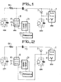
- Figure 1 very schematically shows the conventional arrangement of a microwave transmitter of the cathode modulation type.
- the emission tube 1 is an EIO tube comprising a cathode 2, an anode 3 and a collector 4 connected to ground.
- the modulation switch is a tube 8 with a cathode 9; a grid 10 supplied from a premodulator 22 through a pulse transformer 21 and an anode 11 connected to a second power source 12 with a filtering capacity 13 at its terminals.
- a resistor 14 and a reservoir capacity 15 are disposed in the link connecting the switch 8 to the emitter tube 1.
- the values of the voltages of the sources 5 and 12 are very different and depend on the microwave tube used. As an example, consider a tube in which these voltages vary from simple to double, the value of the voltage of the source 5 being of the order of + 8 KV and that of the source 12 of the order of + 16 KV.
- the cathode 2 of the emitter tube 1 which was brought to the same potential as the anode, must be brought to a new potential value, negative with respect to this electrode.
- This value is -16KV compared to the anode 3 and therefore -24KV compared to the collector 4.
- the latter conducts and transmits a negative front of 16KV on the the anode of diode 7, bringing the potential of cathode 2 of tube 1 to -16KV relative to its anode 3 and therefore to -24KV relative to its collector 4.
- the source 5 in this case provides the potential difference between the anode 3 and the collector 4 necessary for the emitter tube 1 while the second source 12 voltage must provide a voltage value equal to the potential difference required between the anode 3 and the cathode 2 of the tube at the time of emission.
- the object of the invention is to define an arrangement which makes it possible to reduce these drawbacks, that is to say to work with lower voltage values resulting in a reduction in the volume of the components and increasing the reliability of the equipment.
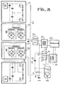
- FIGS. 2 and 3 showing in a way schematic the assembly of the transmitter of the modulation type by its cathode according to the invention and FIG. 3 representing a more detailed diagram of the modulation switch according to the invention.
- FIG. 2 schematically represents the mounting of the emission tube, modulated by the cathode, according to the invention.
- the diagram of FIG. 2 using the same components as that of FIG. 1, the references of the elements common to the two diagrams are the same.
- the mounting of the switch of FIG. 2 is however different from that of FIG. 1. While according to the prior art, the cathode 9 of the switch tube 8 was connected to ground, according to the invention, this cathode is connected directly to the anode 3 of the emitter tube 1.
- the operation of the device is as follows.
- the tank capacity 15 is always loaded at potential, the sum of the absolute values of the voltages supplied by two sources 5 and 12 connected in series.
- the value of the voltage of the source 12 is lower in the assembly according to the invention than in the assembly according to the prior art. This value is reduced, reaching in the example considered half of the value it had, ie 8 KV.
- the tank capacity 15 is then only charged at 16KV. This decrease in the voltage supplied by one of the sources follows of the mounting characteristic according to the invention. Indeed, during the emission, that is to say when the tube 1 is triggered, the voltage of the reservoir capacity is no longer applied between the cathode 2 and the collector 4 of the tube 1, but simply between the cathode 2 and the anode 3. It is then noted that the anode 3 of the tube 1 is permanently brought to the voltage of the power source 5, ie -8KV, relative to the collector 4.
- the cathode 2 of said tube must have a potential equal to -16KV relative to its anode and a potential equal to -24KV relative to its collector C.
- the source 12 has more to provide than a potential difference value equal to the difference between the anode-cathode voltage of the emitter tube and the anode-collector voltage of this same tube. It is obvious under these conditions that the nominal voltage of the source 12 may be much lower than the value which it must have in the assembly according to the prior art. We have seen in the previous explanations that this voltage went from the value 16 KV to the value 8 KV.
- the source 12 would only have to supply a voltage value of 2 KV , instead of 12 KV.
- the mounting of the modulation switch 8 carried out according to the invention makes it possible to reduce the total value of the supply voltages required.
- the power source 5 having to keep its nominal value, the source 12 contributing to the charge of the tank capacity 15, can be of a value much lower than that which it presents in the assembly of the prior art.
- FIG. 3 represents a more detailed diagram of the modulation switch according to the invention in which the power supplies have been shown. These are identified by the references 16 and 17. These are switching power supplies which charge the filtering capacities 6 and 13, via the high voltage transformers, 18 and 19.
- the triode lamp 20 advantageously replaces the resistor 14 of the diagram of Figure 2; it is put to the "cut-off" during the emission and, leading from the end of the emission quickly discharges the parasitic capacity between the cathode 2 and the anode 3 of the modulator tube.
- the grid of this triode is supplied from of the premodulator 22 through a pulse transformer 23.
- a microwave transmitter of the cathode modulation type has thus been described.
Landscapes
- Microwave Tubes (AREA)
- Amplifiers (AREA)
Applications Claiming Priority (2)
| Application Number | Priority Date | Filing Date | Title |
|---|---|---|---|
| FR8214437 | 1982-08-20 | ||
| FR8214437A FR2532057A1 (fr) | 1982-08-20 | 1982-08-20 | Dispositif modulateur pour tube hyperfrequence |
Publications (3)
| Publication Number | Publication Date |
|---|---|
| EP0102290A2 true EP0102290A2 (de) | 1984-03-07 |
| EP0102290A3 EP0102290A3 (en) | 1984-04-04 |
| EP0102290B1 EP0102290B1 (de) | 1986-08-06 |
Family
ID=9276990
Family Applications (1)
| Application Number | Title | Priority Date | Filing Date |
|---|---|---|---|
| EP83401652A Expired EP0102290B1 (de) | 1982-08-20 | 1983-08-11 | Modulationseinrichtung für eine Hochfrequenzröhre |
Country Status (3)
| Country | Link |
|---|---|
| EP (1) | EP0102290B1 (de) |
| DE (1) | DE3365138D1 (de) |
| FR (1) | FR2532057A1 (de) |
Family Cites Families (3)
| Publication number | Priority date | Publication date | Assignee | Title |
|---|---|---|---|---|
| US3339146A (en) * | 1964-07-29 | 1967-08-29 | Alexander A Gorski | Fast rise and fall time rf burst amplifier |
| US3414825A (en) * | 1966-08-18 | 1968-12-03 | Army Usa | Discharge device controlled by on circuit and off circuit with excessive current-limiting means in off circuit |
| US3806836A (en) * | 1972-01-10 | 1974-04-23 | R Alsmeyer | Simplified floating deck pulse modulator |
-
1982
- 1982-08-20 FR FR8214437A patent/FR2532057A1/fr active Granted
-
1983
- 1983-08-11 EP EP83401652A patent/EP0102290B1/de not_active Expired
- 1983-08-11 DE DE8383401652T patent/DE3365138D1/de not_active Expired
Also Published As
| Publication number | Publication date |
|---|---|
| DE3365138D1 (en) | 1986-09-11 |
| FR2532057A1 (fr) | 1984-02-24 |
| FR2532057B1 (de) | 1985-02-08 |
| EP0102290B1 (de) | 1986-08-06 |
| EP0102290A3 (en) | 1984-04-04 |
Similar Documents
| Publication | Publication Date | Title |
|---|---|---|
| US3694659A (en) | Automatic control circuit for image intensifier | |
| CH646283A5 (fr) | Dispositif onduleur convertisseur continu-alternatif a valves commandees. | |
| FR2477338A1 (fr) | Circuit de sortie empeche de se bloquer du fait d'impulsions de tension produites par une charge inductive | |
| FR2610149A1 (fr) | Convertisseur continu-continu a rendement eleve a faible charge | |
| FR2516731A1 (fr) | Circuit servant a convertir une tension continue d'entree en une tension continue de sortie | |
| FR2558304A1 (fr) | Lampe a incandescence a circuit de ballast ameliore | |
| FR2474215A1 (fr) | Alimentation commutee pour tube a rayons cathodiques a couleur variant avec l'energie de penetration | |
| FR2763765A1 (fr) | Commutateur de courant et boucle a phase asservie utilisant ce commutateur | |
| EP0102290B1 (de) | Modulationseinrichtung für eine Hochfrequenzröhre | |
| EP3345456A1 (de) | Elektronischer wandler und beleuchtungssystem mit solch einem wandler | |
| EP0430765B1 (de) | Impuls-Stromversorgungssystem für eine Last, mit Mitteln um die durch die Last möglicherweise reflektierte Energie abzuleiten | |
| US5046152A (en) | Ignition circuit for a gas discharge lamp | |
| WO1993003537A1 (fr) | Convertisseur statique d'energie electrique a semi-conducteurs | |
| EP0645886B1 (de) | Hochenergiezündgenerator insbesondere für eine Gasturbine | |
| EP0147306A2 (de) | Linearer Leistungsverstärker | |
| FR2493651A1 (fr) | Circuit prevu dans un dispositif de reproduction d'images et servant a convertir une tension continue d'entree en une tension continue de sortie | |
| US3601653A (en) | Gas laser with automatic ignition | |
| CA1173106A (fr) | Onduleur a transistors ou a thyristors a recuperation d'energie | |
| EP0681415B1 (de) | Vorrichtung zum Betreiben einer Entladungslampe, insbesondere für die Innenbeleuchtung oder Signalisierung eines Fahrzeuges | |
| SU1619388A1 (ru) | Генератор видеоимпульсов малой длительности | |
| FR2779288A1 (fr) | Module d'alimentation d'une lampe a decharge, notamment de projecteur de vehicule automobile | |
| BE528665A (de) | ||
| EP0414840A1 (de) | Beleuchtungsanordnung mit gasröhren | |
| EP0540375A1 (de) | Zündungsgenerator mit einer hohen Energie, insbesondere für Gasturbinen | |
| US2124719A (en) | Electric wave generator |
Legal Events
| Date | Code | Title | Description |
|---|---|---|---|
| PUAI | Public reference made under article 153(3) epc to a published international application that has entered the european phase |
Free format text: ORIGINAL CODE: 0009012 |
|
| PUAL | Search report despatched |
Free format text: ORIGINAL CODE: 0009013 |
|
| AK | Designated contracting states |
Designated state(s): BE DE FR GB IT NL |
|
| AK | Designated contracting states |
Designated state(s): BE DE FR GB IT NL |
|
| 17P | Request for examination filed |
Effective date: 19840622 |
|
| GRAA | (expected) grant |
Free format text: ORIGINAL CODE: 0009210 |
|
| AK | Designated contracting states |
Kind code of ref document: B1 Designated state(s): BE DE FR GB IT NL |
|
| ITF | It: translation for a ep patent filed | ||
| REF | Corresponds to: |
Ref document number: 3365138 Country of ref document: DE Date of ref document: 19860911 |
|
| PLBE | No opposition filed within time limit |
Free format text: ORIGINAL CODE: 0009261 |
|
| STAA | Information on the status of an ep patent application or granted ep patent |
Free format text: STATUS: NO OPPOSITION FILED WITHIN TIME LIMIT |
|
| 26N | No opposition filed | ||
| PGFP | Annual fee paid to national office [announced via postgrant information from national office to epo] |
Ref country code: DE Payment date: 19890714 Year of fee payment: 7 |
|
| PGFP | Annual fee paid to national office [announced via postgrant information from national office to epo] |
Ref country code: GB Payment date: 19890731 Year of fee payment: 7 |
|
| PGFP | Annual fee paid to national office [announced via postgrant information from national office to epo] |
Ref country code: FR Payment date: 19890822 Year of fee payment: 7 |
|
| ITTA | It: last paid annual fee | ||
| PG25 | Lapsed in a contracting state [announced via postgrant information from national office to epo] |
Ref country code: BE Effective date: 19890831 |
|
| PGFP | Annual fee paid to national office [announced via postgrant information from national office to epo] |
Ref country code: NL Payment date: 19890831 Year of fee payment: 7 |
|
| BERE | Be: lapsed |
Owner name: THOMSON-CSF Effective date: 19890831 |
|
| PG25 | Lapsed in a contracting state [announced via postgrant information from national office to epo] |
Ref country code: GB Effective date: 19900811 |
|
| PG25 | Lapsed in a contracting state [announced via postgrant information from national office to epo] |
Ref country code: NL Effective date: 19910301 |
|
| GBPC | Gb: european patent ceased through non-payment of renewal fee | ||
| NLV4 | Nl: lapsed or anulled due to non-payment of the annual fee | ||
| PG25 | Lapsed in a contracting state [announced via postgrant information from national office to epo] |
Ref country code: FR Effective date: 19910430 |
|
| PG25 | Lapsed in a contracting state [announced via postgrant information from national office to epo] |
Ref country code: DE Effective date: 19910501 |
|
| REG | Reference to a national code |
Ref country code: FR Ref legal event code: ST |