EP0102183B1 - Improvements relating to the starting of discharge lamps - Google Patents
Improvements relating to the starting of discharge lamps Download PDFInfo
- Publication number
- EP0102183B1 EP0102183B1 EP83304251A EP83304251A EP0102183B1 EP 0102183 B1 EP0102183 B1 EP 0102183B1 EP 83304251 A EP83304251 A EP 83304251A EP 83304251 A EP83304251 A EP 83304251A EP 0102183 B1 EP0102183 B1 EP 0102183B1
- Authority
- EP
- European Patent Office
- Prior art keywords
- voltage
- lamp
- circuit
- switch
- pulse
- Prior art date
- Legal status (The legal status is an assumption and is not a legal conclusion. Google has not performed a legal analysis and makes no representation as to the accuracy of the status listed.)
- Expired
Links
Images


Classifications
-
- H—ELECTRICITY
- H05—ELECTRIC TECHNIQUES NOT OTHERWISE PROVIDED FOR
- H05B—ELECTRIC HEATING; ELECTRIC LIGHT SOURCES NOT OTHERWISE PROVIDED FOR; CIRCUIT ARRANGEMENTS FOR ELECTRIC LIGHT SOURCES, IN GENERAL
- H05B41/00—Circuit arrangements or apparatus for igniting or operating discharge lamps
- H05B41/02—Details
- H05B41/04—Starting switches
- H05B41/042—Starting switches using semiconductor devices
- H05B41/044—Starting switches using semiconductor devices for lamp provided with pre-heating electrodes
- H05B41/046—Starting switches using semiconductor devices for lamp provided with pre-heating electrodes using controlled semiconductor devices
Definitions
- This invention relates to the starting of discharge lamps by electronic starter circuits, in particular such circuits employing the pulse producing properties of a non-linear dielectric element, which will be referred to hereinafter as a voltage dependent capacitor or VDC.
- Patent Application No. 2 035 287A also illustrates a circuit utilising a voltage dependent capacitor to provide an ignition pulse for a discharge lamp. This utilises the fact that as the saturation voltage is exceeded the capacitance falls rapidly and current through the element falls sharply to zero. If the capacitor is connected in series with a lamp ballast inductance, the sudden saturation of the capacitor can give rise to a high for ignition of the lamp.
- circuits of the said Patent Application suffers from certain defects for some purposes. Further circuits employing a voltage dependent capacitor are disclosed in European Patent Application publication No. 0-048 137 AI, which is more particularly directed to circuits for lamp ignition. In addition to disclosing several circuits stated to be conventional, the said European Patent Application discloses circuits, starting at Figure 8, in which a voltage dependent capacitor is connected in parallel with a semiconductor switch and in series with a second semiconductor switch. One of these switches serves to control the flow of preheating current to the lamp electrodes and the other to provide a path for the current through the VDC when it suddenly reduces to generate the large ignition pulses required.
- a discharge lamp starter circuit having two starter input terminals for connecting to the cathodes (2, 3) of a discharge lamp (1) to receive a cyclically varying voltage supplied through both the lamp cathodes and a choke ballast (5), the starter circuit including a semiconductor switch (S), triggerable in response to a voltage thereacross, a voltage dependent capacitor (C v ) capable of providing a voltage pulse substantially in excess of twice the peak of said cyclically varying voltage in response to a voltage pulse higher than the saturation voltage thereof, the starter circuit being characterised by provision of a circuit (D1, D2, D3) arranged to cooperate with the switch to connect the switch for conduction in one direction with respect to the input terminals, in one part of a starting cycle, to pass preheating current through the lamp cathodes, and, in another part of said starting cycle, to connect the switch for conduction in the opposite direction with respect to the input terminals and in series with the voltage dependent capacitor (C v ), thereby for conducting a falling current pulse produced by
- the circuit arranged to cooperate with said switch may be a diode steering circuit.
- Circuit elements may be introduced into the path including the voltage dependent capacitor to vary its operation.
- Such elements include means to prevent the voltage dependent capacitor charging until a predetermined voltage has been reached or means for damping a pulse of one polarity resulting from saturation.
- the semiconductor switch may be a self triggering breakback device, otherwise a trigger circuit will be included.
- a circuit may be provided to make the trigger circuit responsive to the cyclically varying voltage selectively in preference to short duration voltage pulses thereby being suitable for starting lamps exhibiting high re-ignition voltages, for example T8 Krypton filled lamps.
- the circuits are preferably arranged to reduce or prevent stressing of the voltage dependent capacitor when the lamp is running.
- the starter includes a circuit requiring a progressively increasing trigger voltage and thereby providing progressively decreasing preheat current pulses.
- the circuit may be arranged to provide ignition pulses of progressively increasing magnitude, at least after a predetermined portion of a starting period and up to the end of a second predetermined portion.
- the present invention provides starter circuits which are believed to be more efficient than prior art circuits and advantageous at least by providing the capability of provision of more advanced features.
- the circuit of the invention uses the realisation that in prior art circuits, in which the disadvantages due to flow of charging and discharging currents through a voltage dependent capacitor have been recognised, for example European Patent Application 0 048 137, page 11, the solution has involved the provision of two semiconductor switches with consequent increase in complexity and expense. The two switches are performing different functions but at different stages in the operation of the circuit.
- the circuit is shown in a simplified form in Figure 3 in which it is associated with a fluorescent lamp 1, which may be a T12 lamp, of the hot cathode type having two cathodes 2 and 3.
- a fluorescent lamp 1 which may be a T12 lamp
- One side 2a of cathode 2 is connected to one terminal 4 of a mains supply through an inductor or choke ballast 5 and one side, 3a, of the other cathode is connected directly to the other terminal 6 of the mains supply.
- the starter circuit is connected across the other terminals 2b and 3b of the cathodes.
- the circuit comprises a series connection of a diode D 1 and a voltage dependent capacitor C v , in parallel with two diodes D 2 and D 3 in series opposition.
- switch S Connected between the junction of the diode D 1 and C v and the junction between the two diodes D 2 and D 3 is a unidirectional switch S having in parallel therewith a trigger circuit 7.
- switch S will be a semiconductor switch and circuit 7, which will be described in more detail with reference to later Figures, is for operation of the switch.
- the invention does, however, also embrace the use of a self-triggering break back device for which a trigger circuit is not required.
- the diodes D 1 to D 3 comprise a diode steering arrangement which allows the switch S to provide the functions in relation to capacitor C v and the lamp 1, performed in prior art circuits by two different switches.
- switch S There are two principal modes for triggering of switch S. The first is for it to be triggered on before V cv reaches V cs (the saturation voltage). The second, which applies to a circuit such as Figure 3 in which there are no elements in series with capacitor C v' is that V cv reaches V cs before S has triggered whereupon its impedance rises and V cv is the cause of S being triggered on.
- the circuit allows scope for introducing elements in the C v path to vary the operation.
- means can be used to prevent C v charging until a predetermined voltage has been reached, for example by a Zener diode.
- an element such as a resistor may be used to influence the charging of C v and hence the degree of saturation achieved at a given applied voltage.
- the inclusion of such a resistor may also reduce the choke di/dt and hence the magnitude of any positive pulse resulting from the saturation voltage being reached. This may be associated with a diode poled to shunt it when an ignition pulse is provided.
- the magnitude of the voltage across the switch rises towards a theoretical maximum (depending on the 'Q' factor) of peak mains voltage, the ascending pulse being characteristic of the ringing of the choke inductance (L) with stray circuit capacitance (C s ) in the system.
- the voltage across the lamp falls from zero towards minus twice peak mains voltage (again depending on 'Q') and D 1 and D 2 are biassed off.
- the switch S has been arranged to perform the two functions of passing the preheat current for one polarity and passing the ignition pulse with the opposite polarity at the lamp but current flow being in the same direction at the switch and trigger circuit.
- V cv will invariably reach +V cs before the switch trigger voltage is reached.
- the resulting positive pulse will cause the switch S to be triggered whereupon the pulse is immediately truncated via D1.
- This voltage is then superimposed on the next negative half cycle lamp voltage presented to the trigger circuit resulting in a cumulative voltage approaching twice the lamp peak (for example, for a 4ft, 40W, T12 lamp, about 400V). If, as is typical for the same lamp, the fixed trigger voltage of the trigger circuit is set to 300V, the switch S will close, -V cs will be exceeded and a negative pulse produced, the pulse being similarly attenuated by the lamp as before.
- FIG 4 shows one practical embodiment of the circuit of Figure 3 employing a fixed voltage trigger but including means for overcoming the voltage-doubling problem just described.
- the unidirectional switch S is a silicon control rectifier TH1.
- the fixed voltage trigger network comprises a zener diode ZD1 and a resistor R 2 in conventional manner and TH1 is shunted by a resistor R 3 .
- TH1 is shunted by a resistor R 3 .
- diode D 4 and a resistor R 1 in parallel with each other.
- the resistor R 1 is however of sufficient value to aiiow V cv to be carried above +V cs without producing a significant positive pulse as indicated hereinbefore to be an option.
- R 1 has a damping effect on any C v current attenuation thus reducing the resulting pulse.
- D 4 provides a low impedance path across R 1 to enable a larger pulse to be passed.
- the negative ringing pulse, in the ballast and stray capacitances, is presented to the trigger network via D 4 and D 3 , causing ZD1 to triggerTH1 into conduction.
- C v charges to the negative pulse height and is then discharged via D 1 and R 1 as the pulse falls and the ringing current reverses.
- the circuit of Figure 3 in its practical form as shown in Figure 4 is suitable for starting many discharge (fluorescent) lamps, in particular the well known T12 argon filled lamp.
- fluorescent lamp now enjoying increasing use is the T8 Krypton filled lamp which has a higher ignition voltage than earlier lamps.
- the circuit of Figure 4 is not suitable for starting lamps such as T8 Krypton filled lamps having high reignition voltages.
- the circuit of Figure 4 provides a solution to the voltage doubling problem in fixed voltage trigger circuits as described hereinbefore.
- the relatively low fixed trigger voltage renders the circuit unsuitable for lamps having reignition voltages approaching 300V on 240V RMS supplies (or 275V on 220V supplies). With such lamps, not only would the VDC C v be stressed but cathode heating would continue to flow due to triggering of the switch S on positive half cycles of the lamp running waveform.
- An alternative trigger circuit must therefore be considered.
- Figure 5 shows a further development of the circuit of this invention which overcomes this problem and is therefore suitable for T8 Krypton filled lamps.
- the trigger network of Figure 4 is replaced with the network of Diac D s , resistor R 2 and capacitor C, and resistors R 3 and R 4 .
- This is in fact a known type of RC delayed thyristor switch circuit which in this arrangement discriminates against the short duration large re- ignition pulses.
- Resistors R 3 and R 4 serve in place of R 3 in Figure 4 to discharge C v .
- the use of a diac trigger requires some means for suppressing positive pulses to protect the switching device and resistor R, is included for that purpose.
- Figure 6 represents a further development which is preferred to that of Figure 5 since it includes a progressive trigger switch of the type described and claimed in British Patent No. 1 602 456 which provides a progressively increasing trigger voltage and discontinuation of triggering if the lamp does not start, as described in that Patent. This feature ensures that the VDC is not continually stressed if the lamp does not start.
- Figure 7a shows the envelope of the lamp voltage waveform when attempting to start a lamp using the progressive trigger of British Patent No. 1 602 456 and in fact corresponds substantially to Figure 5a of that patent. It will be seen that the positive envelope is rising past the point at which the lamp would normally strike, to a maximum at the point at which the switch ceases to trigger, this rise corresponds to the rise in the trigger voltage as the charge on capacitor C1 ( Figure 6) increases up to ignition.
- the negative voltage envelope which is the envelope of the ignition pulses themselves, is of constant amplitude until ignition occurs or until the switch ceases to trigger.
- this invention allows a progression of the amplitude of the ignition pulses themselves. This is achieved by an appropriate selection of the value of R 1 . It has been noted in relation to Figures 4 and 5 that R 1 controls the charging of C v during starting (and also reduces stressing in the run mode). In the arrangement of Figure 6, R, can be selected to control C v charging so that the ratio of C VH to C VL is gradually increased. Thus if the positive trigger level at the cathode of D 1 progressively increases, the positive voltage across C v over R 1 also progressively increases, fr example from below +V cs to above +V cs . As C v is carried progressively towards and into positive saturation the C v negative pulse amplitude progressively increases due to the hysteresis effect.
- R1 The value of R1 must be low enough to ensure that ignition pulses of sufficient magnitude are ultimately produced and high enough to
- the envelope of Fig. 7c is also preferable in respect of lamp life by reducing cathode damage and the resulting "end blackening" associated with lamp ionization before the cathodes have reached emission temperature.
- a preferred circuit for production purposes is therefore that shown in Figure 8.
- the lamp circuit and lamp voltage waveforms for this circuit are shown in Figure 9 and in that Figure the leading edge of the negative ignition pulse is characterised by the ringing of the ballast choke and the VDC in its low capacitance state (the VDC is connected across the lamp via TH1).
- a first part of a voltage rise (determined by the breakdown voltage of a zener diode ZD2, typically 200V) of the trailing edge is, however, characteristic of ballast/stray capacitance ringing after which the VDC begins to discharge, remaining clamped at 200V below the voltage across the starter and once more influencing the pulse shape.
- C v is biassed fully to +V cs and therefore the maximum change of capacitance is achieved to produce the maximum negative going ignition pulses.
- R 1 is a comparatively low resistance value. Therefore in the region C-D the negative ignition pulse amplitude is constant at its maximum value. As shown in Figure 9, at D if the lamp has not started, as it would usually have done as shown by the inset, then the circuit ceases to operate.
- the voltage dependent capacitor C v also produces positive pulses at fixed times (when +V cs is reached) and consequently the preheat pulses are then initiated at the same conduction angle and cease to progress.
- the voltage dependent capacitor C v After termination of the starting period the voltage dependent capacitor C v is gain forward biassed via diode D 1 and consequently it pulses.
- the pulse then obtained is not limited by conduction ofTH1 and may reach damaging amplitudes.
- a zener diode ZD4 is added. This acts in conjunction with ZD3 to limit the magnitude of pulses from C v .
- the trigger voltage has risen to VR 4 (defined by R 4 C 2 time constant) +V C1 +V ZD1 whereupon any subsequent voltage presented to the trigger circuit will by bypassed via ZD3. If this voltage is sufficiently high (for example if C v pulses), the voltage across R4 will rise and ultimately be clamped by ZD4 thereby protecting TH1.
- the voltage on C v is not limited to V ZD3 .
- the voltage on C v reaches a peak defined by This voltage subsequently discharges towards peak mains voltage (V ZD3 ) through R" ZD2, D s , R 4 , ZD3, D3 and the choke on the next negative half cycle although the actual voltage attained depends essentially on the time constant C v R 4 .
- R 4 The value of R 4 is such that -V cs is not to be exceeded and on the subsequent positive half cycle, no pulse is produced and C v charges to a voltage of + peak mains voltage (V ZD2 ).
- Full pulse production is arranged to be delayed (by the choise of ZD2) until the trigger voltage has progressed above the lamp running voltage.
- the lamp will invariably start on a negative ignition pulse and the subsequent positive voltage applied to the starter (that is the lamp running voltage), whilst remaining below the trigger voltage, will still allow +V cs to be exceeded.
- the consequent pulse is, however, attenuated by the lamp and TH1 is not triggered, the VDC thereby remaining charged to the peak lamp running voltage minus V ZD2 .
- ZD3 and ZD4 perform no function if the lamp strikes before the end of the available starting period.
- D 4 and R 6 may be omitted but in that case the value of R 1 should be closer to that given above for R s .
- references to positive and negative voltages are with respect to neutral mains so that all of the circuits described so far produce negative pulses. It is, however, believed that for circuits of this type superior lamp starting is obtained from positive ignition pulses for reasons which are not entirely understood.
- FIG 10 shows a circuit which is in all essential respects the same as that of Figure 8, and is suitable for starting T8 Krypton filled lamps, but produces positive ignition pulses.
- PFC power factor correction
Abstract
Description
- This invention relates to the starting of discharge lamps by electronic starter circuits, in particular such circuits employing the pulse producing properties of a non-linear dielectric element, which will be referred to hereinafter as a voltage dependent capacitor or VDC.
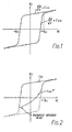
- The chemical composition of a voltage dependent capacitor is described in British Patent Application No. 2 035 287A. An element of that type exhibits a capacitance/voltage characteristic as shown in Figure 1 in which the charge Qc is plotted as a function of the voltage Vc. This characteristic may readily be obtained by the use of an oscilloscope. The incremental capacitance C of the element is the incremental slope so that Cv=6Qc/6Vc. As can readily be seen from Figure 1, on a positive increasing bias there is a high capacitance CvH, which at a voltage Vcs, which may be called the saturation voltage, changes to a low capacitance CVL. Additionally there is an hysteresis effect whereby reverse bias is required before the capacitance can revert to CvH. If, then, a reduced reverse bias is imposed, perhaps by the insertion of a breakdown device, the full value of CVH will not be restored so that a reduced value will be obtained as shown at CVH * in Figure 2. A similar effect is obtained for a first cycle of voltage, rising to positive maximum from zero and not from a negative value.
- Patent Application No. 2 035 287A also illustrates a circuit utilising a voltage dependent capacitor to provide an ignition pulse for a discharge lamp. This utilises the fact that as the saturation voltage is exceeded the capacitance falls rapidly and current through the element falls sharply to zero. If the capacitor is connected in series with a lamp ballast inductance, the sudden saturation of the capacitor can give rise to a high

- The circuit of the said Patent Application suffers from certain defects for some purposes. Further circuits employing a voltage dependent capacitor are disclosed in European Patent Application publication No. 0-048 137 AI, which is more particularly directed to circuits for lamp ignition. In addition to disclosing several circuits stated to be conventional, the said European Patent Application discloses circuits, starting at Figure 8, in which a voltage dependent capacitor is connected in parallel with a semiconductor switch and in series with a second semiconductor switch. One of these switches serves to control the flow of preheating current to the lamp electrodes and the other to provide a path for the current through the VDC when it suddenly reduces to generate the large ignition pulses required.
- It is believed that these circuits also suffer from disadvantages and it is accordingly an object of this invention to provide an improved electronic starter, using a voltage dependent capacitor.
- According to the invention there is provided a discharge lamp starter circuit having two starter input terminals for connecting to the cathodes (2, 3) of a discharge lamp (1) to receive a cyclically varying voltage supplied through both the lamp cathodes and a choke ballast (5), the starter circuit including a semiconductor switch (S), triggerable in response to a voltage thereacross, a voltage dependent capacitor (Cv) capable of providing a voltage pulse substantially in excess of twice the peak of said cyclically varying voltage in response to a voltage pulse higher than the saturation voltage thereof, the starter circuit being characterised by provision of a circuit (D1, D2, D3) arranged to cooperate with the switch to connect the switch for conduction in one direction with respect to the input terminals, in one part of a starting cycle, to pass preheating current through the lamp cathodes, and, in another part of said starting cycle, to connect the switch for conduction in the opposite direction with respect to the input terminals and in series with the voltage dependent capacitor (Cv), thereby for conducting a falling current pulse produced by the voltage dependent capacitor to provide an ignition voltage pulse across the lamp (1).
- The circuit arranged to cooperate with said switch may be a diode steering circuit.
- Circuit elements may be introduced into the path including the voltage dependent capacitor to vary its operation.
- Such elements include means to prevent the voltage dependent capacitor charging until a predetermined voltage has been reached or means for damping a pulse of one polarity resulting from saturation.
- The semiconductor switch may be a self triggering breakback device, otherwise a trigger circuit will be included.
- A circuit may be provided to make the trigger circuit responsive to the cyclically varying voltage selectively in preference to short duration voltage pulses thereby being suitable for starting lamps exhibiting high re-ignition voltages, for example T8 Krypton filled lamps.
- The circuits are preferably arranged to reduce or prevent stressing of the voltage dependent capacitor when the lamp is running.
- Preferably the starter includes a circuit requiring a progressively increasing trigger voltage and thereby providing progressively decreasing preheat current pulses. The circuit may be arranged to provide ignition pulses of progressively increasing magnitude, at least after a predetermined portion of a starting period and up to the end of a second predetermined portion.
- In order that the invention may be clearly understood and readily carried into effect it will now be described by way of example with reference to the accompanying drawings of which:
- Figure 1 shows the charge v. voltage characteristic of a voltage dependent capacitor as described hereinbefore,
- Figure 2 shows the effect on the characteristic of Figure 1 of reducing the negative bias applied thereto as described hereinbefore,
- Figure 3 shows the basic circuit of the present invention,
- Figure 4 shows a practical form of the circuit of Figure 3,
- Figure 5 shows an improved circuit capable of satisfactorily starting lamps with high-reignition voltages,
- Figure 6 shows a circuit incorporating a progressive trigger,
- Figures 7a, 7b and 7c show the effect of the value of resistor R1 in Figure 6 on the lamp starting voltage envelope,
- Figure 8 shows a version of the circuit of Figure 6 more suitable for production purposes,
- Figure 9 shows current and voltage waveforms for the circuit of Figure 8, and
- Figure 10 shows a version of the circuit of Figure 8 arranged to provide positive ignition pulses.
- The present invention provides starter circuits which are believed to be more efficient than prior art circuits and advantageous at least by providing the capability of provision of more advanced features. In its simplest form the circuit of the invention uses the realisation that in prior art circuits, in which the disadvantages due to flow of charging and discharging currents through a voltage dependent capacitor have been recognised, for example European Patent Application 0 048 137, page 11, the solution has involved the provision of two semiconductor switches with consequent increase in complexity and expense. The two switches are performing different functions but at different stages in the operation of the circuit. On that basis we have now devised an arrangement using diode steering in conjunction with a suitable relationship between a single semiconductor switch and the voltage dependent capacitor, to achieve the desired result.
- The circuit is shown in a simplified form in Figure 3 in which it is associated with a fluorescent lamp 1, which may be a T12 lamp, of the hot cathode type having two
cathodes cathode 2 is connected to one terminal 4 of a mains supply through an inductor orchoke ballast 5 and one side, 3a, of the other cathode is connected directly to theother terminal 6 of the mains supply. The starter circuit is connected across the other terminals 2b and 3b of the cathodes. The circuit comprises a series connection of a diode D1 and a voltage dependent capacitor Cv, in parallel with two diodes D2 and D3 in series opposition. Connected between the junction of the diode D1 and Cv and the junction between the two diodes D2 and D3 is a unidirectional switch S having in parallel therewith a trigger circuit 7. It will be appreciated that in any practical circuit, switch S will be a semiconductor switch and circuit 7, which will be described in more detail with reference to later Figures, is for operation of the switch. The invention does, however, also embrace the use of a self-triggering break back device for which a trigger circuit is not required. The diodes D1 to D3 comprise a diode steering arrangement which allows the switch S to provide the functions in relation to capacitor Cv and the lamp 1, performed in prior art circuits by two different switches. - Considering the operation of this circuit, when the switch S is off, the voltage Vcv across capacitor Cv is zero and it is charged to some positive level. With the mains voltage rising from zero to Diode D1 is forward biassed to conduct and Cv is the main load on the
choke ballast 5. The lamp voltage Vlamp is rising with the mains and Vcv is similarly rising, the capacitor charging at the same time. Current also flows through the trigger path via D2, but D3 is reverse biassed and is off. - There are two principal modes for triggering of switch S. The first is for it to be triggered on before Vcv reaches Vcs (the saturation voltage). The second, which applies to a circuit such as Figure 3 in which there are no elements in series with capacitor Cv' is that Vcv reaches Vcs before S has triggered whereupon its impedance rises and Vcv is the cause of S being triggered on.
- It should be noted that the circuit allows scope for introducing elements in the Cv path to vary the operation. For example means can be used to prevent Cv charging until a predetermined voltage has been reached, for example by a Zener diode. Or an element such as a resistor may be used to influence the charging of Cv and hence the degree of saturation achieved at a given applied voltage. The inclusion of such a resistor may also reduce the choke di/dt and hence the magnitude of any positive pulse resulting from the saturation voltage being reached. This may be associated with a diode poled to shunt it when an ignition pulse is provided.
- When switch S is triggered on, Cv is discharged via S and D2 to zero. In practice resistance may be included to control the maximum discharge current. Preheat current flows through the
choke 5, D1, S and D2 and, of course, also through the lamp cathodes providing desired preheating thereof. The voltage across the choke is approximately the mains voltage and the heating current iH lags that voltage. The circuit is arranged so that the choke saturates so that the current, although initially sinusoidal, is increased at the peak. When the current iH reduces to approximately zero the switch S commutates and switches off. At this stage, as the switch opens, the magnitude of the voltage across the switch rises towards a theoretical maximum (depending on the 'Q' factor) of peak mains voltage, the ascending pulse being characteristic of the ringing of the choke inductance (L) with stray circuit capacitance (Cs) in the system. Simultaneously the voltage across the lamp falls from zero towards minus twice peak mains voltage (again depending on 'Q') and D1 and D2 are biassed off. - However with the reverse of the voltage across the lamp D3 has been biassed on. The rising voltage across switch S causes the switch to be triggered on again and Cv appears in parallel with the stray capacitances Cs. Vcv goes negative as current transfers from Cs to Cv. Vcv is then carried to the saturation voltage -Vcs. If Cv has only fallen from zero the change in capacitance will be relatively small (cf Figure 2) and a small pulse will occur. However if Cv has been to +Vcs or more and back through zero, the value of Cv will fall sharply and correspondingly sharply reduce the current through the choke. The current fall in the choke and Cv then generates a large negative voltage pulse, very much greater than twice peak mains, which provides an ignition pulse for the lamp. Thereafter the fall in current through the switch causes it to commutate again when Vcv reaches the peak negative pulse voltage. As the lamp voltage rises towards zero, Cv discharges via diode D1 such that Vcv is substantially equal to the voltage across the lamp. When the lamp voltage passes through zero, diode D, continues to be forwarded biassed, Cv charges and the cycle repeats.
- It will be seen from this account that the switch S has been arranged to perform the two functions of passing the preheat current for one polarity and passing the ignition pulse with the opposite polarity at the lamp but current flow being in the same direction at the switch and trigger circuit.
- To prevent re-triggering when the lamp is running a high trigger voltage is necessary. Since the saturation voltage of Cv is typically 50V then, for the basic circuit of Figure 3, Vcv will invariably reach +Vcs before the switch trigger voltage is reached. Thus assuming -Vcs has previously been exceeded, the resulting positive pulse will cause the switch S to be triggered whereupon the pulse is immediately truncated via D1.
- Since there is full positive saturation of Cv a maximum negative ignition pulse will be realised.
- If the ignition pulse starts the lamp the circuit is still required to operate in the running mode in which re-ignition pulses occur on each mains cycle. As has been pointed out in the prior art it is undesirable for the voltage dependent capacitor to be stressed during lamp running.
- With the circuit of Figure 3, the negative lamp running voltage is prevented from charging Cv towards Vcs by the open circuit switch S (if it is insufficient to trigger it). Consequently, since Cv does not in these circumstances become negatively biassed, positive lamp voltages, although exceeding +Vcs, cannot cause stressing in view of the hysteresis effect.
- A critical consideration in the preceding paragraph is that the negative reignition pulses are insufficient to trigger the switch S. This is not satisfied for many lamps by the circuit of Figure 3 when a simple fixed voltage trigger circuit is employed.
- It has been stated hereinbefore that when +Vcs is reached, the switch S triggers (due to positive pulse production) and conduction via diode D1 truncates the resulting pulse. This condition, however, prevails only during the starting cycle. If, for example, the lamp strikes on a given negative ignition pulse then, on the next positive half cycle, +Vcs will be exceeded but the resulting pulse is attenuated by the relatively low impedance of the ionized lamp. Some increase in peak positive lamp voltage may be observed although the trigger circuit would normally be adjusted such that the trigger voltage exceeds this value and thus no positive triggering of switch S would occur.
- This voltage is then superimposed on the next negative half cycle lamp voltage presented to the trigger circuit resulting in a cumulative voltage approaching twice the lamp peak (for example, for a 4ft, 40W, T12 lamp, about 400V). If, as is typical for the same lamp, the fixed trigger voltage of the trigger circuit is set to 300V, the switch S will close, -Vcs will be exceeded and a negative pulse produced, the pulse being similarly attenuated by the lamp as before.
- This voltage-doubling condition will be maintained throughout the period of lamp operation.
- Thus, whilst no cathode heating current will flow (since there is no triggering on positive half cycles), the general circuit of Fig. 3 (assuming a fixed voltage trigger) will not prevent stressing of the VDC where the peak lamp running voltage exceeds 150V.
- (It should be noted that the figure of 150V includes any increase in the normal lamp running voltage due to pulse production when +Vcs is exceeded and neglects the safety margins and circuit tolerances which are normally applied).
- The circuit of Figure 3 with a fixed voltage trigger is therefore unsuitable for lamps other than 2 ft., 20W, T11 and below.
- On 220V supplies, the circuit is even more impractical since a maximum trigger voltage of around 275V would be required to ensure operation at the lowest supply voltage of 198V RMS.
- Figure 4 shows one practical embodiment of the circuit of Figure 3 employing a fixed voltage trigger but including means for overcoming the voltage-doubling problem just described. In this circuit the unidirectional switch S is a silicon control rectifier TH1. The fixed voltage trigger network comprises a zener diode ZD1 and a resistor R2 in conventional manner and TH1 is shunted by a resistor R3. In series with Cv there is a diode D4 and a resistor R1 in parallel with each other. Basically the operation is the same as that described with reference to Figure 3. The resistor R1 is however of sufficient value to aiiow Vcv to be carried above +Vcs without producing a significant positive pulse as indicated hereinbefore to be an option. R1 has a damping effect on any Cv current attenuation thus reducing the resulting pulse. During negative ignition pulse production D4 provides a low impedance path across R1 to enable a larger pulse to be passed. The negative ringing pulse, in the ballast and stray capacitances, is presented to the trigger network via D4 and D3, causing ZD1 to triggerTH1 into conduction. Cv charges to the negative pulse height and is then discharged via D1 and R1 as the pulse falls and the ringing current reverses.
- When the lamp has started, if reignition pulses are less than the breakdown voltage VZ, of ZD1 no switch triggering occurs. As a result of introducing the resistor R, the capacitor Cv is charged to less than the positive peak lamp running voltage. Hence the cumulative voltage applied to the trigger circuit during running is now considerably less than twice the peak lamp running voltage and TH1 does not trigger. Now because only positive reignition pulses are applied to Cv stressing does not occur. Resistor R3 is included across TH1 to ensure that on lamp starting, positive cycle charging of Cv via D, and R, can be discharged via D4, R3 and D2.
- In the description of the starting cycles of Figures 3 and 4 it has been assumed that the switch S commutates, as preheat current returns to zero, and supports the subsequent ringing voltage. For standard thyristors with slower response, TH1 may not commutate and in that case Cv receives the choke current*immediately it reverses through TH1. Thus it is not necessary to retrigger TH1 on again during ignition pulse production.
- The circuit of Figure 3 in its practical form as shown in Figure 4 is suitable for starting many discharge (fluorescent) lamps, in particular the well known T12 argon filled lamp. However a fluorescent lamp now enjoying increasing use is the T8 Krypton filled lamp which has a higher ignition voltage than earlier lamps. In general the circuit of Figure 4 is not suitable for starting lamps such as T8 Krypton filled lamps having high reignition voltages.
- The circuit of Figure 4 provides a solution to the voltage doubling problem in fixed voltage trigger circuits as described hereinbefore. However, even if the effect can be completely eliminated, the relatively low fixed trigger voltage renders the circuit unsuitable for lamps having reignition voltages approaching 300V on 240V RMS supplies (or 275V on 220V supplies). With such lamps, not only would the VDC Cv be stressed but cathode heating would continue to flow due to triggering of the switch S on positive half cycles of the lamp running waveform. An alternative trigger circuit must therefore be considered.
- Figure 5 shows a further development of the circuit of this invention which overcomes this problem and is therefore suitable for T8 Krypton filled lamps. The trigger network of Figure 4 is replaced with the network of Diac Ds, resistor R2 and capacitor C, and resistors R3 and R4. This is in fact a known type of RC delayed thyristor switch circuit which in this arrangement discriminates against the short duration large re- ignition pulses. Resistors R3 and R4 serve in place of R3 in Figure 4 to discharge Cv. The use of a diac trigger, however, requires some means for suppressing positive pulses to protect the switching device and resistor R, is included for that purpose.
- Figure 6 represents a further development which is preferred to that of Figure 5 since it includes a progressive trigger switch of the type described and claimed in British Patent No. 1 602 456 which provides a progressively increasing trigger voltage and discontinuation of triggering if the lamp does not start, as described in that Patent. This feature ensures that the VDC is not continually stressed if the lamp does not start.
- Figure 7a shows the envelope of the lamp voltage waveform when attempting to start a lamp using the progressive trigger of British Patent No. 1 602 456 and in fact corresponds substantially to Figure 5a of that patent. It will be seen that the positive envelope is rising past the point at which the lamp would normally strike, to a maximum at the point at which the switch ceases to trigger, this rise corresponds to the rise in the trigger voltage as the charge on capacitor C1 (Figure 6) increases up to ignition. The negative voltage envelope, which is the envelope of the ignition pulses themselves, is of constant amplitude until ignition occurs or until the switch ceases to trigger.
- It has, however, now been realised that this invention allows a progression of the amplitude of the ignition pulses themselves. This is achieved by an appropriate selection of the value of R1. It has been noted in relation to Figures 4 and 5 that R1 controls the charging of Cv during starting (and also reduces stressing in the run mode). In the arrangement of Figure 6, R, can be selected to control Cv charging so that the ratio of CVH to CVL is gradually increased. Thus if the positive trigger level at the cathode of D1 progressively increases, the positive voltage across Cv over R1 also progressively increases, fr example from below +Vcs to above +Vcs. As Cv is carried progressively towards and into positive saturation the Cv negative pulse amplitude progressively increases due to the hysteresis effect.
- The value of R1 must be low enough to ensure that ignition pulses of sufficient magnitude are ultimately produced and high enough to
- (i) reduce the positive pulse amplitude to within the switching device capability; and
- (ii) reduce the rate of increase of ignition pulses to prevent "cold starting" (i.e. lamp ionization before cathode emission temperature is reached).
- A careful compromise is therefore necessary, but the choice will provide no problem to a practical circuit engineer in view of the values of other circuit elements.
- For low values of R1 the envelope will be the same as that of Patent No. 1 602 456 and as shown in Figure 7a.
- If R1 is increased the envelope will become that of Figure 7b in which the negative pulse amplitude starts low but increases to maximum before ignition.
- Further increasing R1 gives the envelope of Figure 7c which provides the best visual lamp start by delaying the application of the high negative voltage pulse until the progression voltage exceeds the lamp re-ignition voltage. This is advantageous as no lamp ionisation occurs while the lamp cathodes are being heated, and then the rapid progression of high negative voltage pulses ensures a flicker-free start.
- The envelope of Fig. 7c is also preferable in respect of lamp life by reducing cathode damage and the resulting "end blackening" associated with lamp ionization before the cathodes have reached emission temperature.
- The circuit of Figure 6 does suffer from one minor defect in the value of R1 required to produce the preferred progression of Figure 7c is so large that Cv is not fully positively biassed within the starting cycle and maximum negative pulses are not realised.
- A preferred circuit for production purposes is therefore that shown in Figure 8. The lamp circuit and lamp voltage waveforms for this circuit are shown in Figure 9 and in that Figure the leading edge of the negative ignition pulse is characterised by the ringing of the ballast choke and the VDC in its low capacitance state (the VDC is connected across the lamp via TH1).
- Since the VDC has not been positively biassed no high voltage pulse due to capacitance change occurs.
- A first part of a voltage rise (determined by the breakdown voltage of a zener diode ZD2, typically 200V) of the trailing edge is, however, characteristic of ballast/stray capacitance ringing after which the VDC begins to discharge, remaining clamped at 200V below the voltage across the starter and once more influencing the pulse shape.
- In the region B-C the high and increasing positive trigger voltages exceed the breakdown voltage of ZD2 and are allowed to bias Cv progressively more positive, over ZD2 and R1. This gives rise to progressively increasing negative ignition pulses, with a steeply rising envelope, because of the effect of the hysteresis as discussed hereinbefore.
- At C, Cv is biassed fully to +Vcs and therefore the maximum change of capacitance is achieved to produce the maximum negative going ignition pulses. To ensure that maximum pulses can be achieved R1 is a comparatively low resistance value. Therefore in the region C-D the negative ignition pulse amplitude is constant at its maximum value. As shown in Figure 9, at D if the lamp has not started, as it would usually have done as shown by the inset, then the circuit ceases to operate.
- In the region C-D the voltage dependent capacitor Cv also produces positive pulses at fixed times (when +Vcs is reached) and consequently the preheat pulses are then initiated at the same conduction angle and cease to progress.
- Unless the lamp strikes the progressing positive Cv pulses would of themselves keep on triggering the switch TH1 even though the breakdown voltage of ZD1 and the voltage on C1 together exceed peak mains. For this response it would appear that there would be no termination to the starting period until the trigger voltage progresses above the peak positive pulse produced by the action of Cv. A further zener diode ZD3 is therefore included to terminate the starting period with ZD1 determining the initial triggering level. Thus a constant starting period is obtained independent of the mains supply voltage.
- After termination of the starting period the voltage dependent capacitor Cv is gain forward biassed via diode D1 and consequently it pulses. The pulse then obtained is not limited by conduction ofTH1 and may reach damaging amplitudes. To prevent this and to prevent TH1 from having to withstand such pulses a zener diode ZD4 is added. This acts in conjunction with ZD3 to limit the magnitude of pulses from Cv.
- At termination, assuming the lamp has failed to start, the trigger voltage has risen to VR4 (defined by R4C2 time constant) +VC1+VZD1 where

- The voltage on Cv is not limited to VZD3. When the last positive pulse occurs (which is not attenuated by conduction of TH1), the voltage on Cv reaches a peak defined by

- The value of R4 is such that -Vcs is not to be exceeded and on the subsequent positive half cycle, no pulse is produced and Cv charges to a voltage of + peak mains voltage (VZD2).
- This cycle then continues until the supply is removed.
- Full pulse production is arranged to be delayed (by the choise of ZD2) until the trigger voltage has progressed above the lamp running voltage. The lamp will invariably start on a negative ignition pulse and the subsequent positive voltage applied to the starter (that is the lamp running voltage), whilst remaining below the trigger voltage, will still allow +Vcs to be exceeded. The consequent pulse is, however, attenuated by the lamp and TH1 is not triggered, the VDC thereby remaining charged to the peak lamp running voltage minus VZD2.
- This voltage is then superimposed on the following negative half cycle of the lamp running voltage and presented to the trigger circuit. However, the time constant R4Cz prevents TH1 from being triggered, some charge being lost from the VDC through this network.
- Cv is recharged on the next positive half cycle but no pulse is produced since -Vcs has not previously been exceeded. The cycle will then continue throughout the period of lamp operation.
- Thus ZD3 and ZD4 perform no function if the lamp strikes before the end of the available starting period.
- When the lamp is running any positive charging of Cv during re-ignition pulses is prevented from triggering TH1 by the delay C2 and R4. Cv is never negatively biassed, since TH1 is always off, and consequently no positive pulse can be produced and negative re-ignition pulses see a non-conducting TH1.
- For a typical production circuit of the form shown in Figure 8, suitable for starting T8 Krypton filled lamps, the following component values are suitable:


- With these values a typical starting cycle at 240 volts 50 Hz takes one second and a typical peak negative pulse reaches 2000 volts.
- It should be noted that D4 and R6 may be omitted but in that case the value of R1 should be closer to that given above for Rs.
- With respect to all of the description herein, references to positive and negative voltages are with respect to neutral mains so that all of the circuits described so far produce negative pulses. It is, however, believed that for circuits of this type superior lamp starting is obtained from positive ignition pulses for reasons which are not entirely understood.
- For this reason Figure 10 shows a circuit which is in all essential respects the same as that of Figure 8, and is suitable for starting T8 Krypton filled lamps, but produces positive ignition pulses. Apart from the conventional power factor correction (PFC) capacitor the most striking difference is the replacement of diode D2 with three individual diodes. This is, however, a minor matter of circuit design. It will be appreciated in consideration of the operation of this circuit the description, given hereinbefore will apply with appropriate interchange of polarities.
- It will be appreciated that a circuit such as that of Figure 10 takes pre-heating current in one direction from the mains supply during starting. This is clearly undesirable where many such starters are provided in one installation. The problem may be reduced however if a proportion of starters (approaching 50% preferably) take current of the opposite polarity. This may be arranged for circuits such as that of Figure 10 (or Figure 8) by reversing the terminal block connections so that, as shown in Figure 10, the live (L) and neutral (N) terminals are reversed. This has the effect of moving the ballast choke to the neutral lead so that the ignition pulse is still positive (Figure 10) although of reduced magnitude relative to neutral.
- Other implementations of this invention will be apparent to those skilled in lighting circuits.
Claims (10)
Priority Applications (1)
| Application Number | Priority Date | Filing Date | Title |
|---|---|---|---|
| AT83304251T ATE32823T1 (en) | 1982-08-05 | 1983-07-22 | IGNITION OF DISCHARGE LAMPS. |
Applications Claiming Priority (2)
| Application Number | Priority Date | Filing Date | Title |
|---|---|---|---|
| GB8222651 | 1982-08-05 | ||
| GB8222651 | 1982-08-05 |
Publications (3)
| Publication Number | Publication Date |
|---|---|
| EP0102183A2 EP0102183A2 (en) | 1984-03-07 |
| EP0102183A3 EP0102183A3 (en) | 1985-01-23 |
| EP0102183B1 true EP0102183B1 (en) | 1988-03-02 |
Family
ID=10532143
Family Applications (1)
| Application Number | Title | Priority Date | Filing Date |
|---|---|---|---|
| EP83304251A Expired EP0102183B1 (en) | 1982-08-05 | 1983-07-22 | Improvements relating to the starting of discharge lamps |
Country Status (6)
| Country | Link |
|---|---|
| EP (1) | EP0102183B1 (en) |
| AT (1) | ATE32823T1 (en) |
| AU (1) | AU559657B2 (en) |
| DE (1) | DE3375874D1 (en) |
| NZ (1) | NZ205154A (en) |
| ZA (1) | ZA835513B (en) |
Families Citing this family (1)
| Publication number | Priority date | Publication date | Assignee | Title |
|---|---|---|---|---|
| DE3327189A1 (en) * | 1983-07-28 | 1985-02-07 | Diehl GmbH & Co, 8500 Nürnberg | Circuit arrangement for the starting and brightness control of fluorescent lamps |
Family Cites Families (2)
| Publication number | Priority date | Publication date | Assignee | Title |
|---|---|---|---|---|
| DE2949074A1 (en) * | 1979-12-06 | 1981-06-11 | Philips Patentverwaltung Gmbh, 2000 Hamburg | Voltage impulse generator for striking gas discharge lamp - uses specified lead lanthanum titanate zirconate dielectric for nonlinear capacitor |
| JPS5750797A (en) * | 1980-09-11 | 1982-03-25 | Mitsubishi Electric Corp | Device for firing discharge lamp |
-
1983
- 1983-07-22 EP EP83304251A patent/EP0102183B1/en not_active Expired
- 1983-07-22 DE DE8383304251T patent/DE3375874D1/en not_active Expired
- 1983-07-22 AT AT83304251T patent/ATE32823T1/en not_active IP Right Cessation
- 1983-07-28 ZA ZA835513A patent/ZA835513B/en unknown
- 1983-08-02 AU AU17522/83A patent/AU559657B2/en not_active Ceased
- 1983-08-04 NZ NZ205154A patent/NZ205154A/en unknown
Also Published As
| Publication number | Publication date |
|---|---|
| DE3375874D1 (en) | 1988-04-07 |
| ZA835513B (en) | 1984-06-27 |
| EP0102183A2 (en) | 1984-03-07 |
| ATE32823T1 (en) | 1988-03-15 |
| AU559657B2 (en) | 1987-03-19 |
| NZ205154A (en) | 1986-12-05 |
| EP0102183A3 (en) | 1985-01-23 |
| AU1752283A (en) | 1984-02-09 |
Similar Documents
| Publication | Publication Date | Title |
|---|---|---|
| US4937501A (en) | Circuit arrangement for starting a high-pressure gas discharge lamp | |
| EP0333359B1 (en) | Starter circuits for discharge lamps | |
| US4629944A (en) | Starter circuit for a fluorescent tube lamp | |
| US5055742A (en) | Gas discharge lamp dimming system | |
| KR100281373B1 (en) | Electronic ballast for high intensity discharge lamp | |
| US4959593A (en) | Two-lead igniter for HID lamps | |
| US4210850A (en) | Circuits for operating electric discharge lamps | |
| CA1262256A (en) | Dc/ac converter for igniting and feeding a gas and/or vapour discharge lamp | |
| EP0048137B1 (en) | Discharge tube firing circuit | |
| EP0102183B1 (en) | Improvements relating to the starting of discharge lamps | |
| US5572093A (en) | Regulation of hot restrike pulse intensity and repetition | |
| US4539513A (en) | Circuit arrangement for starting and operating a high-pressure gas discharge lamp | |
| US5514938A (en) | D.C. ciruit for starting high pressure discharge lamp | |
| CN1137608C (en) | Circuit arrangement | |
| US4227118A (en) | Circuits for operating electric discharge lamps | |
| US5084655A (en) | Circuit arrangement suitable for igniting a high-pressure discharge lamp | |
| US6153983A (en) | Full wave electronic starter | |
| JPS6251194A (en) | Gas discharge lamp ignition and operation circuit layout | |
| US4816721A (en) | Circuit arrangement for operating a high-pressure gas discharge lamp | |
| US4039895A (en) | Device for starting and feeding a discharge lamp | |
| EP0011410B1 (en) | Electronic starter circuits for discharge lamps | |
| US5781424A (en) | Static converter for an incandescent lamp having a delayed start | |
| US6621237B2 (en) | Gas-discharge lamp lighting apparatus with optimized circuit configuration | |
| EP0034401A2 (en) | Discharge lamp circuit | |
| EP0147922A1 (en) | Ballast circuits for lighting units |
Legal Events
| Date | Code | Title | Description |
|---|---|---|---|
| PUAI | Public reference made under article 153(3) epc to a published international application that has entered the european phase |
Free format text: ORIGINAL CODE: 0009012 |
|
| AK | Designated contracting states |
Designated state(s): AT CH DE FR GB IT LI NL |
|
| PUAL | Search report despatched |
Free format text: ORIGINAL CODE: 0009013 |
|
| AK | Designated contracting states |
Designated state(s): AT CH DE FR GB IT LI NL |
|
| 17P | Request for examination filed |
Effective date: 19850227 |
|
| 17Q | First examination report despatched |
Effective date: 19861009 |
|
| ITF | It: translation for a ep patent filed |
Owner name: FUMERO BREVETTI S.N.C. |
|
| GRAA | (expected) grant |
Free format text: ORIGINAL CODE: 0009210 |
|
| AK | Designated contracting states |
Kind code of ref document: B1 Designated state(s): AT CH DE FR GB IT LI NL |
|
| REF | Corresponds to: |
Ref document number: 32823 Country of ref document: AT Date of ref document: 19880315 Kind code of ref document: T |
|
| REF | Corresponds to: |
Ref document number: 3375874 Country of ref document: DE Date of ref document: 19880407 |
|
| ET | Fr: translation filed | ||
| PLBE | No opposition filed within time limit |
Free format text: ORIGINAL CODE: 0009261 |
|
| STAA | Information on the status of an ep patent application or granted ep patent |
Free format text: STATUS: NO OPPOSITION FILED WITHIN TIME LIMIT |
|
| 26N | No opposition filed | ||
| ITTA | It: last paid annual fee | ||
| PGFP | Annual fee paid to national office [announced via postgrant information from national office to epo] |
Ref country code: GB Payment date: 19920727 Year of fee payment: 10 |
|
| PGFP | Annual fee paid to national office [announced via postgrant information from national office to epo] |
Ref country code: CH Payment date: 19920728 Year of fee payment: 10 |
|
| PGFP | Annual fee paid to national office [announced via postgrant information from national office to epo] |
Ref country code: FR Payment date: 19920730 Year of fee payment: 10 Ref country code: AT Payment date: 19920730 Year of fee payment: 10 |
|
| PGFP | Annual fee paid to national office [announced via postgrant information from national office to epo] |
Ref country code: NL Payment date: 19920731 Year of fee payment: 10 |
|
| PGFP | Annual fee paid to national office [announced via postgrant information from national office to epo] |
Ref country code: DE Payment date: 19920925 Year of fee payment: 10 |
|
| PG25 | Lapsed in a contracting state [announced via postgrant information from national office to epo] |
Ref country code: GB Effective date: 19930722 Ref country code: AT Effective date: 19930722 |
|
| PG25 | Lapsed in a contracting state [announced via postgrant information from national office to epo] |
Ref country code: LI Effective date: 19930731 Ref country code: CH Effective date: 19930731 |
|
| PG25 | Lapsed in a contracting state [announced via postgrant information from national office to epo] |
Ref country code: NL Effective date: 19940201 |
|
| NLV4 | Nl: lapsed or anulled due to non-payment of the annual fee | ||
| GBPC | Gb: european patent ceased through non-payment of renewal fee |
Effective date: 19930722 |
|
| PG25 | Lapsed in a contracting state [announced via postgrant information from national office to epo] |
Ref country code: FR Effective date: 19940331 |
|
| REG | Reference to a national code |
Ref country code: CH Ref legal event code: PL |
|
| PG25 | Lapsed in a contracting state [announced via postgrant information from national office to epo] |
Ref country code: DE Effective date: 19940401 |
|
| REG | Reference to a national code |
Ref country code: FR Ref legal event code: ST |