EP0101344A1 - Information carrier with thermo-destructible magnetic memory elements - Google Patents
Information carrier with thermo-destructible magnetic memory elements Download PDFInfo
- Publication number
- EP0101344A1 EP0101344A1 EP83401444A EP83401444A EP0101344A1 EP 0101344 A1 EP0101344 A1 EP 0101344A1 EP 83401444 A EP83401444 A EP 83401444A EP 83401444 A EP83401444 A EP 83401444A EP 0101344 A1 EP0101344 A1 EP 0101344A1
- Authority
- EP
- European Patent Office
- Prior art keywords
- magnetic
- destructible
- information carrier
- magnetic memory
- memory elements
- Prior art date
- Legal status (The legal status is an assumption and is not a legal conclusion. Google has not performed a legal analysis and makes no representation as to the accuracy of the status listed.)
- Withdrawn
Links
Images
Classifications
-
- G—PHYSICS
- G07—CHECKING-DEVICES
- G07F—COIN-FREED OR LIKE APPARATUS
- G07F7/00—Mechanisms actuated by objects other than coins to free or to actuate vending, hiring, coin or paper currency dispensing or refunding apparatus
- G07F7/08—Mechanisms actuated by objects other than coins to free or to actuate vending, hiring, coin or paper currency dispensing or refunding apparatus by coded identity card or credit card or other personal identification means
- G07F7/086—Mechanisms actuated by objects other than coins to free or to actuate vending, hiring, coin or paper currency dispensing or refunding apparatus by coded identity card or credit card or other personal identification means by passive credit-cards adapted therefor, e.g. constructive particularities to avoid counterfeiting, e.g. by inclusion of a physical or chemical security-layer
-
- G—PHYSICS
- G06—COMPUTING; CALCULATING OR COUNTING
- G06K—GRAPHICAL DATA READING; PRESENTATION OF DATA; RECORD CARRIERS; HANDLING RECORD CARRIERS
- G06K1/00—Methods or arrangements for marking the record carrier in digital fashion
- G06K1/12—Methods or arrangements for marking the record carrier in digital fashion otherwise than by punching
- G06K1/126—Methods or arrangements for marking the record carrier in digital fashion otherwise than by punching by photographic or thermographic registration
-
- G—PHYSICS
- G06—COMPUTING; CALCULATING OR COUNTING
- G06K—GRAPHICAL DATA READING; PRESENTATION OF DATA; RECORD CARRIERS; HANDLING RECORD CARRIERS
- G06K19/00—Record carriers for use with machines and with at least a part designed to carry digital markings
- G06K19/02—Record carriers for use with machines and with at least a part designed to carry digital markings characterised by the selection of materials, e.g. to avoid wear during transport through the machine
-
- G—PHYSICS
- G06—COMPUTING; CALCULATING OR COUNTING
- G06K—GRAPHICAL DATA READING; PRESENTATION OF DATA; RECORD CARRIERS; HANDLING RECORD CARRIERS
- G06K19/00—Record carriers for use with machines and with at least a part designed to carry digital markings
- G06K19/06—Record carriers for use with machines and with at least a part designed to carry digital markings characterised by the kind of the digital marking, e.g. shape, nature, code
- G06K19/08—Record carriers for use with machines and with at least a part designed to carry digital markings characterised by the kind of the digital marking, e.g. shape, nature, code using markings of different kinds or more than one marking of the same kind in the same record carrier, e.g. one marking being sensed by optical and the other by magnetic means
- G06K19/10—Record carriers for use with machines and with at least a part designed to carry digital markings characterised by the kind of the digital marking, e.g. shape, nature, code using markings of different kinds or more than one marking of the same kind in the same record carrier, e.g. one marking being sensed by optical and the other by magnetic means at least one kind of marking being used for authentication, e.g. of credit or identity cards
- G06K19/12—Record carriers for use with machines and with at least a part designed to carry digital markings characterised by the kind of the digital marking, e.g. shape, nature, code using markings of different kinds or more than one marking of the same kind in the same record carrier, e.g. one marking being sensed by optical and the other by magnetic means at least one kind of marking being used for authentication, e.g. of credit or identity cards the marking being sensed by magnetic means
-
- G—PHYSICS
- G06—COMPUTING; CALCULATING OR COUNTING
- G06Q—INFORMATION AND COMMUNICATION TECHNOLOGY [ICT] SPECIALLY ADAPTED FOR ADMINISTRATIVE, COMMERCIAL, FINANCIAL, MANAGERIAL OR SUPERVISORY PURPOSES; SYSTEMS OR METHODS SPECIALLY ADAPTED FOR ADMINISTRATIVE, COMMERCIAL, FINANCIAL, MANAGERIAL OR SUPERVISORY PURPOSES, NOT OTHERWISE PROVIDED FOR
- G06Q20/00—Payment architectures, schemes or protocols
- G06Q20/30—Payment architectures, schemes or protocols characterised by the use of specific devices or networks
- G06Q20/34—Payment architectures, schemes or protocols characterised by the use of specific devices or networks using cards, e.g. integrated circuit [IC] cards or magnetic cards
- G06Q20/343—Cards including a counter
- G06Q20/3433—Cards including a counter the counter having monetary units
-
- G—PHYSICS
- G07—CHECKING-DEVICES
- G07F—COIN-FREED OR LIKE APPARATUS
- G07F7/00—Mechanisms actuated by objects other than coins to free or to actuate vending, hiring, coin or paper currency dispensing or refunding apparatus
- G07F7/02—Mechanisms actuated by objects other than coins to free or to actuate vending, hiring, coin or paper currency dispensing or refunding apparatus by keys or other credit registering devices
Definitions
- the present invention relates to an information medium comprising magnetic memory elements, produced by successive layers of magnetic materials and diffusing materials, which are irreversibly destructible by rise in temperature.
- thermodestructible memory elements we already know, as described in French patent application No. 80 11 320 in the name of the applicant, an information carrier coated on one side with a thin layer of copper on which are deposited the thermodestructible memory elements . To obtain the destruction of magnetism in a sufficiently short period of time, these memory elements, or areas of information, must be brought to a temperature of the order of 250 ° to 300 ° C. Several methods make it possible to obtain this result.
- the domains can be heated by contact with one or more resistors, for example resistors in thick layer, deposited on a support in steatite or alumina. They can also be subjected to the luminous flux of a lamp, concentrated by optical means, or heated directly by the Joule effect.
- resistors for example resistors in thick layer, deposited on a support in steatite or alumina. They can also be subjected to the luminous flux of a lamp, concentrated by optical means, or heated directly by the Joule effect.
- the applicant has thought of concentrating energy only within each domain, which can be obtained by the high frequency heating process, and the subject of the invention is an information medium adapted to this process.
- the information medium which is the subject of the invention is characterized in that on at least one face of the medium, cut from an insulating and non-magnetic material, a succession of fields is provided, comprising a layer of conductive metal electricity, covered by a thermodestructible magnetic memory element.
- each information domain is constituted by an under layer of metal which is a good conductor of electricity, the thickness of which is relatively large compared to the magnetic and diffusing layers. Indeed, in practice, only the currents induced in the conductive sublayer intervene in the temperature rise of the domains when these are subjected to a high frequency magnetic field.
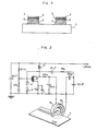
- FIG. 1 represents an enlarged sectional view of the support, at the level of two areas, and
- FIG. 2 is an electrical diagram of the HF device supplying the thermal erasure device
- the information carrier is in the form of a rectangular card or ticket cut from an insulating and non-magnetic material, such as for example epoxy or polyimide glass, material of the Kapton brand or Nomex brand paper. All these materials, the list of which is not exhaustive, are. chosen according to their resistance to temperature and their good mechanical characteristics allowing them to circulate in magnetic readers without premature wear.
- On one face of this support 1 are arranged the distinct fields of magnetizable information. These areas are in the form of small rods with a length of the order of 4 mm for a width of about 0.6 mm, for example. They are uniformly distributed one after the other on one or more parallel lines.
- Each area has a copper sub-layer 2, the thickness of which, which can vary from 5 ⁇ m to 40 ⁇ m, is sufficient for large induced currents to develop there.
- a copper sublayer On this copper sublayer are successively deposited, for example by electrolysis, a first diffusing layer 4 such as indium, bismuth or a lead-tin alloy, then a magnetizable layer 3, such as nickel cobalt, then a second diffusing layer 4.
- These layers each have a thickness of from 0 0 500 A to 1000 A approximately. This sandwich arrangement is the most favorable for the dispersion of the diffusing agent in the magnetic layer during a rise in temperature.
- the creation of such an information medium can be advantageously made from elements of standard plates already covered with a thickness of copper of 17.5 or 35 ⁇ m. After the electrolysis of the various elements constituting the memory, the superfluous copper is then removed by etching.
- FIG. 2 represents an HF generator allowing the temperature rise and the destruction of the magnetism domain by domain.
- Its oscillation frequency is 13.5 MHz which is the frequency authorized in the industry to meet standards on the emission of radio interference. Its consumption under 20 Volts varies from 0.3 A, when there is no domain in the air gap of the heating head, to 0.6 A when there is a domain.
- It essentially comprises a field effect transistor 10, a ferrite coil 12 of 47 u Henry, two Zener diodes 11 in series and head to tail to limit overvoltages, and a coil 13 of 5 turns surrounding a ferrite toroid 14.
- Des clearances 14a refine the air gap, of the order of 0.4 mm, to concentrate the lines of force of the magnetic field in the dimensions of a domain.
- the winding 13 can advantageously extend over the clearances 14a, as close as possible to the air gap, which minimizes the losses. Under these conditions, the destruction of an information domain can be done in a period of the order of a second.
- the information medium as described and illustrated, used with an HF heating head as described, makes it possible to produce credit cards or tickets usable in payment devices whose cost is variable. It is particularly suitable for paying telephone charges in places where the storage of money presents a risk.
Landscapes
- Engineering & Computer Science (AREA)
- Physics & Mathematics (AREA)
- General Physics & Mathematics (AREA)
- Theoretical Computer Science (AREA)
- Business, Economics & Management (AREA)
- Computer Networks & Wireless Communication (AREA)
- Microelectronics & Electronic Packaging (AREA)
- Computer Security & Cryptography (AREA)
- Accounting & Taxation (AREA)
- Strategic Management (AREA)
- General Business, Economics & Management (AREA)
- Credit Cards Or The Like (AREA)
- Magnetic Record Carriers (AREA)
Abstract
Description
La présente invention concerne un support d'informations comportant des éléments de mémoire magnétique, réalisés par des couches successives de matériaux magnétiques et de matériaux diffusants, desctructibles de façon irréversible par élévation de température.The present invention relates to an information medium comprising magnetic memory elements, produced by successive layers of magnetic materials and diffusing materials, which are irreversibly destructible by rise in temperature.
On connaît déjà, tel que décrit dans la demande de brevet français n° 80 11 320 au nom de la demanderesse, un support d'informations revêtu sur toute une face d'une couche mince de cuivre sur laquelle sont déposés les éléments de mémoire thermodestructible. Pour obtenir la destruction du magnétisme dans un laps de temps suffisamment court, ces éléments de mémoire, ou domaines d'informations, doivent être portés à une température de l'ordre de 250° à 300°C. Plusieurs procédés permettent d'obtenir ce résultat.We already know, as described in French patent application No. 80 11 320 in the name of the applicant, an information carrier coated on one side with a thin layer of copper on which are deposited the thermodestructible memory elements . To obtain the destruction of magnetism in a sufficiently short period of time, these memory elements, or areas of information, must be brought to a temperature of the order of 250 ° to 300 ° C. Several methods make it possible to obtain this result.
Les domaines peuvent être chauffés par contacts avec une ou plusieurs résistances, par exemple des résistances en couche épaisse, déposées sur un support en steatite ou alumine. Ils peuvent également être soumis au flux lumineux d'une lampe, concentré par des moyens optiques, ou chauffé directement par effet Joule.The domains can be heated by contact with one or more resistors, for example resistors in thick layer, deposited on a support in steatite or alumina. They can also be subjected to the luminous flux of a lamp, concentrated by optical means, or heated directly by the Joule effect.
Tous ces procédés présentent des inconvénients. Soit ils nécessitent des sources d'énergie importantes, de plusieurs dizaines de watts, soit ils brûlent la surface du support ce qui provoque l'encrassement des têtes de lecture magnétiques lors de l'exploitation du support d'information.All of these methods have drawbacks. Either they require significant energy sources, of several tens of watts, or they burn the surface of the support which causes the fouling of the magnetic reading heads during the exploitation of the information support.
Pour éviter ces inconvénients, la demanderesse a songé à ne concentrer l'énergie qu'au sein même de chaque domaine ce qui peut être obtenu par le procédé de chauffage par hautes fréquences et l'invention a pour objet un support d'informations adapté à ce procédé.To avoid these drawbacks, the applicant has thought of concentrating energy only within each domain, which can be obtained by the high frequency heating process, and the subject of the invention is an information medium adapted to this process.
A cet effet, le support d'informations objet de l'invention est caractérisé en ce que sur au moins une face du support, découpé dans un matériau isolant et amagnétique, il est prévu une succession de domaines, comprenant une couche en métal conducteur de l'électricité, recouverte par un élément de mémoire magnétique thermodestructible.To this end, the information medium which is the subject of the invention is characterized in that on at least one face of the medium, cut from an insulating and non-magnetic material, a succession of fields is provided, comprising a layer of conductive metal electricity, covered by a thermodestructible magnetic memory element.
L'expérience a montré que les couches, constituant un élément mémoire, ont une résistivité trop élevée pour qu'ils s'y développe un courant induit suffisant. Aussi, chaque domaine d'information est constitué par une sous couche en métal bon conducteur de l'électricité dont l'épaisseur est relativement importante par rapport aux couches magnétiques et diffusantes. En effet, dans la pratique, seuls les courants induits dans la sous couche conductrice interviennent dans l'élévation de température des domaines lorsque ceux-ci sont soumis à un champ magnétique haute fréquence.Experience has shown that the layers constituting a memory element have too high a resistivity for them to develop a sufficient induced current. Also, each information domain is constituted by an under layer of metal which is a good conductor of electricity, the thickness of which is relatively large compared to the magnetic and diffusing layers. Indeed, in practice, only the currents induced in the conductive sublayer intervene in the temperature rise of the domains when these are subjected to a high frequency magnetic field.
Le dispositif de chauffe consiste en un circuit générateur HF classique, alimentant une bobine disposée autour d'une ferrite torique, fendue. Le maximum de rendement, c'est-à-dire de lignes de champ magnétique actives traversant un domaine, est obtenu lorsque le support d'informations est introduit dans la fente de la ferrite jouant le rôle d'entrefer. Dans ces conditions on peut estimer que la perte P, c'est-à-dire l'énergie dissipée dans la partie métallique d'un domaine, est de la forme :
- où D représente la largeur d'un domaine,
- e " l'épaisseur de métal d'un domaine,
- F " la fréquence du générateur,
- B " l'induction,
- f " la résistivité du métal utilisé.
- where D represents the width of a domain,
- e "the thickness of metal of a field,
- F "the generator frequency,
- B "induction,
- f "the resistivity of the metal used.
Le dessin annexé illustre à titre d'exemple un mode de réalisation d'un support d'information, ainsi que de son dispositif de chauffe, conforme à la présente invention.The accompanying drawing illustrates by way of example a method of production of an information medium, as well as its heating device, in accordance with the present invention.
La figure 1 représente une vue en coupe, agrandie, du support, au niveau de deux domaines, etFIG. 1 represents an enlarged sectional view of the support, at the level of two areas, and
La figure 2 est un schéma électrique du dispositif HF alimentant le dispositif d'effacement thermiqueFIG. 2 is an electrical diagram of the HF device supplying the thermal erasure device
Tel que représenté, figure 1, le support d'informations se présente sous la forme d'une carte ou ticket rectangulaire découpé dans un matériau isolant et amagnétique, tel que par exemple du verre époxy ou polyimide, du matériau de la marque Kapton ou du papier de la marque Nomex. Tous ces matériaux, dont la liste n'est pas limitative, sont. choisis en fonction de leur tenue à la température et de leurs bonnes caractéristiques mécaniques leur permettant de circuler dans des lecteurs magnétiques sans usure prématurée. Sur une face de ce support 1 sont disposés les domaines distincts d'informations magnétisables. Ces domaines se présentent sous la forme de petits bâtonnets d'une longueur de l'ordre de 4 mm pour une largeur de 0,6 mm environ, à titre d'exemple. Ils sont uniformément répartis les uns à la suite des autres sur une ou plusieurs lignes parallèles. Chaque domaine comporte une sous couche de cuivre 2, dont l'épaisseur, qui peut varier de 5 r à 40 µm, est suffisante pour que puisse s'y développer des courants induits importants. Sur cette sous couche de cuivre sont successivement déposées, par exemple par électrolyse, une première couche diffusante 4 telle que de l'indium, bismuth ou un alliage de plomb-étain, puis une couche magnétisable 3, telle que du nickel cobalt, puis une seconde couche diffusante 4. Ces couches ont chacune une épaisseur de 0 0 500 A à 1000 A environ. Cette disposition en sandwich est la plus favorable pour la dispersion du diffusant dans la couche magnétique lors d'une élévation de température.As shown in Figure 1, the information carrier is in the form of a rectangular card or ticket cut from an insulating and non-magnetic material, such as for example epoxy or polyimide glass, material of the Kapton brand or Nomex brand paper. All these materials, the list of which is not exhaustive, are. chosen according to their resistance to temperature and their good mechanical characteristics allowing them to circulate in magnetic readers without premature wear. On one face of this
La réalisation d'un tel support d'informations peut être avantageusement faite à partir d'éléments de plaques standards déjà recouvertes d'une épaisseur de cuivre de 17,5 ou 35 ym. Après l'électrolyse des divers éléments constituant la mémoire, le cuivre superflu est alors enlevé par gravure.The creation of such an information medium can be advantageously made from elements of standard plates already covered with a thickness of copper of 17.5 or 35 μm. After the electrolysis of the various elements constituting the memory, the superfluous copper is then removed by etching.
La figure 2 représente un générateur HF permettant l'élévation de température et la destruction du magnétisme domaine par domaine. Sa fréquence d'oscillation est de 13,5 MHz qui est la fréquence autorisée dans l'industrie pour répondre aux normes sur l'émission des parasites radioélectriques. Sa consommation sous 20 Volts varie de 0,3 A, lorsqu'il n'y a pas de domaine dans l'entrefer de la tête de chauffe, à 0,6 A lors de la présence d'un domaine.FIG. 2 represents an HF generator allowing the temperature rise and the destruction of the magnetism domain by domain. Its oscillation frequency is 13.5 MHz which is the frequency authorized in the industry to meet standards on the emission of radio interference. Its consumption under 20 Volts varies from 0.3 A, when there is no domain in the air gap of the heating head, to 0.6 A when there is a domain.
Il comprend essentiellement un transistor à effet de champ 10, une bobine en ferrite 12 de 47 uhenry, deux diodes Zener 11 en série et tête bêche pour limiter les surtensions, et un bobinage 13 de 5 spires entourant un tore en ferrite 14. Des dégagements 14a affinent l'entrefer, de l'ordre de 0,4 mm, pour concentrer les lignes de forces du champ magnétique dans les dimensions d'un domaine.It essentially comprises a
Le bobinage 13 peut avantageusement s'étendre sur les dégagements 14a, au plus près de l'entrefer, ce qui minimise les pertes. Dans ces conditions, la destruction d'un domaine d'informations peut se faire en un laps de temps de l'ordre de la seconde.The winding 13 can advantageously extend over the clearances 14a, as close as possible to the air gap, which minimizes the losses. Under these conditions, the destruction of an information domain can be done in a period of the order of a second.
Le support d'informations tel que décrit et illustré, utilisé avec une tête de chauffage HF telle que décrite, permet de réaliser des cartes de crédit ou des tickets utilisables dans des dispositifs de paiement dont le coût est variable. Il se prête notamment particulièrement bien au paiement des taxes téléphoniques en des lieux où le stockage d'argent présente un risque.The information medium as described and illustrated, used with an HF heating head as described, makes it possible to produce credit cards or tickets usable in payment devices whose cost is variable. It is particularly suitable for paying telephone charges in places where the storage of money presents a risk.
Claims (3)
Applications Claiming Priority (2)
| Application Number | Priority Date | Filing Date | Title |
|---|---|---|---|
| FR8213149A FR2530834A1 (en) | 1982-07-26 | 1982-07-26 | THERM INFORMATION SUPPORT |
| FR8213149 | 1982-07-26 |
Publications (1)
| Publication Number | Publication Date |
|---|---|
| EP0101344A1 true EP0101344A1 (en) | 1984-02-22 |
Family
ID=9276390
Family Applications (1)
| Application Number | Title | Priority Date | Filing Date |
|---|---|---|---|
| EP83401444A Withdrawn EP0101344A1 (en) | 1982-07-26 | 1983-07-12 | Information carrier with thermo-destructible magnetic memory elements |
Country Status (3)
| Country | Link |
|---|---|
| EP (1) | EP0101344A1 (en) |
| JP (1) | JPS5938926A (en) |
| FR (1) | FR2530834A1 (en) |
Cited By (1)
| Publication number | Priority date | Publication date | Assignee | Title |
|---|---|---|---|---|
| WO1995020203A1 (en) * | 1994-01-24 | 1995-07-27 | TELECOMUNICAÇõES BRASILEIRAS S/A - TELEBRÁS | Improved debiting method for inductive prepayment cards |
Families Citing this family (2)
| Publication number | Priority date | Publication date | Assignee | Title |
|---|---|---|---|---|
| JP2543938B2 (en) * | 1988-02-16 | 1996-10-16 | 共同印刷株式会社 | Magnetic recording media |
| JP4794201B2 (en) | 2005-04-25 | 2011-10-19 | 株式会社松風 | 2 paste type glass ionomer cement |
Citations (2)
| Publication number | Priority date | Publication date | Assignee | Title |
|---|---|---|---|---|
| FR2310599A1 (en) * | 1975-05-06 | 1976-12-03 | Landis & Gyr Ag | DISTINCTIVE MAGNETISABLE CARD |
| EP0040561A2 (en) * | 1980-05-21 | 1981-11-25 | Crouzet | Thermally destructible magnetic memory element |
-
1982
- 1982-07-26 FR FR8213149A patent/FR2530834A1/en active Granted
-
1983
- 1983-07-12 EP EP83401444A patent/EP0101344A1/en not_active Withdrawn
- 1983-07-26 JP JP13527283A patent/JPS5938926A/en active Pending
Patent Citations (2)
| Publication number | Priority date | Publication date | Assignee | Title |
|---|---|---|---|---|
| FR2310599A1 (en) * | 1975-05-06 | 1976-12-03 | Landis & Gyr Ag | DISTINCTIVE MAGNETISABLE CARD |
| EP0040561A2 (en) * | 1980-05-21 | 1981-11-25 | Crouzet | Thermally destructible magnetic memory element |
Cited By (2)
| Publication number | Priority date | Publication date | Assignee | Title |
|---|---|---|---|---|
| WO1995020203A1 (en) * | 1994-01-24 | 1995-07-27 | TELECOMUNICAÇõES BRASILEIRAS S/A - TELEBRÁS | Improved debiting method for inductive prepayment cards |
| US5834757A (en) * | 1994-01-24 | 1998-11-10 | Telecomunicacoes Brasileiras S/A Telebras | Debiting method for inductive prepayment cards |
Also Published As
| Publication number | Publication date |
|---|---|
| JPS5938926A (en) | 1984-03-03 |
| FR2530834A1 (en) | 1984-01-27 |
| FR2530834B1 (en) | 1984-12-14 |
Similar Documents
| Publication | Publication Date | Title |
|---|---|---|
| FR2621147A1 (en) | INTEGRATED CIRCUIT BOARD OF CONTACTLESS TYPE AND DEVICE FOR READING / WRITING CONTACTLESS TYPE CARDS | |
| US5025341A (en) | Thermo-magnetic recording head | |
| WO2008065127A2 (en) | Miniature transponder and identification system including said transponder and a suitable reader | |
| EP1116179B1 (en) | Contactless card comprising inhibiting means | |
| EP0917101B1 (en) | Antenna coil with reduced electric field | |
| FR2800518A1 (en) | HIGH INDUCTANCE COUPLING ANTENNA | |
| EP0040561B1 (en) | Thermally destructible magnetic memory element | |
| EP0616484A1 (en) | Magnetoresistive transducer und manufacturing method | |
| EP0446107B1 (en) | Transmission system for electrical energy, in the microwave field, with gyromagnetic effect, such as a circulator, isolator or filter | |
| EP0013192B1 (en) | Data processing system and control device for data cards utilizing magnetic bubble elements | |
| EP0101344A1 (en) | Information carrier with thermo-destructible magnetic memory elements | |
| FR2458396A1 (en) | THERMAL PRINTING HEAD | |
| FR2745928A1 (en) | NON-CONTACT INFORMATION EXCHANGE DEVICE WITH AN ELECTRONIC TICKET | |
| FR2610754A1 (en) | DATA EXCHANGE TRANSDUCER FOR INTEGRATED CIRCUIT BOARD | |
| FR2627270A1 (en) | DEVICE AND METHOD FOR FERRITE CORE TORQUE SLAPPER DETONATOR | |
| FR2556493A1 (en) | Electromagnetic winding and transformer containing such a winding | |
| EP0203952B1 (en) | Ironless solenoidal magnet | |
| EP1260821B1 (en) | Detectiont transformer for a differential protection device and protection device using such a transformer | |
| EP0771135B1 (en) | Inductive Litz wire winding used in an induction cooking apparatus | |
| FR2828570A1 (en) | Production of a contact-less chip support comprises laminating an insulating film on a micro-module film, laminating an adhesive film on the micro-module film, cutting the micro-module and applying an antenna to each micro-module | |
| FR2777141A1 (en) | Transponder circuit design | |
| FR3021839A1 (en) | METHOD FOR MANUFACTURING A CONFIGURABLE ELECTRICAL COMPONENT | |
| EP0667628B1 (en) | Superconductive bobbin with general transition | |
| EP0206879B1 (en) | Broad frequency band magnetic field detector | |
| WO1990010320A1 (en) | Process for producing a flat connection |
Legal Events
| Date | Code | Title | Description |
|---|---|---|---|
| PUAI | Public reference made under article 153(3) epc to a published international application that has entered the european phase |
Free format text: ORIGINAL CODE: 0009012 |
|
| AK | Designated contracting states |
Designated state(s): AT BE CH DE GB IT LI LU NL SE |
|
| 17P | Request for examination filed |
Effective date: 19840329 |
|
| STAA | Information on the status of an ep patent application or granted ep patent |
Free format text: STATUS: THE APPLICATION IS DEEMED TO BE WITHDRAWN |
|
| 18D | Application deemed to be withdrawn |
Effective date: 19850919 |
|
| RIN1 | Information on inventor provided before grant (corrected) |
Inventor name: VERGUES, JACQUES Inventor name: MORILLE, ROBERT |