EP0100572A2 - Electrically erasable PROM-cell - Google Patents
Electrically erasable PROM-cell Download PDFInfo
- Publication number
- EP0100572A2 EP0100572A2 EP83201066A EP83201066A EP0100572A2 EP 0100572 A2 EP0100572 A2 EP 0100572A2 EP 83201066 A EP83201066 A EP 83201066A EP 83201066 A EP83201066 A EP 83201066A EP 0100572 A2 EP0100572 A2 EP 0100572A2
- Authority
- EP
- European Patent Office
- Prior art keywords
- floating gate
- gate
- region
- channel region
- conductivity type
- Prior art date
- Legal status (The legal status is an assumption and is not a legal conclusion. Google has not performed a legal analysis and makes no representation as to the accuracy of the status listed.)
- Granted
Links
- 239000000463 material Substances 0.000 claims description 4
- 230000005641 tunneling Effects 0.000 abstract description 30
- 239000000758 substrate Substances 0.000 abstract description 23
- 230000007423 decrease Effects 0.000 abstract description 2
- 230000005684 electric field Effects 0.000 description 8
- ZOXJGFHDIHLPTG-UHFFFAOYSA-N Boron Chemical compound [B] ZOXJGFHDIHLPTG-UHFFFAOYSA-N 0.000 description 4
- VYPSYNLAJGMNEJ-UHFFFAOYSA-N Silicium dioxide Chemical compound O=[Si]=O VYPSYNLAJGMNEJ-UHFFFAOYSA-N 0.000 description 4
- 229910052796 boron Inorganic materials 0.000 description 4
- 239000007943 implant Substances 0.000 description 3
- 229910052785 arsenic Inorganic materials 0.000 description 2
- RQNWIZPPADIBDY-UHFFFAOYSA-N arsenic atom Chemical compound [As] RQNWIZPPADIBDY-UHFFFAOYSA-N 0.000 description 2
- 239000002800 charge carrier Substances 0.000 description 2
- 239000002019 doping agent Substances 0.000 description 2
- 230000000694 effects Effects 0.000 description 2
- 230000001939 inductive effect Effects 0.000 description 2
- 229910021420 polycrystalline silicon Inorganic materials 0.000 description 2
- 229920005591 polysilicon Polymers 0.000 description 2
- 239000004065 semiconductor Substances 0.000 description 2
- 235000012239 silicon dioxide Nutrition 0.000 description 2
- 239000000377 silicon dioxide Substances 0.000 description 2
- 230000015572 biosynthetic process Effects 0.000 description 1
- 239000000969 carrier Substances 0.000 description 1
- 230000008878 coupling Effects 0.000 description 1
- 238000010168 coupling process Methods 0.000 description 1
- 238000005859 coupling reaction Methods 0.000 description 1
- 238000009792 diffusion process Methods 0.000 description 1
- 239000012212 insulator Substances 0.000 description 1
- 238000009877 rendering Methods 0.000 description 1
- 229910052710 silicon Inorganic materials 0.000 description 1
- 239000010703 silicon Substances 0.000 description 1
Images
Classifications
-
- G—PHYSICS
- G11—INFORMATION STORAGE
- G11C—STATIC STORES
- G11C16/00—Erasable programmable read-only memories
- G11C16/02—Erasable programmable read-only memories electrically programmable
- G11C16/04—Erasable programmable read-only memories electrically programmable using variable threshold transistors, e.g. FAMOS
- G11C16/0408—Erasable programmable read-only memories electrically programmable using variable threshold transistors, e.g. FAMOS comprising cells containing floating gate transistors
- G11C16/0441—Erasable programmable read-only memories electrically programmable using variable threshold transistors, e.g. FAMOS comprising cells containing floating gate transistors comprising cells containing multiple floating gate devices, e.g. separate read-and-write FAMOS transistors with connected floating gates
-
- H—ELECTRICITY
- H01—ELECTRIC ELEMENTS
- H01L—SEMICONDUCTOR DEVICES NOT COVERED BY CLASS H10
- H01L29/00—Semiconductor devices adapted for rectifying, amplifying, oscillating or switching, or capacitors or resistors with at least one potential-jump barrier or surface barrier, e.g. PN junction depletion layer or carrier concentration layer; Details of semiconductor bodies or of electrodes thereof ; Multistep manufacturing processes therefor
- H01L29/66—Types of semiconductor device ; Multistep manufacturing processes therefor
- H01L29/68—Types of semiconductor device ; Multistep manufacturing processes therefor controllable by only the electric current supplied, or only the electric potential applied, to an electrode which does not carry the current to be rectified, amplified or switched
- H01L29/76—Unipolar devices, e.g. field effect transistors
- H01L29/772—Field effect transistors
- H01L29/78—Field effect transistors with field effect produced by an insulated gate
- H01L29/788—Field effect transistors with field effect produced by an insulated gate with floating gate
- H01L29/7881—Programmable transistors with only two possible levels of programmation
- H01L29/7883—Programmable transistors with only two possible levels of programmation charging by tunnelling of carriers, e.g. Fowler-Nordheim tunnelling
-
- H—ELECTRICITY
- H10—SEMICONDUCTOR DEVICES; ELECTRIC SOLID-STATE DEVICES NOT OTHERWISE PROVIDED FOR
- H10B—ELECTRONIC MEMORY DEVICES
- H10B69/00—Erasable-and-programmable ROM [EPROM] devices not provided for in groups H10B41/00 - H10B63/00, e.g. ultraviolet erasable-and-programmable ROM [UVEPROM] devices
Definitions
- This invention relates to a memory device, comprising: a body of semiconductive material of first conductivity type; first and second regions of second conductivity type spaced apart in said body by a first channel region; a floating gate overlying said first channel region; a first insulating layer separating said floating gate from said first channel region and having a portion which overlies a part of said first channel region and is thinner than the remainder thereof; a control gate overlying said floating gate; a second insulating layer of greater thickness than the thin portion of said first insulating layer separating said control gate from said floating gate.
- MOS memory devices which are constructed with an electrically isolated floating gate between the control gate and the semiconductive body. By inducing a high enough electric field of the proper polarity between the floating gate and the' semiconductive body, charge carriers can tunnel through a thin insulator from the semiconductor body to the floating gate to program the device to one binary state. By inducing an electric field of the opposite polarity between the floating gate and the semiconductive body, charge carriers can be removed from the floating gate to erase the data or cause the device to revert to its other binary state.
- the tunneling oxide between the floating gate and the substrate must be very thin, for example about 100 angstroms or less and about one-tenth the thickness of the oxide between the floating gate and the control gate. If the two gates were of the same area, most of the induced electric field would be developed across the thicker inter- gate oxide and very little electric field would appear across the tunneling oxide where it is needed.
- the overlap area between the control gate and the floating gate must be very large relative to the tunneling area. The overlap area must be larger than that required to just compensate for the large thickness ratio of the two oxide layers. For the example given above, the overlap area must be about 15 times the area of the tunneling oxide.
- a body of semiconductive material of first conductivity type is provided with first and second regions of second conductivity type that are spaced apart by a first channel region.
- a third region of second conductivity type is spaced apart in the body from the second region by a second channel region.
- a floating gate overlies both the first and second channel regions.
- a first insulating layer separates the floating gate from the first and second channel regions.
- the first insulating layer has a portion which overlies a part of the first channel region that is thinner than the remainder thereof.
- the thin insulating layer portion constitutes a window through which charge tunneling can occur between the floating gate and the semiconductive'body.
- a control gate overlies the floating gate and is separated from the floating gate by a second insulating layer that is thicker than the thin portion of the first insulating layer.
- the first and second channel regions have an additional surface doping of first conductivity type and the floating gate has a doping of first conductivity type which together act to raise the virgin state threshold voltage of the first and second channel regions.
- the areas of the floating gate and the control gate and the thickness of the first and second insulating layer are so proportioned that when a programming voltage is applied between the control gate and the semiconductive body, an inversion layer is produced in the first channel region, thereby rendering the capacitance between the floating gate and the control gate substantially equal to the capacitance between the floating gate and the semiconductive body.
- the electric field thus produced across the thin insulating layer portion is not sufficient to produce any significant tunneling action therethrough to the floating gate, the floating gate voltage does not change, and the threshold voltage of the device does not change from the virgin state.
- the floating gate when an erase voltage of opposite polarity is applied between the control gate and the first region of second conductivity type, such as the drain region, there is no inversion layer produced in the first channel region and the capacitance between the floating gate and the semiconductive body is merely that which is limited to the small side diffused area of the drain region which is overlapped by the floating gate.
- the floating gate thus receives only a small proportion of the erase voltage, but a high voltage difference and high electric field is produced across the thin insulating layer. The high electric field is sufficient to produce tunneling from the floating gate to the drain region, thereby raising the floating gate to a more positive voltage and driving the threshold voltage to a negative value.
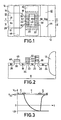
- Figs. 1 and 2 show a top plan view and a cross- sectional view, respectively, of an electrically erasable programmable read-only memory (EEPROM) cell constructed according to the invention.
- a semiconductive body or substrate 8 of monocrystalline semiconductive material, such as silicon, is provided with an active area 10 surrounded by areas of field oxide 12. The boundaries between the field oxide 12 and the active area 10 are denoted by two heavy lines 14 and 16.
- the cell is an n-channel device and so the substrate is shown as P-type, or first conductivity type.
- Within the top surface of the substrate 10 there are formed several laterally spaced regions of second conductivity type.
- a first region 18 of second conductivity type and a second region 20 of second conductivity type are spaced apart by a first channel region 22.
- a third region 24 of second conductivity type is spaced from the second region 20 by a second channel region 26.
- a fourth region 28 of second conductivity type is spaced from the first region 18 by a third channel region 30. All of the regions 18, 20, 24, 28 are heavily doped N-type conductivity regions, and as such are dsignated N+.
- the three channel regions 22, 26, 30 are aligned lengthwise along a common linear axis.
- a rectangularly annular floating gate 32 overlies both the first and second channel regions 22 and 26 respectively.
- the floating gate 32 is separated from a part of the first channel region 22 by a thin oxide region 34 and is separated from the remainder of the first channel region 22 by a thicker oxide layer 36.
- the thin oxide region 34 is 70 to 100 angstroms thick and the thicker oxide layer 36 is about 1000 angstroms thick.
- the thicker oxide layer 38 of the same thickness as the oxide layer 36 also separates the floating gate 32 from the second channel region 26.
- the annular floating gate 32 extends over the entire width of the first and second channel regions 22 and 26 and also extends partly over the field oxide 12, as shown in Fig. 1.
- a control gate 40 overlies the floating gate 32 and has a rectangular opening 42 over the second region 20 coinciding with a similar opening in the floating gate 32.
- the control gate 40 extends vertically in both directions to other similar cells which are not shown.
- the control gate 40 is separated from the floating gate by an insulating layer 44, such as thermally grown silicon dioxide.
- the insulating layer 44 is approximately 800 angstroms thick.
- a select gate 46 extends over the third channel region 30.
- the select gate 46 extends over the entire width of the third channel region 30 and also extends in both directions to other cells parallel to the control gate 40.
- the select gate 46 is separated from the third channel region 30 by an insulating layer 48, such as thermal silicon dioxide.
- the insulating layer 48 is about 700 angstroms thick.
- the select gate 46 and the N+ regions 18 and 28 separated by the third channel region 30 form a select transistor for selecting the memory cell.
- the N+ region 28 may be called the bit line, and the select gate 46 may also be called the select line or word line.
- the control gate 40 and the select gate 46 may be made of polysilicon and doped N-type or P-type to render them conductive.
- the floating gate 32 is made of polysilicon and is doped P-type the same as the substrate 10, such as with boron.
- the first and second channel regions 22 and 26 also have an additional P-type doping of boron or the like, which may comprise an additional implant.
- the P-type doping of the channel regions 22 and 26 and of the floating gate 32 act to raise the virgin state threshold voltage of the memory cell.
- the virgin state threshold voltage of the memory cell should be at least 3 or 4 volts positive.
- the virgin state threshold voltage is the minimum voltage which can be applied to the control gate 40 to cause an inversion in the channel region 26, in the absence of charge on the floating gate 32 caused by tunneling.
- Channel region 22, of course, has a lower virgin state threshold because of the thin oxide region 34.
- the ratio of the capacitance between the floating gate and the control gate and the capacitance between the floating gate and the substrate is greater than 1, say 2.5. This is achieved by increasing the area of overlap between the control gate and the floating gate to about 30 times the area of the thin tunneling oxide.
- the virgin threshold may be 1 or 2 volts positive. Thus, if 20 volts positive is applied to the control gate to program the cell, the floating gate will receive 14 volts, which is substantially above the 10 volts required for tunneling through 100 angstroms of oxide.
- the present invention does not use an arsenic or N-type implant beneath the tunneling oxide, but instead adds an opposite type dopant, v such as boron, which is of the same conductivity type as the substrate. Furthermore, the floating gate is also provided with a similar boron or P-type doping. The effect of these two measures is to raise the virgin state threshold voltage of the memory cell above that normally present in the prior art devices. Typically, the virgin state threshold voltage of the memory cell according to the invention is at least 3 volts and preferably about 4 volts.
- the area of the overlap between the control gate and the floating gate which also is the area of the interpoly oxide, is one half of the one that is present in prior art devices, which is only 15 times the area of the tunneling oxide. Accordingly, with the interpoly oxide being about 7.5 to 10 times the thickness of the thin tunneling oxide, the ratio of the relevant two capacitances is about one. That is, the capacitance between the floating gate and the control gate is about equal to the capacitance between the floating gate and the substrate.
- a voltage of 20 volts positive is applied to the control gate 40 and the substrate 10 is grounded. Because the capacitance ratio is 1, only 10 volts will be induced on the floating gate 32.10 volts on the floating gate 32 is sufficient to cause inversion in the first channel region 22 beneath the thin oxide layer 34 but it is not sufficient to cause any significant tunneling of electrons to the floating gate 32.
- the floating voltage gate 32 will change little, if at all, and the threshold voltage of thememory device will remain the same, which is the virgin state threshold voltage of 4 volts, for example, assuming the state of the memory cell prior to programming was the virgin state.
- the threshold voltage V T duringprogramming (interval P 1 ) is shown as remaining flat at a value of 4 volts equal to the virgin threshold V o .
- the voltage will divide so that most of it will be induced across the small capacitance between the floating gate 32 and the drain region 18. Only three volts positive or so will appear on the floating gate 32, making the voltage difference 13 volts. 13 volts is sufficient to produce effective tunneling action from the floating gate 32 to the drain region 18. Removing electrons from the floating gate 32 causes the potential on the floating gate 32 to rise positively and the threshold voltage to decrease or more in a negative direction. Thus in Fig. 3 the threshold voltage V T of the memory cell is seen to drop by 6 volts to minus 2 volts (interval E).
- the substrate 10 When it is time to reprogram the memory cell, the substrate 10 is grounded and the control gate voltage is again raised to 20 volts positive.
- the threshold voltage V T rises again to a level equal to the virgin state threshold value as before (interval P 2 ) because +3V worth of charge on the flating gate raises the floating gate voltage to +13V which causes electron tunneling into the gate to cancel the positive charges in the floating gate.
- the capacitance ratio is reduced to the extent that little or no tunneling action occurs during programming.
- the effective capacitance ratio is reduced even further to.an extent that an opposite polarity voltage applied between the substrate and the control gate causes very efficient tunneling action from the floating gate to the drain region 18.
- the threshold voltage window which is the difference in threshold voltage G-between the value at programming and the value at erase, is maintained sufficiently high, despite the absence of tunneling action during programming.
- the reduced area of overlap between the control gate and floating gate makes it possible to reduce the size of EEPROMS having capacity of 32K bits and higher.
Abstract
Description
- This invention relates to a memory device, comprising: a body of semiconductive material of first conductivity type; first and second regions of second conductivity type spaced apart in said body by a first channel region; a floating gate overlying said first channel region; a first insulating layer separating said floating gate from said first channel region and having a portion which overlies a part of said first channel region and is thinner than the remainder thereof; a control gate overlying said floating gate; a second insulating layer of greater thickness than the thin portion of said first insulating layer separating said control gate from said floating gate.
- Metal-oxide-semiconductor (MOS) memory devices are known which are constructed with an electrically isolated floating gate between the control gate and the semiconductive body. By inducing a high enough electric field of the proper polarity between the floating gate and the' semiconductive body, charge carriers can tunnel through a thin insulator from the semiconductor body to the floating gate to program the device to one binary state. By inducing an electric field of the opposite polarity between the floating gate and the semiconductive body, charge carriers can be removed from the floating gate to erase the data or cause the device to revert to its other binary state.
- An electrically erasable programmable read-only memory (EEPROM) of the MOS kind employing a floating gate and a tunneling oxide is disclosed in US Patent 4,203)158. Since the floating gate in this type of device is electrically isolated from the outside, the programming and erase voltage is applied between the accessible control gate and the substrate, and the tunneling electric field is induced between the floating gate and the substrate through capacitive coupling. There are two capacitances associated with the floating gate. One is the capacitance between the floating gate and the substrate, and the other is the capacitance between the floating gate and the control gate. These two capacitances form a voltage.,divider across which the applied voltage divides inversely as the capacitance.
- In order to provide effective tunneling action with reasonably low supply voltage in the neighborhood of 20 volts, the tunneling oxide between the floating gate and the substrate must be very thin, for example about 100 angstroms or less and about one-tenth the thickness of the oxide between the floating gate and the control gate. If the two gates were of the same area, most of the induced electric field would be developed across the thicker inter- gate oxide and very little electric field would appear across the tunneling oxide where it is needed. For effective tunneling action in the program mode, the overlap area between the control gate and the floating gate must be very large relative to the tunneling area. The overlap area must be larger than that required to just compensate for the large thickness ratio of the two oxide layers. For the example given above, the overlap area must be about 15 times the area of the tunneling oxide. This large area requirement makes it rather difficult to fabricate high density EEPROMS that have a capacity of more than 16K bits and yet are not unduly bulky. There is a great need for a new EEPROM design of reduced physical size which also can be programmed and erased with relatively low voltages currently in use.
- In accordance with the invention, a body of semiconductive material of first conductivity type is provided with first and second regions of second conductivity type that are spaced apart by a first channel region. A third region of second conductivity type is spaced apart in the body from the second region by a second channel region. A floating gate overlies both the first and second channel regions. A first insulating layer separates the floating gate from the first and second channel regions. The first insulating layer has a portion which overlies a part of the first channel region that is thinner than the remainder thereof. The thin insulating layer portion constitutes a window through which charge tunneling can occur between the floating gate and the semiconductive'body. A control gate overlies the floating gate and is separated from the floating gate by a second insulating layer that is thicker than the thin portion of the first insulating layer.
- The first and second channel regions have an additional surface doping of first conductivity type and the floating gate has a doping of first conductivity type which together act to raise the virgin state threshold voltage of the first and second channel regions. The areas of the floating gate and the control gate and the thickness of the first and second insulating layer are so proportioned that when a programming voltage is applied between the control gate and the semiconductive body, an inversion layer is produced in the first channel region, thereby rendering the capacitance between the floating gate and the control gate substantially equal to the capacitance between the floating gate and the semiconductive body. The electric field thus produced across the thin insulating layer portion is not sufficient to produce any significant tunneling action therethrough to the floating gate, the floating gate voltage does not change, and the threshold voltage of the device does not change from the virgin state.
- However, when an erase voltage of opposite polarity is applied between the control gate and the first region of second conductivity type, such as the drain region, there is no inversion layer produced in the first channel region and the capacitance between the floating gate and the semiconductive body is merely that which is limited to the small side diffused area of the drain region which is overlapped by the floating gate. The floating gate thus receives only a small proportion of the erase voltage, but a high voltage difference and high electric field is produced across the thin insulating layer. The high electric field is sufficient to produce tunneling from the floating gate to the drain region, thereby raising the floating gate to a more positive voltage and driving the threshold voltage to a negative value.
-
- Fig. 1 is a top plan view of a memory cell constructed according to the invention.
- Fig. 2 is a sectional view of the memory cell.
- Fig. 3 is a graph showing the variation of memory cell threshold voltage as a functim of time t during program and erase modes, P resp. E.
- Figs. 1 and 2 show a top plan view and a cross- sectional view, respectively, of an electrically erasable programmable read-only memory (EEPROM) cell constructed according to the invention. A semiconductive body or
substrate 8 of monocrystalline semiconductive material, such as silicon, is provided with anactive area 10 surrounded by areas offield oxide 12. The boundaries between thefield oxide 12 and theactive area 10 are denoted by twoheavy lines substrate 10 there are formed several laterally spaced regions of second conductivity type. Afirst region 18 of second conductivity type and asecond region 20 of second conductivity type are spaced apart by afirst channel region 22. Athird region 24 of second conductivity type is spaced from thesecond region 20 by asecond channel region 26. Afourth region 28 of second conductivity type is spaced from thefirst region 18 by athird channel region 30. All of theregions channel regions - A rectangularly annular
floating gate 32 overlies both the first andsecond channel regions floating gate 32 is separated from a part of thefirst channel region 22 by athin oxide region 34 and is separated from the remainder of thefirst channel region 22 by athicker oxide layer 36. Thethin oxide region 34 is 70 to 100 angstroms thick and thethicker oxide layer 36 is about 1000 angstroms thick. Thethicker oxide layer 38 of the same thickness as theoxide layer 36 also separates thefloating gate 32 from thesecond channel region 26. The annularfloating gate 32 extends over the entire width of the first andsecond channel regions field oxide 12, as shown in Fig. 1. - A
control gate 40 overlies thefloating gate 32 and has arectangular opening 42 over thesecond region 20 coinciding with a similar opening in thefloating gate 32. Thecontrol gate 40 extends vertically in both directions to other similar cells which are not shown. Thecontrol gate 40 is separated from the floating gate by aninsulating layer 44, such as thermally grown silicon dioxide. Theinsulating layer 44 is approximately 800 angstroms thick. - A
select gate 46 extends over thethird channel region 30. Theselect gate 46 extends over the entire width of thethird channel region 30 and also extends in both directions to other cells parallel to thecontrol gate 40. Theselect gate 46 is separated from thethird channel region 30 by aninsulating layer 48, such as thermal silicon dioxide. Theinsulating layer 48 is about 700 angstroms thick. Theselect gate 46 and theN+ regions third channel region 30 form a select transistor for selecting the memory cell. The N+region 28 may be called the bit line, and theselect gate 46 may also be called the select line or word line. - The
control gate 40 and theselect gate 46 may be made of polysilicon and doped N-type or P-type to render them conductive. Thefloating gate 32 is made of polysilicon and is doped P-type the same as thesubstrate 10, such as with boron. The first andsecond channel regions channel regions gate 32 act to raise the virgin state threshold voltage of the memory cell. The virgin state threshold voltage of the memory cell should be at least 3 or 4 volts positive. The virgin state threshold voltage is the minimum voltage which can be applied to thecontrol gate 40 to cause an inversion in thechannel region 26, in the absence of charge on the floatinggate 32 caused by tunneling.Channel region 22, of course, has a lower virgin state threshold because of thethin oxide region 34. - Typically, in the prior art devices exemplified by US Patent 4,203,158, the ratio of the capacitance between the floating gate and the control gate and the capacitance between the floating gate and the substrate is greater than 1, say 2.5. This is achieved by increasing the area of overlap between the control gate and the floating gate to about 30 times the area of the thin tunneling oxide. The virgin threshold may be 1 or 2 volts positive. Thus, if 20 volts positive is applied to the control gate to program the cell, the floating gate will receive 14 volts, which is substantially above the 10 volts required for tunneling through 100 angstroms of oxide. As a result, electrons will tunnel from the substrate to the floating gate so as to charge the floating gate negatively and thereby raise the threshold voltage of the memory cell to a value of about 7 volts positive, for example. Then, during the erase operation, an opposite polarity voltage is applied between the control gate and the substrate, and'carriers tunnel back from the floating gate to the substrate, leaving the floating gate positively charged and reducing the threshold voltage to a negative value, say -5 volts, for example. In order to avoid the formation of a depletion layer under the thin oxide which would prevent tunneling back from the floating gate to the substrate, the prior art devices have an implant of arsenic or other N-type dopant underneath the thin tunneling oxide. This assists the tunneling effect during erase mode.
- In contrast to the above, the present invention does not use an arsenic or N-type implant beneath the tunneling oxide, but instead adds an opposite type dopant, v such as boron, which is of the same conductivity type as the substrate. Furthermore, the floating gate is also provided with a similar boron or P-type doping. The effect of these two measures is to raise the virgin state threshold voltage of the memory cell above that normally present in the prior art devices. Typically, the virgin state threshold voltage of the memory cell according to the invention is at least 3 volts and preferably about 4 volts. Also, the area of the overlap between the control gate and the floating gate, which also is the area of the interpoly oxide, is one half of the one that is present in prior art devices, which is only 15 times the area of the tunneling oxide. Accordingly, with the interpoly oxide being about 7.5 to 10 times the thickness of the thin tunneling oxide, the ratio of the relevant two capacitances is about one. That is, the capacitance between the floating gate and the control gate is about equal to the capacitance between the floating gate and the substrate.
- The operation of the memory device of Figs. 1 and 2 will now be described with the aid of the graph of. Fig. 3. To program the memory device, a voltage of 20 volts positive is applied to the
control gate 40 and thesubstrate 10 is grounded. Because the capacitance ratio is 1, only 10 volts will be induced on the floating gate 32.10 volts on the floatinggate 32 is sufficient to cause inversion in thefirst channel region 22 beneath thethin oxide layer 34 but it is not sufficient to cause any significant tunneling of electrons to the floatinggate 32. The floatingvoltage gate 32 will change little, if at all, and the threshold voltage of thememory device will remain the same, which is the virgin state threshold voltage of 4 volts, for example, assuming the state of the memory cell prior to programming was the virgin state. In Fig. 3, the threshold voltage VT duringprogramming (interval P1) is shown as remaining flat at a value of 4 volts equal to the virgin threshold Vo. - To erase the memory cell, 16 volts positive is applied to the
drain region 18, and thecontrol gate 40 is held at ground potential. Thus, a voltage of opposite polarity is applied during the erase mode. With 16 volts positive on thedrain region 18, thechannel region 22 will not experience inversion but instead will experience depletion. Since there is no inversion, the effective capacitance between the floatinggate 32 and thesubstrate 10 is merely the capacitance between the floatinggate 32 and thedrain region 18, which is limited to the area of side diffusion of theN+ drain region 18 and is only about .3 micron wide. As a result, the capacitance ratio is very high. That is, the capacitance between the floatinggate 32 and thecontrol gate 40 is much higher than the capacitance between the floatinggate 32 and thedrain region 18. The voltage will divide so that most of it will be induced across the small capacitance between the floatinggate 32 and thedrain region 18. Only three volts positive or so will appear on the floatinggate 32, making the voltage difference 13 volts. 13 volts is sufficient to produce effective tunneling action from the floatinggate 32 to thedrain region 18. Removing electrons from the floatinggate 32 causes the potential on the floatinggate 32 to rise positively and the threshold voltage to decrease or more in a negative direction. Thus in Fig. 3 the threshold voltage V T of the memory cell is seen to drop by 6 volts to minus 2 volts (interval E). - When it is time to reprogram the memory cell, the
substrate 10 is grounded and the control gate voltage is again raised to 20 volts positive. The threshold voltage VT rises again to a level equal to the virgin state threshold value as before (interval P2) because +3V worth of charge on the flating gate raises the floating gate voltage to +13V which causes electron tunneling into the gate to cancel the positive charges in the floating gate. - By reducing the area of overlap between the control gate and the floating gate and thereby reducing the ratio of that overlap area relative to the area of the tunneling oxide, the capacitance ratio is reduced to the extent that little or no tunneling action occurs during programming. However, during erasing, the effective capacitance ratio is reduced even further to.an extent that an opposite polarity voltage applied between the substrate and the control gate causes very efficient tunneling action from the floating gate to the
drain region 18. By suitably doping the channel regions and the floating gate to obtain a high virgin state threshold voltage, the threshold voltage window, which is the difference in threshold voltage G-between the value at programming and the value at erase, is maintained sufficiently high, despite the absence of tunneling action during programming. The reduced area of overlap between the control gate and floating gate makes it possible to reduce the size of EEPROMS having capacity of 32K bits and higher.
Claims (6)
Applications Claiming Priority (2)
| Application Number | Priority Date | Filing Date | Title |
|---|---|---|---|
| US403694 | 1982-07-30 | ||
| US06/403,694 US4608585A (en) | 1982-07-30 | 1982-07-30 | Electrically erasable PROM cell |
Publications (3)
| Publication Number | Publication Date |
|---|---|
| EP0100572A2 true EP0100572A2 (en) | 1984-02-15 |
| EP0100572A3 EP0100572A3 (en) | 1986-02-19 |
| EP0100572B1 EP0100572B1 (en) | 1989-03-01 |
Family
ID=23596673
Family Applications (1)
| Application Number | Title | Priority Date | Filing Date |
|---|---|---|---|
| EP83201066A Expired EP0100572B1 (en) | 1982-07-30 | 1983-07-19 | Electrically erasable prom-cell |
Country Status (5)
| Country | Link |
|---|---|
| US (1) | US4608585A (en) |
| EP (1) | EP0100572B1 (en) |
| JP (1) | JPS5943577A (en) |
| DE (1) | DE3379301D1 (en) |
| IE (1) | IE55287B1 (en) |
Cited By (4)
| Publication number | Priority date | Publication date | Assignee | Title |
|---|---|---|---|---|
| EP0255489A2 (en) * | 1986-07-10 | 1988-02-03 | STMicroelectronics S.r.l. | Nonvolatile, semiconductor memory device |
| EP0534676A2 (en) * | 1991-09-25 | 1993-03-31 | AT&T Corp. | EEPROM with improved endurance properties |
| EP0558404A2 (en) * | 1992-02-24 | 1993-09-01 | Sony Corporation | Single transistor flash electrically programmable memory |
| WO2001001476A1 (en) * | 1999-06-28 | 2001-01-04 | Infineon Technologies Ag | Method of producing a non-volatile semiconductor memory cell with a separate tunnel window |
Families Citing this family (22)
| Publication number | Priority date | Publication date | Assignee | Title |
|---|---|---|---|---|
| US4654683A (en) * | 1985-08-23 | 1987-03-31 | Eastman Kodak Company | Blooming control in CCD image sensors |
| JPS6253463A (en) * | 1985-09-02 | 1987-03-09 | 東海工業ミシン株式会社 | Embroidering method |
| US4736342A (en) * | 1985-11-15 | 1988-04-05 | Texas Instruments Incorporated | Method of forming a field plate in a high voltage array |
| US4757359A (en) * | 1986-04-07 | 1988-07-12 | American Microsystems, Inc. | Thin oxide fuse |
| IT1191566B (en) * | 1986-06-27 | 1988-03-23 | Sgs Microelettronica Spa | NON-LABELED SEMICONDUCTOR-TYPE MEMORY DEVICE WITH DOOR NOT CONNECTED (FLOATING GATE) ELECTRICALLY ALTERABLE WITH REDUCED TUNNEL AREA AND MANUFACTURING PROCEDURE |
| US5020030A (en) * | 1988-10-31 | 1991-05-28 | Huber Robert J | Nonvolatile SNOS memory cell with induced capacitor |
| US5081054A (en) * | 1989-04-03 | 1992-01-14 | Atmel Corporation | Fabrication process for programmable and erasable MOS memory device |
| US5066992A (en) * | 1989-06-23 | 1991-11-19 | Atmel Corporation | Programmable and erasable MOS memory device |
| US5014098A (en) * | 1990-02-26 | 1991-05-07 | Delco Electronic Corporation | CMOS integrated circuit with EEPROM and method of manufacture |
| US5153143A (en) * | 1990-02-26 | 1992-10-06 | Delco Electronics Corporation | Method of manufacturing CMOS integrated circuit with EEPROM |
| JPH0669515A (en) * | 1992-08-19 | 1994-03-11 | Fujitsu Ltd | Semiconductor memory device |
| JPH07169861A (en) * | 1993-12-14 | 1995-07-04 | Nec Corp | Non-volatile semiconductor memory |
| WO1998038682A1 (en) * | 1997-02-27 | 1998-09-03 | Koninklijke Philips Electronics N.V. | Semiconductor device with a programmable semiconductor element |
| TW332344B (en) * | 1997-02-27 | 1998-05-21 | Philips Electronics Nv | Semiconductor device with a programmable semiconductor element |
| US6048738A (en) * | 1997-03-07 | 2000-04-11 | Sharp Laboratories Of America, Inc. | Method of making ferroelectric memory cell for VLSI RAM array |
| EP1058299A1 (en) * | 1999-06-04 | 2000-12-06 | STMicroelectronics S.r.l. | Process for manufacturing electronic devices comprising nonvolatile memory cells with dimensional control of the floating gate regions |
| US6232630B1 (en) * | 1999-07-07 | 2001-05-15 | Advanced Micro Devices, Inc. | Light floating gate doping to improve tunnel oxide reliability |
| EP1071134A1 (en) | 1999-07-22 | 2001-01-24 | STMicroelectronics S.r.l. | Process for manufacturing an electronic device comprising EEPROM memory cells with dimensional control of the floating gate regions |
| US6518110B2 (en) * | 2000-09-01 | 2003-02-11 | Wen Ying Wen | Method of fabricating memory cell structure of flash memory having annular floating gate |
| JP2004200553A (en) * | 2002-12-20 | 2004-07-15 | Fujitsu Ltd | Semiconductor device and method for manufacturing the same |
| US7456465B2 (en) * | 2005-09-30 | 2008-11-25 | Freescale Semiconductor, Inc. | Split gate memory cell and method therefor |
| US8670278B1 (en) * | 2009-03-27 | 2014-03-11 | Cypress Semiconductor Corporation | Method and apparatus for extending the lifetime of a non-volatile trapped-charge memory |
Citations (1)
| Publication number | Priority date | Publication date | Assignee | Title |
|---|---|---|---|---|
| US4203158A (en) * | 1978-02-24 | 1980-05-13 | Intel Corporation | Electrically programmable and erasable MOS floating gate memory device employing tunneling and method of fabricating same |
Family Cites Families (8)
| Publication number | Priority date | Publication date | Assignee | Title |
|---|---|---|---|---|
| US3634929A (en) * | 1968-11-02 | 1972-01-18 | Tokyo Shibaura Electric Co | Method of manufacturing semiconductor integrated circuits |
| GB1311178A (en) * | 1970-09-19 | 1973-03-21 | Ferranti Ltd | Semiconductor devices |
| US4087795A (en) * | 1974-09-20 | 1978-05-02 | Siemens Aktiengesellschaft | Memory field effect storage device |
| US4150389A (en) * | 1976-09-29 | 1979-04-17 | Siemens Aktiengesellschaft | N-channel memory field effect transistor |
| DE2743422A1 (en) * | 1977-09-27 | 1979-03-29 | Siemens Ag | Word-wise erasable, non-volatile memory in floating gate technology |
| NL7713051A (en) * | 1977-11-28 | 1979-05-30 | Philips Nv | SEMI-CONDUCTOR DEVICE WITH A PERMANENT MEMORY AND METHOD FOR MANUFACTURE OF SUCH SEMI-CONDUCTOR DEVICE. |
| NL7801532A (en) * | 1978-02-10 | 1979-08-14 | Philips Nv | SEMI-GUIDE DEVICE. |
| US4467452A (en) * | 1981-02-12 | 1984-08-21 | Tokyo Shibaura Denki Kabushiki Kaisha | Nonvolatile semiconductor memory device and method of fabricating the same |
-
1982
- 1982-07-30 US US06/403,694 patent/US4608585A/en not_active Expired - Fee Related
-
1983
- 1983-07-19 EP EP83201066A patent/EP0100572B1/en not_active Expired
- 1983-07-19 DE DE8383201066T patent/DE3379301D1/en not_active Expired
- 1983-07-28 JP JP58136921A patent/JPS5943577A/en active Granted
- 1983-07-29 IE IE1802/83A patent/IE55287B1/en not_active IP Right Cessation
Patent Citations (2)
| Publication number | Priority date | Publication date | Assignee | Title |
|---|---|---|---|---|
| US4203158A (en) * | 1978-02-24 | 1980-05-13 | Intel Corporation | Electrically programmable and erasable MOS floating gate memory device employing tunneling and method of fabricating same |
| US4203158B1 (en) * | 1978-02-24 | 1992-09-22 | Intel Corp |
Non-Patent Citations (3)
| Title |
|---|
| IBM TECHNICAL DISCLOSURE BULLETIN, vol. 22, no. 1, June 1979, pages 160,161, New York, US; C.G. JAMBOTKAR et al.:"Stacked gate device with reduced "0" state threshold voltage" * |
| IBM TECHNICAL DISCLOSURE BULLETIN, vol. 24, no. 3, August 1981, pages 1331-1333, New York, US; Y.L. TSANG: "Buried-gate electrically alterable memory device" * |
| IEEE INTERNATIONAL SOLID STATE CIRCUITS CONFERENCE, vol. 25, February 1982, pages 108,109,302, New York, US; G. YARON et al.: "Session IX: nonvolatile memories" * |
Cited By (9)
| Publication number | Priority date | Publication date | Assignee | Title |
|---|---|---|---|---|
| EP0255489A2 (en) * | 1986-07-10 | 1988-02-03 | STMicroelectronics S.r.l. | Nonvolatile, semiconductor memory device |
| EP0255489A3 (en) * | 1986-07-10 | 1988-07-06 | Sgs Microelettronica S.P.A. | Nonvolatile, semiconductor memory device |
| EP0534676A2 (en) * | 1991-09-25 | 1993-03-31 | AT&T Corp. | EEPROM with improved endurance properties |
| EP0534676A3 (en) * | 1991-09-25 | 1993-09-15 | American Telephone And Telegraph Company | Eeprom with improved endurance properties |
| EP0558404A2 (en) * | 1992-02-24 | 1993-09-01 | Sony Corporation | Single transistor flash electrically programmable memory |
| US5396459A (en) * | 1992-02-24 | 1995-03-07 | Sony Corporation | Single transistor flash electrically programmable memory cell in which a negative voltage is applied to the nonselected word line |
| EP0558404A3 (en) * | 1992-02-24 | 2000-10-11 | Sony Corporation | Single transistor flash electrically programmable memory |
| WO2001001476A1 (en) * | 1999-06-28 | 2001-01-04 | Infineon Technologies Ag | Method of producing a non-volatile semiconductor memory cell with a separate tunnel window |
| US6645812B2 (en) | 1999-06-28 | 2003-11-11 | Infineon Technologies Ag | Method for fabricating a non-volatile semiconductor memory cell with a separate tunnel window |
Also Published As
| Publication number | Publication date |
|---|---|
| DE3379301D1 (en) | 1989-04-06 |
| JPS5943577A (en) | 1984-03-10 |
| IE831802L (en) | 1984-01-30 |
| EP0100572A3 (en) | 1986-02-19 |
| US4608585A (en) | 1986-08-26 |
| IE55287B1 (en) | 1990-08-01 |
| JPS6311784B2 (en) | 1988-03-16 |
| EP0100572B1 (en) | 1989-03-01 |
Similar Documents
| Publication | Publication Date | Title |
|---|---|---|
| EP0100572B1 (en) | Electrically erasable prom-cell | |
| US4412311A (en) | Storage cell for nonvolatile electrically alterable memory | |
| US5777361A (en) | Single gate nonvolatile memory cell and method for accessing the same | |
| US7157773B2 (en) | Nonvolatile semiconductor memory device | |
| US4328565A (en) | Non-volatile eprom with increased efficiency | |
| US4404577A (en) | Electrically alterable read only memory cell | |
| US4274012A (en) | Substrate coupled floating gate memory cell | |
| US5567635A (en) | Method of making a three dimensional trench EEPROM cell structure | |
| KR100274491B1 (en) | Spacer Flash Cell Process | |
| US4599706A (en) | Nonvolatile electrically alterable memory | |
| EP0782748B1 (en) | Non-volatile memory cells using only positive charge to store data | |
| US4558344A (en) | Electrically-programmable and electrically-erasable MOS memory device | |
| US5150179A (en) | Diffusionless source/drain conductor electrically-erasable, electrically-programmable read-only memory and method for making and using the same | |
| US5892709A (en) | Single level gate nonvolatile memory device and method for accessing the same | |
| US4131983A (en) | Adjustment of avalanche voltage in DIFMOS memory devices by control of impurity doping | |
| JPH0130315B2 (en) | ||
| KR0179175B1 (en) | Method of manufacturing semiconductor memory device | |
| EP0177816B1 (en) | Non-volatile dynamic random access memory cell | |
| US4665417A (en) | Non-volatile dynamic random access memory cell | |
| US5216268A (en) | Full-featured EEPROM | |
| EP0087012B1 (en) | Electrically alterable read-only storage cell and method of operating same | |
| US5661687A (en) | Drain excluded EPROM cell | |
| EP0175894B1 (en) | Non-volatile semiconductor storage cell | |
| KR100665413B1 (en) | Semiconductor device comprising a non-volatile memory cell | |
| EP0176714B1 (en) | Memory cell storing logic data in volatile and non-volatile forms |
Legal Events
| Date | Code | Title | Description |
|---|---|---|---|
| PUAI | Public reference made under article 153(3) epc to a published international application that has entered the european phase |
Free format text: ORIGINAL CODE: 0009012 |
|
| AK | Designated contracting states |
Designated state(s): CH DE FR GB IT LI |
|
| PUAL | Search report despatched |
Free format text: ORIGINAL CODE: 0009013 |
|
| AK | Designated contracting states |
Designated state(s): CH DE FR GB IT LI |
|
| 17P | Request for examination filed |
Effective date: 19860814 |
|
| 17Q | First examination report despatched |
Effective date: 19880322 |
|
| GRAA | (expected) grant |
Free format text: ORIGINAL CODE: 0009210 |
|
| AK | Designated contracting states |
Kind code of ref document: B1 Designated state(s): CH DE FR GB IT LI |
|
| REF | Corresponds to: |
Ref document number: 3379301 Country of ref document: DE Date of ref document: 19890406 |
|
| ITF | It: translation for a ep patent filed |
Owner name: ING. C. GREGORJ S.P.A. |
|
| ET | Fr: translation filed | ||
| PLBE | No opposition filed within time limit |
Free format text: ORIGINAL CODE: 0009261 |
|
| STAA | Information on the status of an ep patent application or granted ep patent |
Free format text: STATUS: NO OPPOSITION FILED WITHIN TIME LIMIT |
|
| 26N | No opposition filed | ||
| ITTA | It: last paid annual fee | ||
| ITPR | It: changes in ownership of a european patent |
Owner name: CAMBIO RAGIONE SOCIALE;PHILIPS ELECTRONICS N.V. |
|
| REG | Reference to a national code |
Ref country code: CH Ref legal event code: PFA Free format text: PHILIPS ELECTRONICS N.V. |
|
| REG | Reference to a national code |
Ref country code: FR Ref legal event code: CD |
|
| PGFP | Annual fee paid to national office [announced via postgrant information from national office to epo] |
Ref country code: CH Payment date: 19961022 Year of fee payment: 14 |
|
| PGFP | Annual fee paid to national office [announced via postgrant information from national office to epo] |
Ref country code: GB Payment date: 19970701 Year of fee payment: 15 |
|
| PGFP | Annual fee paid to national office [announced via postgrant information from national office to epo] |
Ref country code: FR Payment date: 19970722 Year of fee payment: 15 |
|
| PG25 | Lapsed in a contracting state [announced via postgrant information from national office to epo] |
Ref country code: LI Free format text: LAPSE BECAUSE OF THE APPLICANT RENOUNCES Effective date: 19970731 Ref country code: CH Free format text: LAPSE BECAUSE OF THE APPLICANT RENOUNCES Effective date: 19970731 |
|
| PGFP | Annual fee paid to national office [announced via postgrant information from national office to epo] |
Ref country code: DE Payment date: 19970917 Year of fee payment: 15 |
|
| REG | Reference to a national code |
Ref country code: CH Ref legal event code: PL |
|
| PG25 | Lapsed in a contracting state [announced via postgrant information from national office to epo] |
Ref country code: GB Free format text: LAPSE BECAUSE OF NON-PAYMENT OF DUE FEES Effective date: 19980719 |
|
| REG | Reference to a national code |
Ref country code: FR Ref legal event code: CD |
|
| GBPC | Gb: european patent ceased through non-payment of renewal fee |
Effective date: 19980719 |
|
| PG25 | Lapsed in a contracting state [announced via postgrant information from national office to epo] |
Ref country code: FR Free format text: LAPSE BECAUSE OF NON-PAYMENT OF DUE FEES Effective date: 19990331 |
|
| PG25 | Lapsed in a contracting state [announced via postgrant information from national office to epo] |
Ref country code: DE Free format text: LAPSE BECAUSE OF NON-PAYMENT OF DUE FEES Effective date: 19990501 |
|
| REG | Reference to a national code |
Ref country code: FR Ref legal event code: ST |