EP0095234B1 - Signal peak-to-peak detection method and apparatus - Google Patents
Signal peak-to-peak detection method and apparatus Download PDFInfo
- Publication number
- EP0095234B1 EP0095234B1 EP19830301804 EP83301804A EP0095234B1 EP 0095234 B1 EP0095234 B1 EP 0095234B1 EP 19830301804 EP19830301804 EP 19830301804 EP 83301804 A EP83301804 A EP 83301804A EP 0095234 B1 EP0095234 B1 EP 0095234B1
- Authority
- EP
- European Patent Office
- Prior art keywords
- signal
- output
- input
- level
- detector
- Prior art date
- Legal status (The legal status is an assumption and is not a legal conclusion. Google has not performed a legal analysis and makes no representation as to the accuracy of the status listed.)
- Expired - Lifetime
Links
Images


Classifications
-
- G—PHYSICS
- G01—MEASURING; TESTING
- G01R—MEASURING ELECTRIC VARIABLES; MEASURING MAGNETIC VARIABLES
- G01R27/00—Arrangements for measuring resistance, reactance, impedance, or electric characteristics derived therefrom
- G01R27/28—Measuring attenuation, gain, phase shift or derived characteristics of electric four pole networks, i.e. two-port networks; Measuring transient response
-
- G—PHYSICS
- G01—MEASURING; TESTING
- G01R—MEASURING ELECTRIC VARIABLES; MEASURING MAGNETIC VARIABLES
- G01R31/00—Arrangements for testing electric properties; Arrangements for locating electric faults; Arrangements for electrical testing characterised by what is being tested not provided for elsewhere
- G01R31/28—Testing of electronic circuits, e.g. by signal tracer
- G01R31/2832—Specific tests of electronic circuits not provided for elsewhere
- G01R31/2836—Fault-finding or characterising
- G01R31/2837—Characterising or performance testing, e.g. of frequency response
Definitions
- This invention relates to a circuit and method of compensating for variation in the operating characteristics of a peak-to-peak detector and to a use of said method in a method of measuring a frequency domain characteristic of a system under test such as a digital-to-analog converter, a digital processing equipment or an analog processing equipment.
- a digital-to-analog (D/A) converter is employed to process a digital signal in the analog equipment. It is necessary to measure electronic characteristics of the equipment for insuring the performance thereof.
- One of the important electrical characteristics is a frequency domain (frequency and phase) response.
- a swept frequency sinewave test signal is useful for measuring the frequency domain characteristic of the analog equipments. However, since this test signal is analog, it cannot be applied to the digital equipments.
- the frequency response of the D/A converter may be measured by varying the clock frequency thereto, but the sin x/x correction will not hold constant with frequency variations of the clock.
- Describe L'Electronique No. 451 February 1980, pages 37-40 generally discloses the frequency response testing of a filter using a digitally generated sine function and detecting the envelope of the output signal from the filter for display.
- FR-A-2,289,915 discloses a peak-to-peak detector having an input terminal to which an input signal is applied, an outputterminal from which an output signal is obtained and the input and output terminals defining a signal path in which is located a first diode. A second diode is coupled between the input terminal and a reference voltage level.
- the detector disclosed in the French Patent suffers from the disadvantage that the operating characteristic is non-linear and it is an object of this invention to provide a circuit and method for compensating the operating characteristic variation.
- peak-to-peak detection apparatus comprising a peak-to-peak detector having an input terminal, an output terminal, the input and output terminals defining a signal path therebetween, a first diode coupled in said signal path between the input and output terminals, and a second diode coupled between the signal path and a reference potential level, whereby the detector is arranged to generate at its output terminal an output signal representing the envelope of an input signal applied to its input terminal, characterised in that there is provided means for compensating for the effect of the operating characteristic of the detector of the change in incremental dynamic impedance of the diodes with input signal level, the compensating means comprising means for determining the level of the output signal of the detector at a predetermined point of the output-input characteristic of the detector corresponding to a nominal input signal level, means for adjusting the d.c.
- a peak-to-peak detector having an input terminal and an output terminal, the input and output terminals defining a signal path therebetween, a first diode coupled in said signal path between the input and output terminals, and a second diode coupled between the signal path and a reference potential level, said detector being arranged to generate at its output terminal an output signal representing the envelope of an input signal applied to the input terminal thereof, said method being characterised by the steps of:
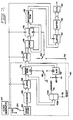
- Fig. 1 shows a block diagram for explaining a first embodiment of the present invention.
- Digital sweep generator 20 provides a sequential digital output signal representing a swept frequency sinewave signal, i.e., a signal of sinusoidal form, the frequency of which varies with time.
- the sweep generator 20 will be described in detail hereinafter with reference to Figs. 4 through 8.
- the digital signal from the digital sweep generator 20 is, for example, ten bit parallel data having a frequency of 14.3 MHz and is applied to a system under test (SUT) 22 which may be a D/A converter, a digital processing system having a D/ A converter 24 as an output stage, or an analog processing system having a D/A converter 24 as an input stage.
- SUT system under test
- the digital signal from generator 20 is converted to an analog signal by the SUT 22, is processed in digital form by the SUT 22 and converted to an analog signal by the D/A converter 24, or is converted to an analog signal by D/ A converter 24 and processed in analog form by the SUT 22 depending on which of the three possible forms is taken by the SUT 22, respectively.
- the analog output signal from SUT 22 is applied to a peak-to-peak (P-P) detector/amplifier 26 which detects the P-P amplitude of the SUT output.
- P-P detector/amplifier 26 will be described in detail hereinafter by reference to Figs. 10 through 15.
- the output level from P-P detector/ amplifier 26 includes envelope gain correction factors, and is applied to the vertical deflection input of an oscilloscope 28.
- the horizontal position of the oscilloscope beam is time dependent, and the horizontal sweep frequency of the oscilloscope is equal to the repetition frequency of the swept frequency sinewave signal. Since the frequency of the sinewave signal provided by the digital sweep generator 20 varies with time, the displayed waveform represents the frequency response of the SUT 22. Thus, the frequency domain characteristic of SUT 22 can be measured without use of an analog-to-digital converter, and the use of the digital test signal provides an accurate evaluation of SUT 22.
- Figs. 2 and 3 show block diagrams for explaining second and third embodiments of the present invention. These embodiments are similar to Fig. 1, so that the same reference numbers have been employed to designate like parts and only the differences will be discussed.
- a high quality standard D/A converter 30 converts the digital signal from the digital sweep generator 20 to a swept frequency sinewave analog signal, and this analog signal is applied to an analog SUT 32.
- the processed analog signal from the SUT 32 is applied to the P-P detector/ amplifier 26 to derive the frequency domain characteristic information of the SUT 32.
- the digital sweep generator 20 generates a marker signal (on line 34) .coincident in time with a specific frequency of the swept frequency sinewave analog signal.
- the marker signal may be displayed by the oscilloscope 28 simultaneously with the output from the P-P detector/ampilfier 26, as shown in Fig. 2, in which the waveform 35 of the marker signal is shown on the oscilloscope 28 with the trace 29 representing the output of the detector/amplifier 26.
- the individual markers may occur at, e.g., 1 MHz intervals. Since an analog circuit is not used for generating the swept frequency sinewave signal, the signal is high quality.
- the D/A converter 30 can be tested using the Fig. 1 circuit with the D/A converter connected as the SUT 22.
- a differential mode employing the present technique may be employed to substantially eliminate the frequency response errors of the test signal.
- An additional P-P detector/amplifier 36, which has the same characteristic as the block 26, and a differential amplifier 38 are added to the Fig. 2 circuit to produce the Fig. 3 circuit.
- the gain of SUT 32 is exactly one, errors in the frequency response of the test signal generator are cancelled by the common mode rejection of differential amplifier 38. It should be noted that the outputs from P-P detectors/amplfiers 26 and 36 are low frequency or d.c.
- the output voltage V from the differential amplifier at any one frequency is given by: where V is the output voltage from the D/A converter at that frequency and A v is the gain of the SUT 32 at that frequency. If the digital sweep generator 20 has a 0.5% frequency response error and the SUT 32 has a 2.0% error, the detected difference (ideally 2.0%) will actually be: In this example, the 0.5% digital sweep generator error resulted in a measurement error of 2.0%-1.99%, namely only 0.01%. Thus, the frequency response error of the test signal is substantially cancelled.
- Fig. 4 shows a basic block diagram of the digital sweep generator 20.
- the digital sweep generator 20 includes a digital data generator 40 which may be a counter, a memory or a thumb wheel switch. Digital data provided by the generator 40 is latched by a latch 42.
- a digital adder 44 such as type 74LS283 IC, adds the digital output data from the latch 42 and a second latch 46, and the result digital data from adder 44 is latched by the latch 46.
- the output data from the latch 46 is applied to the address terminais of a waveform memory 48 which stores digital data representing a cosine waveform, i.e., the memory 48 stores the cosine lookup table.
- the memory 48 may be a ROM, PROM (programmable ROM) EPROM (erasable PROM) or EEPROM (electrically erasable PROM).
- the data output from the waveform ROM 48, is applied to a buffer 52 through a latch 50.
- the latches 42, 46 and 50 may be ICs of type 74LS162, 74LS374 or 74LS377, and their clock terminals receive a clock signal from a clock generator 54.
- the clock frequency is, for example, 14.3 MHz.
- the reset terminal R of the latch 46 is connected to a positive voltage source+or a terminal 58 via a switch 56.
- the output from the buffer 52 is digital data representing the analog waveform determined by the contents of the ROM 48.
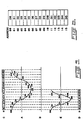
- Fig. 5 shows waveforms for explaining the operation of the sweep generator 20.
- Waveform A is a cosine waveform.
- Waveform B represents the clock pulses provided by the generator 54. Because the clock pulses determine the times at which data is latched by the latch 50, they can be regarded as sampling pulses.
- Cross marks on the waveform A show the sampling points determined by the clock pulses, and DO through D15 represent in digital form (for example 10 bits) the ordinate values of the sampling points.
- the P-P amplitude of the cosinewave A is "11 1111 1111" in the digital data.
- one cycle of the cosinewave A is illustrated as including only sixteen sampling points, but a practical embodiment of the system would include more than sixteen sampling points, for example, 256 sampling points.
- the digital data DO through D15 are stored in the address locations 00 through 15 respectively of the waveform ROM 48, as shown in Fig. 7.
- the digital data generator 40 Assuming that the digital data generator 40 generates continuously the digital data "01” (represented in the decimal code) and the contents of the latch 46 are initially "00”, the data "01” and “00” are latched into the latches 42 and 46, respectively, on the first clock pulse. Simultaneously, the waveform ROM 48 receives the data "00” at its address terminals and generates the data DO (at its data terminals). The adder 44 asynchronously outputs the digitally summed value of the data from the latches 42 and 46, so that the output from the adder 44 is "01" after the first clock pulse.
- the latch 46 stores the data "01” from the adder 44
- the latch 50 stores the data "DO” from the waveform ROM 48.
- the waveform ROM 48 receives the data "01” at its address terminals and generates the data "D1" at its data terminals, and the adder 44 generates the data "02". It should be noted that the contents of the latch 42 do not change because the digital data generator 40 generates the constant value "01".
- the latches 46 and 50 latch the data "02" and "D1" respectively.
- the adder . 44 and waveform ROM 48 generate the data "03" and "D2" respectively. The above-described operation repeats to generate the sequential digital data.
- the adder 44 When the contents of the latch 46 are "15", the adder 44 generates the data "00" and thus returns to its initial condition.
- the data train derived from the buffer 52 is shown in Fig. 5C, and the corresponding analog waveform is shown in Fig. 5A.
- the frequency and amplitude of the analog waveform depend on the clock frequency and the reference voltage of the D/A converter.
- the latch 42 stores the data "02" on the first clock pulse.
- the adder 44 and waveform ROM 48 generate the data "02" and "DO".
- the latches 44 and 50 latch the data "02" and "DO", respectively.
- the adder 44 and waveform ROM 48 generate the data "04" and "D2", and so on.
- the data train from buffer 52 and the corresponding analog waveform from the D/A converter are shown in Figs. 5D and E. If digital data generator 40 generates the data "03”, the data train from buffer 52 is "D0, D3, D6, D9, D12, D15, D2, D5 --. It will be appreciated that the adder 44 and the latches 42 and 46 act as an address generator for the ROM 48.
- the frequency of the digital data from the buffer 52 is constant and is determined only by the clock frequency.
- the frequency of the corresponding analog waveform is determined by both the clock frequency and the setting of the digital data generator 40.
- the digital sweep generator 20 shown in Fig. 4 is implemented using digital circuits only, the digital data from the buffer 52 has a high accuracy, and the analog waveform accuracy depends only on the D/A converter 30.
- phase of the signal output by the D/A converter 30 is reset to a predetermined value, e.g. 0°, at desired times.
- a predetermined value e.g. 0°
- the phase of the test signal should be predictable on every field. Further utility is derived in use of phase measuring systems to reset phase at specific intervals. Reset would not normally be used in conjunction with the detector/amplifier 26 since the sweep signal has greater spectral purity when reset is not employed.
- a swept frequency analog waveform can be derived by varying the output data from the digital data generator 40 and converting the digital data provided by the buffer 52 to analog form.
- Fig. 7 shows a detailed block diagram of the digital sweep generator 20, particularly the digital data generator 40.
- a count down circuit 60 is selectively connected to the clock generator 54 or an external clock terminal 62 via a switch 60.
- the output from the count down circuit 20 is counted by a counter 66 to provide address data which is applied to a latch 68.
- the latch 68 receives a clock pulse, and the output therefrom is applied to the address terminals of a sweep memory 70 and marker/reset circuit 72A, 72B.
- the memory 70 may be a ROM, PROM, EPROM or EEPROM, and it stores information of the sweep rate and linearity.
- the marker/reset circuit 72A, 72B generates the frequency marker and reset signals at terminals 74 and 76 in accordance with the data from the latch 68.
- An A/D converter 78 converts an analog voltage from a potentiometer 80 to digital data.
- the output from the sweep ROM 70 or the A/D converter 78 is applied to the latch 42.
- a switch 82 selectively grounds the chip select terminal CS of the sweep ROM 70 and the enable terminal EN of the A/D converter 78.
- the components 60 through 82 of Fig. 7 form digital data generator 40 of Fig. 5.
- the switch 82 selects the A/D converter 78
- the sweep ROM 70 is disabled and the A/D converter 78 is enabled.
- the latch 42 receives data only from the A/D converter 78, and the frequency of the analog waveform corresponding to the digital output of the buffer 52 can be controlled by the setting of the potentiometer 80. This constitutes a manual control mode of operation.
- the A/D converter 78 When the switch 82 selects the sweep ROM 70, the A/D converter 78 is disabled and the latch 42 receives the data only from the sweep ROM 70. If the contents of the sweep ROM 70 are linear sweep information, a linearly swept frequency sine waveform is derived from the D/A converter 30 as shown in Fig. 8.
- the waveform B is the output from the count down circuit 60 and the counter 66 counts the pulses of the waveform B in order to generate the address data shown by D.
- the address data D is latched into latch 68 on each clock pulse occurrence, and the addresses sweep the ROM 70. When the address data D is "00" at time to, the sweep ROM 70 generates the data "01" for providing digital data from the buffer 52 corresponding to a low frequency sinewave.
- Fig. 8A shows the contents of the sweep ROM 70, i.e., the output data provided by the sweep ROM 70 in the intervals between clock pulses. It will be appreciated that the frequency of the sine waveform does not in fact change linearly-with time, but changes in step-fashion. However, the increments are of equal size and each frequency value is maintained for the same period, and therefore the change in frequency approximates a linear function with respect to time.
- the output from the buffer 52 corresponds to a nonlinearly swept frequency sinewave as shown in Fig. 9C.
- the switch 64 selects the terminal 62, the frequency changing time can be synchronized with an external signal provide at the terminal 62.
- count down circuit 60 may be eliminated and the external signal directly applied to the counter 66 if the frequency of the external signal is much lower than that of the clock pulses from the clock generator 54.
- the marker circuit 72A detects specific addresses provided to the sweep ROM 70 from the latch 68 and generates, at the terminal 74, a marker signal including individual markers which occur when the digital data from the buffer 52 corresponds to selected frequencies of the analog waveform.
- the reset circuit 72B detects the desired intervals of the address data from the counter 66, and generates a reset signal at the terminal 76.
- the reset signal may be applied to the latch 46 via the switch 58 to select output waveforms which are phase-reset at, for example, the horizontal TV scanning interval.
- the latches 40, 46, 50 and 68 receive the clock signals in order to avoid errors due to propagation delay in each block.
- the contents of the ROMs 48 and 70 may be changed. If the sweep rate end linearity are as shown in Fig. 8, the output from converter 66 may be directly applied to latch 42.
- Fig. 10 is a block diagram of the P-P detector/ amplifier 26.
- the P-P detector/amplifier 36 is of like construction.
- the analog signal from the SUT is applied through a terminal 90 to a P-P detector 92 which is of conventional type as shown in Fig. 11.
- Fig. 11 shows an input resistor 94 connected between the input terminal 90 and ground.
- a series circuit consisting of a small resistor 98, a capacitor 100, a diode 102, and an output resistor 104 is inserted between the input terminal 90 and an output terminal 106.
- the junction between the capacitor 100 and the diode 102 is grounded via a diode 108, and the junction between the diode 102 and the resistor 104 is grounded via a capacitor 110.
- Protection Zener diodes 112 and 114 are connected in parallel with the capacitor 110.
- the output from P-P detector 92 is applied to the non-inverting terminal of an input amplifier 116 having its inverting terminal receiving the output from an offset amplifier 118.
- the inverting and non-inverting terminals of the amplifier 118 are respectively connected to a potentiometer 120 and a potentiometer 122 which act as a small signal offset controller and a large signal offset controller, respectively.
- a potentiometer 124 acting as a level controller applies a d.c. voltage to the junction of the potentiometer 122 and a potentiometer 128 through a buffer amplifier 126.
- the potentiometer 128 acts as a large signal gain controller.
- a variable gain amplifier 130 includes a differential amplifier 132 which receives the voltage from the center tap of the potentiometer 128 and also receives the voltage from the centertap of a potentiometer 134 acting as a small signal gain controller.
- the amplifier 130 further includes a multiplier 136 which multiplies the output from input amplifier 116 by the output from the differential amplifier 132 for controlling the output amplitude.
- the push-pull output from the variable gain amplifier 130 is applied to an output terminal 140 through an output amplifier 138.
- a level indicator 142 indicates the output level from the input amplifier 116.
- the amplifier section of P-P detector/amplifier 26 consists of the amplifiers 116, 118, 126, 130 and 138.
- the output from the P-P detector 92 is a d.c. output voltage V out which follows the envelope of the a.c. input signal V in at the terminal 90.
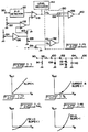
- the output d.c. level from the P-P detector 92 has a gain error that is a function of the signal level as shown in Fig. 13.
- the dynamic gain errors and the d.c. offset are corrected by the amplifier section 130. Since the output from the P-P detector92 changes only a small amount from its nominal d.c. level, it is enough that the gain error is corrected using a first-order approximation at the desired nominal operating point, represented by a circle on the V OUT -V IN characteristic.
- the potentiometer 124 is adjusted to bring the V OUT -V IN characteristic to the desired level, i.e. with the output voltage of the amplifier 140 at the nominal operating point equal to zero, as shown in Fig. 14.
- the level detector 142 indicates the d.c. level of the peak of the envelope signal.
- the potentiometer 124 is used to adjust the level of the output signal of the amplifier 116, through the elements 118, 120, 122, 126, to the desired level.
- the adjustment of the potentiometer 124 controls the gain of the multiplier 136 via the amplifier 132.
- the controllers 120, 122, 128 and 134 are previously calibrated to proper values. Since the voltage from the level controller 124 is zero for small signals, the large signal offset controller 122 has no effect for small signals. Therefore, if the small signal offset controller 120 is adjusted before the large signal offset controller 122 is adjusted, no further interactive adjustment is necessary. Since the V in -V out characteristic of the P-P detector 92 is curved and the slope is less than one as shown in Fig. 13, the curve is offset by the level controller 124 to bring the operating point of interest (illustrated by circles in Figs. 13,14 and 15) back to zero volt d.c. as shown in Fig. 14.
- the P-P detector amplifier/detector 26 (36) is intended for relative frequency response measurements (not absolute amplitude measurement). Then the same setting of the level controller 124 is used to tell the variable gain amplifier 130 what gain correction to apply to tilt the curve back to a 1:1 slope at the desired operating point as shown in Fig. 15. Thus, the gain error correction is completed at the operating point. Since the level indicator 142 includes a window comparator which detects a small level range having zero volt, it is easy to adjust the level controller 124. The frequency domain characteristic of the SUT can be measured accurately by use of P-P detector/ amplifier 26 (36) as well as digital sweep generator 20.
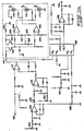
- Fig. 16 shows a detailed circuit diagram of the amplifier section of the P-P detector/amplifier 26.
- the amplifiers 116, 118, 126 and 138 may be type LM308 IC and the variable gain amplifier (mutli- plier) 130 may be type MC1495 IC.
- the output from the input amplifier 116 is applied via a diode connected transistor 152 to the non-inverting input terminals of an upper limit level comparator 154 and a lower limit level comparator 156 which may be type 1458 IC.
- the inverting input terminals of the comparators 154 and 156 respectively receive the upper and lower limit levels from a voltage divider consisting of resistors 158 through 168 and a diode connected transistor 170.
- the transistors 152 and 170 compensate for temperature variation.
- the outputs from the comparators 154 and 156 are “High” and “Low” respectively, causing a red LED 172 to emit light.
- the outputs from the comparators 154 and 156 are both “Low”, causing a red LED 176 to emit light.
- the outputs from the comparators 154 and 156 are respectively “Low” and “High”, causing a green LED 174 to emit light. Therefore, the operator can adjust the level controller 124 to the proper value by observing the LEDs 172, 174 and 176.
- the present invention can provide accurate evaluation of the frequency domain characteristics of the SUT such as a digital processing equipment, a D/A converter and analog processing equipment.
- the output from the P-P detector/amplifier 26 or the differential amplifier 38 may be applied to a digital volt meter instead of an oscilloscope.
- the swept frequency analog signal should be a sinusoidal signal. If a swept frequency analog signal other than a sinusoidal signal were employed, the appropriate waveform would be stored in the lookup table of the memory 48.
- the d.c. level of the peak of the envelope signal could be detected automatically by the indicator 142 and used to provide a feedback signal for adjusting the potentiometer 124 to bring the peak level to the desired level.
Description
- This invention relates to a circuit and method of compensating for variation in the operating characteristics of a peak-to-peak detector and to a use of said method in a method of measuring a frequency domain characteristic of a system under test such as a digital-to-analog converter, a digital processing equipment or an analog processing equipment.
- Use of digital techniques is popular in the field of electronics with the development of microprocessors, and the digital technique is used in analog equipments. A digital-to-analog (D/A) converter is employed to process a digital signal in the analog equipment. It is necessary to measure electronic characteristics of the equipment for insuring the performance thereof. One of the important electrical characteristics is a frequency domain (frequency and phase) response. A swept frequency sinewave test signal is useful for measuring the frequency domain characteristic of the analog equipments. However, since this test signal is analog, it cannot be applied to the digital equipments. The frequency response of the D/A converter may be measured by varying the clock frequency thereto, but the sin x/x correction will not hold constant with frequency variations of the clock.
- Toute L'Electronique No. 451 February 1980, pages 37-40 generally discloses the frequency response testing of a filter using a digitally generated sine function and detecting the envelope of the output signal from the filter for display. FR-A-2,289,915 discloses a peak-to-peak detector having an input terminal to which an input signal is applied, an outputterminal from which an output signal is obtained and the input and output terminals defining a signal path in which is located a first diode. A second diode is coupled between the input terminal and a reference voltage level. The detector disclosed in the French Patent suffers from the disadvantage that the operating characteristic is non-linear and it is an object of this invention to provide a circuit and method for compensating the operating characteristic variation.
- According to a first aspect of the-present invention there is provided peak-to-peak detection apparatus comprising a peak-to-peak detector having an input terminal, an output terminal, the input and output terminals defining a signal path therebetween, a first diode coupled in said signal path between the input and output terminals, and a second diode coupled between the signal path and a reference potential level, whereby the detector is arranged to generate at its output terminal an output signal representing the envelope of an input signal applied to its input terminal, characterised in that there is provided means for compensating for the effect of the operating characteristic of the detector of the change in incremental dynamic impedance of the diodes with input signal level, the compensating means comprising means for determining the level of the output signal of the detector at a predetermined point of the output-input characteristic of the detector corresponding to a nominal input signal level, means for adjusting the d.c. level of said detector output signal to bring it at said predetermined point to a desired level, and amplifying means for amplifying the adjusted output signal by an amount dependent upon the adjustment made to the d.c. level of thetdetector output signal, the output of the amplifying means corresponding to the output of the said apparatus.
- According to a second aspect of this invention there is provided a method of detecting a peak-to-peak signal with a peak-to-peak detector having an input terminal and an output terminal, the input and output terminals defining a signal path therebetween, a first diode coupled in said signal path between the input and output terminals, and a second diode coupled between the signal path and a reference potential level, said detector being arranged to generate at its output terminal an output signal representing the envelope of an input signal applied to the input terminal thereof, said method being characterised by the steps of:
- compensating for the effect of the operating characteristic of the detector of the change in incremental dynamic impedance of the diodes with input signal level, said compensating step including determining the level of the output signal of the detector at a predetermined point of the output-input characteristic of the detector corresponding to a nominal input signal level adjusting the d.c. level of said detector output signal to bring it at said predetermined point to a desired level and amplifying the adjusted output signal by an amount dependent upon the adjustment made to the d.c. level of the detector output signal.
- Various uses of the method are defined in
claims - For a better understanding of the invention, and to show how the same may be carried into effect, reference will now be made, by way of example, to the accompanying drawings in which:
- Figures 1, 2 and 3 are block diagrams of respective apparatus for measuring a frequency domain characteristic;
- Figure 4 is a block diagram of a sweep generator part of the apparatus;
- Figures 5 and 6 are respectively, graphs and a table for illustrating the operation of Figure 4;
- Figure 7 is a block diagram showing a digital data generator of Figure 4 in greater detail;
- Figures 8 and 9 are graphs illustrating the operation of Figure 7;
- Figure 10 illustrates, partly in block form and partly in schematic form, a peak-to-peak detector/ amplifier used in the apparatus of Figures 1 to 3 and which is in accordance with this invention;
- Figure 11 is a schematic diagram of one component of Figure 10;
- Figures 12-15 are graphs illustrating operation of Figure 10; and
- Figure 16 is a circuit diagram of the ampifier section o1 Figure 10.
- Fig. 1 shows a block diagram for explaining a first embodiment of the present invention.
Digital sweep generator 20 provides a sequential digital output signal representing a swept frequency sinewave signal, i.e., a signal of sinusoidal form, the frequency of which varies with time. Thesweep generator 20 will be described in detail hereinafter with reference to Figs. 4 through 8. The digital signal from thedigital sweep generator 20 is, for example, ten bit parallel data having a frequency of 14.3 MHz and is applied to a system under test (SUT) 22 which may be a D/A converter, a digital processing system having a D/A converter 24 as an output stage, or an analog processing system having a D/A converter 24 as an input stage. The digital signal fromgenerator 20 is converted to an analog signal by theSUT 22, is processed in digital form by theSUT 22 and converted to an analog signal by the D/A converter 24, or is converted to an analog signal by D/A converter 24 and processed in analog form by theSUT 22 depending on which of the three possible forms is taken by theSUT 22, respectively. The analog output signal from SUT 22 is applied to a peak-to-peak (P-P) detector/amplifier 26 which detects the P-P amplitude of the SUT output. P-P detector/amplifier 26 will be described in detail hereinafter by reference to Figs. 10 through 15. The output level from P-P detector/amplifier 26 includes envelope gain correction factors, and is applied to the vertical deflection input of anoscilloscope 28. The horizontal position of the oscilloscope beam is time dependent, and the horizontal sweep frequency of the oscilloscope is equal to the repetition frequency of the swept frequency sinewave signal. Since the frequency of the sinewave signal provided by thedigital sweep generator 20 varies with time, the displayed waveform represents the frequency response of theSUT 22. Thus, the frequency domain characteristic of SUT 22 can be measured without use of an analog-to-digital converter, and the use of the digital test signal provides an accurate evaluation ofSUT 22. - Figs. 2 and 3 show block diagrams for explaining second and third embodiments of the present invention. These embodiments are similar to Fig. 1, so that the same reference numbers have been employed to designate like parts and only the differences will be discussed. In Fig. 2, a high quality standard D/
A converter 30 converts the digital signal from thedigital sweep generator 20 to a swept frequency sinewave analog signal, and this analog signal is applied to ananalog SUT 32. The processed analog signal from the SUT 32 is applied to the P-P detector/amplifier 26 to derive the frequency domain characteristic information of theSUT 32. In this embodiment, thedigital sweep generator 20 generates a marker signal (on line 34) .coincident in time with a specific frequency of the swept frequency sinewave analog signal. The marker signal may be displayed by theoscilloscope 28 simultaneously with the output from the P-P detector/ampilfier 26, as shown in Fig. 2, in which thewaveform 35 of the marker signal is shown on theoscilloscope 28 with thetrace 29 representing the output of the detector/amplifier 26. The individual markers may occur at, e.g., 1 MHz intervals. Since an analog circuit is not used for generating the swept frequency sinewave signal, the signal is high quality. The D/A converter 30 can be tested using the Fig. 1 circuit with the D/A converter connected as theSUT 22. - When the frequency response errors of the test signal source (
digital sweep generator 20 and D/A converter 30) are significant compared to the expected errors ofSUT 32, a differential mode employing the present technique may be employed to substantially eliminate the frequency response errors of the test signal. An additional P-P detector/amplifier 36, which has the same characteristic as theblock 26, and adifferential amplifier 38 are added to the Fig. 2 circuit to produce the Fig. 3 circuit. When the gain of SUT 32 is exactly one, errors in the frequency response of the test signal generator are cancelled by the common mode rejection ofdifferential amplifier 38. It should be noted that the outputs from P-P detectors/amplfiers differential amplifier 38 does not affect the measurement of the frequency domain characteristics of theSUT 32. The output voltage V from the differential amplifier at any one frequency is given by:
SUT 32 at that frequency. If thedigital sweep generator 20 has a 0.5% frequency response error and the SUT 32 has a 2.0% error, the detected difference (ideally 2.0%) will actually be:
- Fig. 4 shows a basic block diagram of the
digital sweep generator 20. Thedigital sweep generator 20 includes adigital data generator 40 which may be a counter, a memory or a thumb wheel switch. Digital data provided by thegenerator 40 is latched by alatch 42. Adigital adder 44, such as type 74LS283 IC, adds the digital output data from thelatch 42 and asecond latch 46, and the result digital data fromadder 44 is latched by thelatch 46. The output data from thelatch 46 is applied to the address terminais of awaveform memory 48 which stores digital data representing a cosine waveform, i.e., thememory 48 stores the cosine lookup table. Thememory 48 may be a ROM, PROM (programmable ROM) EPROM (erasable PROM) or EEPROM (electrically erasable PROM). The data output from thewaveform ROM 48, is applied to abuffer 52 through alatch 50. Thelatches clock generator 54. The clock frequency is, for example, 14.3 MHz. The reset terminal R of thelatch 46 is connected to a positive voltage source+or a terminal 58 via aswitch 56. The output from thebuffer 52 is digital data representing the analog waveform determined by the contents of theROM 48. - Fig. 5 shows waveforms for explaining the operation of the
sweep generator 20. Waveform A is a cosine waveform. Waveform B represents the clock pulses provided by thegenerator 54. Because the clock pulses determine the times at which data is latched by thelatch 50, they can be regarded as sampling pulses. Cross marks on the waveform A show the sampling points determined by the clock pulses, and DO through D15 represent in digital form (for example 10 bits) the ordinate values of the sampling points. The P-P amplitude of the cosinewave A is "11 1111 1111" in the digital data. In order to simplify the description, one cycle of the cosinewave A is illustrated as including only sixteen sampling points, but a practical embodiment of the system would include more than sixteen sampling points, for example, 256 sampling points. The digital data DO through D15 are stored in theaddress locations 00 through 15 respectively of thewaveform ROM 48, as shown in Fig. 7. - Assuming that the
digital data generator 40 generates continuously the digital data "01" (represented in the decimal code) and the contents of thelatch 46 are initially "00", the data "01" and "00" are latched into thelatches waveform ROM 48 receives the data "00" at its address terminals and generates the data DO (at its data terminals). Theadder 44 asynchronously outputs the digitally summed value of the data from thelatches adder 44 is "01" after the first clock pulse. When the second clock pulse occurs, thelatch 46 stores the data "01" from theadder 44, and thelatch 50 stores the data "DO" from thewaveform ROM 48. After the second clock pulse, thewaveform ROM 48 receives the data "01" at its address terminals and generates the data "D1" at its data terminals, and theadder 44 generates the data "02". It should be noted that the contents of thelatch 42 do not change because thedigital data generator 40 generates the constant value "01". When the third clock pulse occurs, thelatches waveform ROM 48 generate the data "03" and "D2" respectively. The above-described operation repeats to generate the sequential digital data. When the contents of thelatch 46 are "15", theadder 44 generates the data "00" and thus returns to its initial condition. The data train derived from thebuffer 52 is shown in Fig. 5C, and the corresponding analog waveform is shown in Fig. 5A. The frequency and amplitude of the analog waveform depend on the clock frequency and the reference voltage of the D/A converter. - If the output from the
digital data generator 40 is continuously "02", thelatch 42 stores the data "02" on the first clock pulse. Theadder 44 andwaveform ROM 48 generate the data "02" and "DO". When the second clock pulse occurs, thelatches adder 44 andwaveform ROM 48 generate the data "04" and "D2", and so on. The data train frombuffer 52 and the corresponding analog waveform from the D/A converter are shown in Figs. 5D and E. Ifdigital data generator 40 generates the data "03", the data train frombuffer 52 is "D0, D3, D6, D9, D12, D15, D2, D5...". It will be appreciated that theadder 44 and thelatches ROM 48. - As will be understood from the foregoing description, the frequency of the digital data from the
buffer 52 is constant and is determined only by the clock frequency. However, the frequency of the corresponding analog waveform is determined by both the clock frequency and the setting of thedigital data generator 40. Thus, it is not necessary to change the clock frequency of the D/A converter 30 in order to change the analog waveform frequency, so that the SUT does not need to change the electrical characteristics associated with the clock frequency, such as sin x/x correction. Since thedigital sweep generator 20 shown in Fig. 4 is implemented using digital circuits only, the digital data from thebuffer 52 has a high accuracy, and the analog waveform accuracy depends only on the D/A converter 30. Ifswitch 56 selects terminal 58, which receives a sync signal, latch 46 is reset to provide an output "00" at every occurrence of the sync signal, so that the digital data frombuffer 52 is synchronized with the sync signal. This allows the phase of the signal output by the D/A converter 30 to be reset to a predetermined value, e.g. 0°, at desired times. For example, in the evaluation of picture monitor displays, the phase of the test signal should be predictable on every field. Further utility is derived in use of phase measuring systems to reset phase at specific intervals. Reset would not normally be used in conjunction with the detector/amplifier 26 since the sweep signal has greater spectral purity when reset is not employed. A swept frequency analog waveform can be derived by varying the output data from thedigital data generator 40 and converting the digital data provided by thebuffer 52 to analog form. - Fig. 7 shows a detailed block diagram of the
digital sweep generator 20, particularly thedigital data generator 40. A count downcircuit 60 is selectively connected to theclock generator 54 or an external clock terminal 62 via aswitch 60. The output from the count downcircuit 20 is counted by acounter 66 to provide address data which is applied to alatch 68. Thelatch 68 receives a clock pulse, and the output therefrom is applied to the address terminals of asweep memory 70 and marker/reset circuit memory 70 may be a ROM, PROM, EPROM or EEPROM, and it stores information of the sweep rate and linearity. The marker/reset circuit terminals latch 68. An A/D converter 78 converts an analog voltage from apotentiometer 80 to digital data. The output from thesweep ROM 70 or the A/D converter 78 is applied to thelatch 42. Aswitch 82 selectively grounds the chip select terminal CS of thesweep ROM 70 and the enable terminal EN of the A/D converter 78. Thecomponents 60 through 82 of Fig. 7 formdigital data generator 40 of Fig. 5. - When the
switch 82 selects the A/D converter 78, thesweep ROM 70 is disabled and the A/D converter 78 is enabled. In this instance, thelatch 42 receives data only from the A/D converter 78, and the frequency of the analog waveform corresponding to the digital output of thebuffer 52 can be controlled by the setting of thepotentiometer 80. This constitutes a manual control mode of operation. - When the
switch 82 selects thesweep ROM 70, the A/D converter 78 is disabled and thelatch 42 receives the data only from thesweep ROM 70. If the contents of thesweep ROM 70 are linear sweep information, a linearly swept frequency sine waveform is derived from the D/A converter 30 as shown in Fig. 8. The waveform B is the output from the count downcircuit 60 and the counter 66 counts the pulses of the waveform B in order to generate the address data shown by D. The address data D is latched intolatch 68 on each clock pulse occurrence, and the addresses sweep theROM 70. When the address data D is "00" at time to, thesweep ROM 70 generates the data "01" for providing digital data from thebuffer 52 corresponding to a low frequency sinewave. When the data D becomes "01" at the t1, the data from thesweep ROM 70 is "02" and the sinewave frequency is increased. These operations are repeated, whereby the digital data corresponding to the swept frequency sinewave shown in Fig. 8C is derived from thebuffer 52. Fig. 8A shows the contents of thesweep ROM 70, i.e., the output data provided by thesweep ROM 70 in the intervals between clock pulses. It will be appreciated that the frequency of the sine waveform does not in fact change linearly-with time, but changes in step-fashion. However, the increments are of equal size and each frequency value is maintained for the same period, and therefore the change in frequency approximates a linear function with respect to time. - If the sweep rate and linearity information in the
ROM 70 is not linear as shown in Fig. 9A, the output from thebuffer 52 corresponds to a nonlinearly swept frequency sinewave as shown in Fig. 9C. When theswitch 64 selects the terminal 62, the frequency changing time can be synchronized with an external signal provide at the terminal 62. In this instance, count downcircuit 60 may be eliminated and the external signal directly applied to thecounter 66 if the frequency of the external signal is much lower than that of the clock pulses from theclock generator 54. - The
marker circuit 72A detects specific addresses provided to thesweep ROM 70 from thelatch 68 and generates, at the terminal 74, a marker signal including individual markers which occur when the digital data from thebuffer 52 corresponds to selected frequencies of the analog waveform. Thereset circuit 72B detects the desired intervals of the address data from thecounter 66, and generates a reset signal at the terminal 76. The reset signal may be applied to thelatch 46 via theswitch 58 to select output waveforms which are phase-reset at, for example, the horizontal TV scanning interval. - The
latches ROMs converter 66 may be directly applied to latch 42. - Fig. 10 is a block diagram of the P-P detector/
amplifier 26. The P-P detector/amplifier 36 is of like construction. The analog signal from the SUT is applied through a terminal 90 to aP-P detector 92 which is of conventional type as shown in Fig. 11. Fig. 11 shows aninput resistor 94 connected between the input terminal 90 and ground. A series circuit consisting of a small resistor 98, a capacitor 100, a diode 102, and anoutput resistor 104 is inserted between the input terminal 90 and anoutput terminal 106. The junction between the capacitor 100 and the diode 102 is grounded via adiode 108, and the junction between the diode 102 and theresistor 104 is grounded via acapacitor 110. Protection Zener diodes 112 and 114 are connected in parallel with thecapacitor 110. - Returning to Fig. 10, the output from
P-P detector 92 is applied to the non-inverting terminal of aninput amplifier 116 having its inverting terminal receiving the output from an offsetamplifier 118. The inverting and non-inverting terminals of theamplifier 118 are respectively connected to apotentiometer 120 and apotentiometer 122 which act as a small signal offset controller and a large signal offset controller, respectively. Apotentiometer 124 acting as a level controller applies a d.c. voltage to the junction of thepotentiometer 122 and apotentiometer 128 through abuffer amplifier 126. Thepotentiometer 128 acts as a large signal gain controller. Avariable gain amplifier 130 includes adifferential amplifier 132 which receives the voltage from the center tap of thepotentiometer 128 and also receives the voltage from the centertap of apotentiometer 134 acting as a small signal gain controller. Theamplifier 130 further includes amultiplier 136 which multiplies the output frominput amplifier 116 by the output from thedifferential amplifier 132 for controlling the output amplitude. The push-pull output from thevariable gain amplifier 130 is applied to anoutput terminal 140 through anoutput amplifier 138. Alevel indicator 142 indicates the output level from theinput amplifier 116. The amplifier section of P-P detector/amplifier 26 consists of theamplifiers - The output from the
P-P detector 92 is a d.c. output voltage Vout which follows the envelope of the a.c. input signal Vin at the terminal 90. An ideal detectorwould have Vout/Vin=1 as shown in Fig. 12. However, due to the turn on voltages and dynamic impedances of thediodes 102 and 108 in theP-P detector 92, the output d.c. level from theP-P detector 92 has a gain error that is a function of the signal level as shown in Fig. 13. The dynamic gain errors and the d.c. offset are corrected by theamplifier section 130. Since the output from the P-P detector92 changes only a small amount from its nominal d.c. level, it is enough that the gain error is corrected using a first-order approximation at the desired nominal operating point, represented by a circle on the VOUT-VIN characteristic. - The
potentiometer 124 is adjusted to bring the VOUT-VIN characteristic to the desired level, i.e. with the output voltage of theamplifier 140 at the nominal operating point equal to zero, as shown in Fig. 14. Thelevel detector 142 indicates the d.c. level of the peak of the envelope signal. Thepotentiometer 124 is used to adjust the level of the output signal of theamplifier 116, through theelements potentiometer 124 controls the gain of themultiplier 136 via theamplifier 132. - In order to correct the gain error of the
P-P detector 92, thecontrollers level controller 124 is zero for small signals, the large signal offsetcontroller 122 has no effect for small signals. Therefore, if the small signal offsetcontroller 120 is adjusted before the large signal offsetcontroller 122 is adjusted, no further interactive adjustment is necessary. Since the Vin-Vout characteristic of theP-P detector 92 is curved and the slope is less than one as shown in Fig. 13, the curve is offset by thelevel controller 124 to bring the operating point of interest (illustrated by circles in Figs. 13,14 and 15) back to zero volt d.c. as shown in Fig. 14. It should be noted that the P-P detector amplifier/detector 26 (36) is intended for relative frequency response measurements (not absolute amplitude measurement). Then the same setting of thelevel controller 124 is used to tell thevariable gain amplifier 130 what gain correction to apply to tilt the curve back to a 1:1 slope at the desired operating point as shown in Fig. 15. Thus, the gain error correction is completed at the operating point. Since thelevel indicator 142 includes a window comparator which detects a small level range having zero volt, it is easy to adjust thelevel controller 124. The frequency domain characteristic of the SUT can be measured accurately by use of P-P detector/ amplifier 26 (36) as well asdigital sweep generator 20. - Fig. 16 shows a detailed circuit diagram of the amplifier section of the P-P detector/
amplifier 26. Theamplifiers input amplifier 116 is applied via a diode connectedtransistor 152 to the non-inverting input terminals of an upperlimit level comparator 154 and a lowerlimit level comparator 156 which may be type 1458 IC. The inverting input terminals of thecomparators resistors 158 through 168 and a diode connectedtransistor 170. Thetransistors input amplifier 116 is higher than the upper limit level, the outputs from thecomparators red LED 172 to emit light. When the output level from theinput amplifier 116 is lower than the lower limit level, the outputs from thecomparators red LED 176 to emit light. When the output level from theinput amplifier 116 is between the lower and upper limit levels, the outputs from thecomparators green LED 174 to emit light. Therefore, the operator can adjust thelevel controller 124 to the proper value by observing theLEDs - As understood from the foregoing description, the present invention can provide accurate evaluation of the frequency domain characteristics of the SUT such as a digital processing equipment, a D/A converter and analog processing equipment.
- It will be appreciated that the present invention is not restricted to the particular methods and apparatus which have been described with reference to the drawings, and that variations may be made without departing from the scope of the invention as defined in the appended claims, and equivalents thereof. For example, the output from the P-P detector/
amplifier 26 or thedifferential amplifier 38 may be applied to a digital volt meter instead of an oscilloscope. Also, it is not essential to the invention that the swept frequency analog signal should be a sinusoidal signal. If a swept frequency analog signal other than a sinusoidal signal were employed, the appropriate waveform would be stored in the lookup table of thememory 48. Furthermore, instead of providing for operator interaction in setting thepotentiometer 124, the d.c. level of the peak of the envelope signal could be detected automatically by theindicator 142 and used to provide a feedback signal for adjusting thepotentiometer 124 to bring the peak level to the desired level.
Claims (12)
Applications Claiming Priority (2)
| Application Number | Priority Date | Filing Date | Title |
|---|---|---|---|
| JP52164/82 | 1982-03-30 | ||
| JP5216482A JPS58169067A (en) | 1982-03-30 | 1982-03-30 | Method of measuring frequency-region characteristic |
Publications (3)
| Publication Number | Publication Date |
|---|---|
| EP0095234A2 EP0095234A2 (en) | 1983-11-30 |
| EP0095234A3 EP0095234A3 (en) | 1986-03-26 |
| EP0095234B1 true EP0095234B1 (en) | 1990-01-17 |
Family
ID=12907186
Family Applications (1)
| Application Number | Title | Priority Date | Filing Date |
|---|---|---|---|
| EP19830301804 Expired - Lifetime EP0095234B1 (en) | 1982-03-30 | 1983-03-30 | Signal peak-to-peak detection method and apparatus |
Country Status (4)
| Country | Link |
|---|---|
| EP (1) | EP0095234B1 (en) |
| JP (1) | JPS58169067A (en) |
| CA (1) | CA1224845A (en) |
| DE (1) | DE3381119D1 (en) |
Families Citing this family (1)
| Publication number | Priority date | Publication date | Assignee | Title |
|---|---|---|---|---|
| DE102006031027A1 (en) * | 2006-07-05 | 2008-01-24 | Atmel Germany Gmbh | Method for checking the function of at least one analog circuit block |
Family Cites Families (2)
| Publication number | Priority date | Publication date | Assignee | Title |
|---|---|---|---|---|
| US2924769A (en) * | 1958-06-16 | 1960-02-09 | Gen Electric | Peak reading circuit |
| IT1025356B (en) * | 1974-10-31 | 1978-08-10 | Ates Componenti Elettron | CASCADE DETECTOR DUPLICATOR CIRCUIT |
-
1982
- 1982-03-30 JP JP5216482A patent/JPS58169067A/en active Granted
-
1983
- 1983-03-30 DE DE8383301804T patent/DE3381119D1/en not_active Expired - Fee Related
- 1983-03-30 CA CA000424902A patent/CA1224845A/en not_active Expired
- 1983-03-30 EP EP19830301804 patent/EP0095234B1/en not_active Expired - Lifetime
Also Published As
| Publication number | Publication date |
|---|---|
| EP0095234A2 (en) | 1983-11-30 |
| CA1224845A (en) | 1987-07-28 |
| JPS58169067A (en) | 1983-10-05 |
| EP0095234A3 (en) | 1986-03-26 |
| DE3381119D1 (en) | 1990-02-22 |
| JPH0368351B2 (en) | 1991-10-28 |
Similar Documents
| Publication | Publication Date | Title |
|---|---|---|
| US4553091A (en) | Automatic vertical calibration method and system for an oscilloscope | |
| US4799008A (en) | AC level calibration apparatus | |
| US5642300A (en) | Precision voltage/current/power source | |
| US4613814A (en) | Method of measuring a frequency domain characteristic | |
| US4958294A (en) | Swept microwave power measurement system and method | |
| US3934197A (en) | Automatic calibration system | |
| US4628254A (en) | Method for digitally measuring waveforms | |
| EP0321963A1 (en) | Impedance measuring apparatus | |
| US4743845A (en) | Oscilloscope-based signal level measurement system | |
| US4390949A (en) | Electronic system and method for self-calibration of instrument landing systems | |
| US4901078A (en) | Variable duty cycle window detecting analog to digital converter | |
| EP0095234B1 (en) | Signal peak-to-peak detection method and apparatus | |
| US4605868A (en) | Peak-to-peak detection apparatus | |
| US4785419A (en) | Logarithmic amplifier calibrator | |
| CA1151771A (en) | Method and apparatus for enhancing the output of an rms converter | |
| US3500198A (en) | Apparatus and method for measuring the logarithm of the root-mean-square value of a signal | |
| JPH01195371A (en) | Measurer | |
| US5043909A (en) | Method and device for excess modulation detection for signal analysis | |
| US10267932B2 (en) | Method and apparatus for X-ray detection system gain calibration using a pulser | |
| USH1458H (en) | Signal amplitude distribution analyzer | |
| RU2159446C1 (en) | Stroboscopic transducer calibration process | |
| RU1777160C (en) | Device for determining static characteristics of random processes | |
| JPH077015B2 (en) | Automatic calibration device for inclined waveform generator | |
| GB2159965A (en) | Method for the measurement of capacitance | |
| SU351166A1 (en) | NSH BIB.PIOTGKA |
Legal Events
| Date | Code | Title | Description |
|---|---|---|---|
| PUAI | Public reference made under article 153(3) epc to a published international application that has entered the european phase |
Free format text: ORIGINAL CODE: 0009012 |
|
| AK | Designated contracting states |
Designated state(s): DE GB NL |
|
| PUAL | Search report despatched |
Free format text: ORIGINAL CODE: 0009013 |
|
| AK | Designated contracting states |
Kind code of ref document: A3 Designated state(s): DE GB NL |
|
| 17P | Request for examination filed |
Effective date: 19860724 |
|
| 17Q | First examination report despatched |
Effective date: 19880504 |
|
| GRAA | (expected) grant |
Free format text: ORIGINAL CODE: 0009210 |
|
| AK | Designated contracting states |
Kind code of ref document: B1 Designated state(s): DE GB NL |
|
| REF | Corresponds to: |
Ref document number: 3381119 Country of ref document: DE Date of ref document: 19900222 |
|
| PLBE | No opposition filed within time limit |
Free format text: ORIGINAL CODE: 0009261 |
|
| STAA | Information on the status of an ep patent application or granted ep patent |
Free format text: STATUS: NO OPPOSITION FILED WITHIN TIME LIMIT |
|
| 26N | No opposition filed | ||
| PGFP | Annual fee paid to national office [announced via postgrant information from national office to epo] |
Ref country code: NL Payment date: 19920331 Year of fee payment: 10 |
|
| PGFP | Annual fee paid to national office [announced via postgrant information from national office to epo] |
Ref country code: GB Payment date: 19930217 Year of fee payment: 11 |
|
| PGFP | Annual fee paid to national office [announced via postgrant information from national office to epo] |
Ref country code: DE Payment date: 19930222 Year of fee payment: 11 |
|
| PG25 | Lapsed in a contracting state [announced via postgrant information from national office to epo] |
Ref country code: NL Effective date: 19931001 |
|
| NLV4 | Nl: lapsed or anulled due to non-payment of the annual fee | ||
| PG25 | Lapsed in a contracting state [announced via postgrant information from national office to epo] |
Ref country code: GB Effective date: 19940330 |
|
| GBPC | Gb: european patent ceased through non-payment of renewal fee |
Effective date: 19940330 |
|
| PG25 | Lapsed in a contracting state [announced via postgrant information from national office to epo] |
Ref country code: DE Effective date: 19941201 |