EP0095223B1 - A lead frame - Google Patents
A lead frame Download PDFInfo
- Publication number
- EP0095223B1 EP0095223B1 EP83200752A EP83200752A EP0095223B1 EP 0095223 B1 EP0095223 B1 EP 0095223B1 EP 83200752 A EP83200752 A EP 83200752A EP 83200752 A EP83200752 A EP 83200752A EP 0095223 B1 EP0095223 B1 EP 0095223B1
- Authority
- EP
- European Patent Office
- Prior art keywords
- lead
- lands
- leads
- micro
- carrier plate
- Prior art date
- Legal status (The legal status is an assumption and is not a legal conclusion. Google has not performed a legal analysis and makes no representation as to the accuracy of the status listed.)
- Expired
Links
Images
Classifications
-
- H—ELECTRICITY
- H10—SEMICONDUCTOR DEVICES; ELECTRIC SOLID-STATE DEVICES NOT OTHERWISE PROVIDED FOR
- H10W—GENERIC PACKAGES, INTERCONNECTIONS, CONNECTORS OR OTHER CONSTRUCTIONAL DETAILS OF DEVICES COVERED BY CLASS H10
- H10W70/00—Package substrates; Interposers; Redistribution layers [RDL]
- H10W70/40—Leadframes
- H10W70/421—Shapes or dispositions
-
- H—ELECTRICITY
- H10—SEMICONDUCTOR DEVICES; ELECTRIC SOLID-STATE DEVICES NOT OTHERWISE PROVIDED FOR
- H10W—GENERIC PACKAGES, INTERCONNECTIONS, CONNECTORS OR OTHER CONSTRUCTIONAL DETAILS OF DEVICES COVERED BY CLASS H10
- H10W70/00—Package substrates; Interposers; Redistribution layers [RDL]
- H10W70/40—Leadframes
- H10W70/421—Shapes or dispositions
- H10W70/438—Shapes or dispositions of side rails, e.g. having holes
Definitions
- the invention relates to a lead frame for applying micro-electronic elements thereto, as known e.g. from FR-A-2,188,305, said frame comprising a series of lead patterns disposed at identical pitch distances, each consisting of a carrier plate lying on the axis of the frame for applying a micro-electronic element thereto, further of leads terminating a short distance from said carrier plate, said leads being connected to lands extending perpendicularly to the frame axis and disposed on either side of the carrier plate, said leads extending beyond said lands in mutually parallel relationship so as to form lead terminals.
- Such lead frames are generally known stamping products, which . are frequently employed in practice.
- On the carrier plate of each lead pattern there is provided an electronic micro-element, the terminations of which are soldered onto the separate leads of the lead pattern.
- the element together with the soldered connections is encapsulated in a resin envelope, after which the resulting encapsulated micro-electronic element is detached from the lead frame by severing all connections of the encapsulated micro-electronic element to the lead frame.
- the lands on either side of the lead terminals are severed, thereby bending the lead terminals, enabling a convenient mounting of the encapsulated micro-electronic element on printing plates.
- the lands disposed between the leads and the lead terminals have a double function, viz.:
- the required distance between the lands and the side edges of the envelope of the micro-electronic element results in that the spaces lying within said distance (squares) between the lead patterns are filled with resin, which resin, after the encapsulation of the micro-electronic element, has to be removed mechanically.
- the pitch distance between the lead patterns there is also known a lead frame wherein the lead terminals extend up to the next land of the adjoining lead pattern, being connected thereto, while the parallel leads of adjoining patterns are shifted relatively to each other in transverse direction.
- This lead frame is usually defined as an "interdigitated lead frame".
- the pitch distance between the lead patterns can be considerably shortened in that the lead terminals are no longer co-extensive.
- the pitch distance, relative to the above described lead pattern is thus shortened by the length of one lead terminal.
- the mutual distance between the lands on either side of the lead pattern is not affected thereby and there necessarily remains a minimal distance between the edge of the land and the side edge of the envelope of the encapsulated, micro-electronic element.
- the distance between the carrier plate for the micro-electronic element and the edge of the land can be further reduced in that during the severing of the encapsulated element only the land portion farthest removed from the envelope need be severed. Consequently, the land may extend up to the side wall of the envelope. In this manner, a mechanical finishing of the leads or lead terminals projecting from the envelope can be dispensed with.
- the pitch distance can be reduced by a distance approximately corresponding with 2x2/3xthe land width when the cuts are applied over 2/3 part of the land width. This means a reduction of the pitch distance and hence a saving in material of about 8-10%. This saving in material is important, since the cost of manufacture of lead frames consists as to about 70% of material cost.
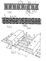
- Figure 1 shows a known and frequently employed lead frame 1, comprising uniformly interspaced lead patterns 2, in the centre of which there is provided a carrier plate 3 for applying a micro-electronic element thereto.
- the lead pattern 2 comprises a plurality of leads 5 terminating a short distance from the carrier plate 3, said leads extending to the lands 6, 7 disposed on either side of the lead pattern 2. Adjacent the lands 6, 7 the leads extend in parallel relationship, being extended for forming the lead terminals 4 associated with two adjoining lead patterns 2.
- the arrow P indicates the pitch distance of the lead frame 1.
- the mutual distance of the lands 6, 7 located on either side of a lead pattern 2 is indicated by arrow 9, while arrow 8 indicates the width of the resin-encapsulated micro-electronic element applied to the carrier plate 3.
- the distance 8 is less than the distance 9 and arrow 10 indicates the distance between the trailing edge of a land 7 and the leading edge of an envelope. Said distance 10 is primarily determined by tolerances and in practice is minimally 0.3 mm. Cutting the lands 6, 7 on either side of the leads 5 or the lead terminals 4 should take place at some distance from the resin envelope, so as to prevent damage thereto.
- each carrier plate 3 of the lead frame 1 there is applied a micro-electronic element, the terminations of which are each connected to one lead 5 of a lead pattern 2 by means of soldering.
- the lead frame is then installed in a cast-in die, comprising two half-dies containing recesses for the envelope of the micro-electronic element.
- the two half-dies abut against those portions of the lead frame 1 that are not to be provided with a resin envelope.
- the lands 6, 7 should ensure such a sealing that the resin space between the lead terminals 4 is not filled up. In doing so, it cannot be avoided that the space between the leads 5 adjacent a land 6, 7 is filled with epoxy resin, as shown in Figure 1 by 11. These epoxy squares 11 are subsequently to be removed mechanically.
- the encapsulated micro-electronic element is to be severed from the lead frame 1, with the lead terminals 4 being severed in the centre, as also are lands 6, 7 on either side of the leads 5 or the lead terminals 4. Naturally, the edges of the lead frame 1 are also removed thereby.
- Figure 2 shows a slightly modified lead frame 20, the pitch distance P 2 of which is substantially reduced relative to the lead frame 1 of Figure 1, viz. by a length corresponding with one lead terminal 24.
- This reduction of the pitch distance P 2 can be obtained by shifting the lead terminals 24 of two adjoining lead patterns 22a-22b in transverse direction, so that they are no longer co-extensive but in side-by-side relationship.
- the mutual distance between the lands 6, 7 is not changed thereby, as indicated by the arrow 29.
- the distance 29 is therefore equal to the distance 9 in Figure 1.
- Figure 3 shows a part of a lead frame having two encapsulated adjoining micro-electronic elements, the envelopes of which are indicated by 40, 41.
- the land 36 At the right hand side of the envelope 40, there is provided the land 36 and at the left hand side of the envelope 41 is indicated the land 37.
- the lead terminals 34, associated with the element 40 extend up to, and are connected to, the land 37 associated with the element 41, while the lead terminals 35 associated with the latter element extend up to, and are connected to, the land 36.
- At 50 is indicated the minimal distance corresponding with the distance 10 in Figure 1, i.e. mechanical cutting operations can only take place at a distance 50 from the side edge of the envelope 40.
- the land 36 extends up to the sidewall of the envelope 40.
- the width 38 of the envelope 40 consequently, is equal to the distance 39 between the lands 36 on either side of the envelope 40.
- Said lands contain a series of cuts 51 terminating a short distance from the edge of the land 36.
- the cuts 51 can be applied in any place situated between two adjoining lead terminals 34, 35, so that the width of the foot 43 of the lead terminal can be varied.
- the cuts 51 are applied in the plane through the sidewalls of the terminals 34, or for the land 37 through the sidewalls of the terminals 35.
Landscapes
- Lead Frames For Integrated Circuits (AREA)
- Insulation, Fastening Of Motor, Generator Windings (AREA)
- Piezo-Electric Or Mechanical Vibrators, Or Delay Or Filter Circuits (AREA)
- Wire Bonding (AREA)
Abstract
Description
- The invention relates to a lead frame for applying micro-electronic elements thereto, as known e.g. from FR-A-2,188,305, said frame comprising a series of lead patterns disposed at identical pitch distances, each consisting of a carrier plate lying on the axis of the frame for applying a micro-electronic element thereto, further of leads terminating a short distance from said carrier plate, said leads being connected to lands extending perpendicularly to the frame axis and disposed on either side of the carrier plate, said leads extending beyond said lands in mutually parallel relationship so as to form lead terminals.
- Such lead frames are generally known stamping products, which . are frequently employed in practice. On the carrier plate of each lead pattern there is provided an electronic micro-element, the terminations of which are soldered onto the separate leads of the lead pattern. After the application of the micro-electronic element, and the soldering of the terminations thereof, the element together with the soldered connections is encapsulated in a resin envelope, after which the resulting encapsulated micro-electronic element is detached from the lead frame by severing all connections of the encapsulated micro-electronic element to the lead frame. Also the lands on either side of the lead terminals are severed, thereby bending the lead terminals, enabling a convenient mounting of the encapsulated micro-electronic element on printing plates.
- The lands disposed between the leads and the lead terminals have a double function, viz.:
- - they ensure the interconnection of the leads or lead terminals during the stamping of the lead frame, which connection is maintained until after the encapsulation of the micro-electronic element, and
- - during encapsulation, which usually takes places in dies, the lands prevent the resin from flowing between and over the lead terminals, so that exclusively the micro-electronic element and the associated lead pattern are encapsulated.
- Since said lands, after encapsulation, have to be severed mechanically, a minimal distance is required between the side edge of the resin envelope and the land edge facing said side edge. This distance is approximate 0.3 mm. In order to properly perform the sealing function between the two half-dies to be used in the encapsulation, and hence to absolutely prevent the resin from flowing beyond the lands, a given land width is required.
- The required distance between the lands and the side edges of the envelope of the micro-electronic element results in that the spaces lying within said distance (squares) between the lead patterns are filled with resin, which resin, after the encapsulation of the micro-electronic element, has to be removed mechanically.
- For shortening the pitch distance between the lead patterns, there is also known a lead frame wherein the lead terminals extend up to the next land of the adjoining lead pattern, being connected thereto, while the parallel leads of adjoining patterns are shifted relatively to each other in transverse direction. This lead frame is usually defined as an "interdigitated lead frame". As a result, the pitch distance between the lead patterns can be considerably shortened in that the lead terminals are no longer co-extensive. The pitch distance, relative to the above described lead pattern, is thus shortened by the length of one lead terminal. The mutual distance between the lands on either side of the lead pattern, however, is not affected thereby and there necessarily remains a minimal distance between the edge of the land and the side edge of the envelope of the encapsulated, micro-electronic element.
- It is an object of the invention to further reduce the pitch distance of the lead patterns of a lead frame and the invention is characterized to this end in that the mutual distance between two lands associated with one lead pattern is equal to the width of the standardized resin envelope of the micro-electronic element, said lands being provided with cuts in a direction parallel to the axis of the lead frame, said cuts extending from the land edge oriented towards the carrier plate and terminating a short distance from the opposite land edge.
- By providing the lands in this manner with precuts during the stamping of the lead frame, the distance between the carrier plate for the micro-electronic element and the edge of the land can be further reduced in that during the severing of the encapsulated element only the land portion farthest removed from the envelope need be severed. Consequently, the land may extend up to the side wall of the envelope. In this manner, a mechanical finishing of the leads or lead terminals projecting from the envelope can be dispensed with.
- By bringing the two lands associated with one lead pattern closer together, the pitch distance can be reduced by a distance approximately corresponding with 2x2/3xthe land width when the cuts are applied over 2/3 part of the land width. This means a reduction of the pitch distance and hence a saving in material of about 8-10%. This saving in material is important, since the cost of manufacture of lead frames consists as to about 70% of material cost. One embodiment of the lead frame according to the invention will now be described, by way of example, with reference to the accompanying drawings, in which:
- Figure 1 shows a known lead frame;
- Figure 2 shows a lead frame with shortened pitch distance (interdigitated lead frame); and
- Figure 3 shows a part of a lead frame according to the invention with two encapsulated micro-electronic elements.
- The known conductor frames, as shown in Figure 1 and 2, will first be further explained for a better understanding of the invention. Figure 1 shows a known and frequently employed lead frame 1, comprising uniformly
interspaced lead patterns 2, in the centre of which there is provided acarrier plate 3 for applying a micro-electronic element thereto. Thelead pattern 2 comprises a plurality ofleads 5 terminating a short distance from thecarrier plate 3, said leads extending to the lands 6, 7 disposed on either side of thelead pattern 2. Adjacent the lands 6, 7 the leads extend in parallel relationship, being extended for forming the lead terminals 4 associated with twoadjoining lead patterns 2. The arrow P, indicates the pitch distance of the lead frame 1. The mutual distance of the lands 6, 7 located on either side of alead pattern 2 is indicated byarrow 9, while arrow 8 indicates the width of the resin-encapsulated micro-electronic element applied to thecarrier plate 3. The distance 8 is less than thedistance 9 andarrow 10 indicates the distance between the trailing edge of a land 7 and the leading edge of an envelope. Saiddistance 10 is primarily determined by tolerances and in practice is minimally 0.3 mm. Cutting the lands 6, 7 on either side of theleads 5 or the lead terminals 4 should take place at some distance from the resin envelope, so as to prevent damage thereto. - On each
carrier plate 3 of the lead frame 1, there is applied a micro-electronic element, the terminations of which are each connected to onelead 5 of alead pattern 2 by means of soldering. The lead frame is then installed in a cast-in die, comprising two half-dies containing recesses for the envelope of the micro-electronic element. The two half-dies abut against those portions of the lead frame 1 that are not to be provided with a resin envelope. The lands 6, 7 should ensure such a sealing that the resin space between the lead terminals 4 is not filled up. In doing so, it cannot be avoided that the space between theleads 5 adjacent a land 6, 7 is filled with epoxy resin, as shown in Figure 1 by 11. Theseepoxy squares 11 are subsequently to be removed mechanically. - After the application of the envelope, the encapsulated micro-electronic element is to be severed from the lead frame 1, with the lead terminals 4 being severed in the centre, as also are lands 6, 7 on either side of the
leads 5 or the lead terminals 4. Naturally, the edges of the lead frame 1 are also removed thereby. - Figure 2 shows a slightly modified
lead frame 20, the pitch distance P2 of which is substantially reduced relative to the lead frame 1 of Figure 1, viz. by a length corresponding with onelead terminal 24. This reduction of the pitch distance P2 can be obtained by shifting thelead terminals 24 of twoadjoining lead patterns 22a-22b in transverse direction, so that they are no longer co-extensive but in side-by-side relationship. The mutual distance between the lands 6, 7 is not changed thereby, as indicated by thearrow 29. Thedistance 29 is therefore equal to thedistance 9 in Figure 1. - Figure 3 shows a part of a lead frame having two encapsulated adjoining micro-electronic elements, the envelopes of which are indicated by 40, 41. At the right hand side of the
envelope 40, there is provided theland 36 and at the left hand side of theenvelope 41 is indicated theland 37. Thelead terminals 34, associated with theelement 40, extend up to, and are connected to, theland 37 associated with theelement 41, while thelead terminals 35 associated with the latter element extend up to, and are connected to, theland 36. At 50 is indicated the minimal distance corresponding with thedistance 10 in Figure 1, i.e. mechanical cutting operations can only take place at adistance 50 from the side edge of theenvelope 40. - The
land 36 extends up to the sidewall of theenvelope 40. The width 38 of theenvelope 40, consequently, is equal to the distance 39 between thelands 36 on either side of theenvelope 40. Said lands contain a series ofcuts 51 terminating a short distance from the edge of theland 36. After the encapsulation of the micro-electronic elements, the lead frame need only be severed in the places indicated by circles X. Theportions 42 of theland 36 are then no longer connected to the lead frame in any way whatever and fall out of it. Theportions 43 located in alignment with thelead terminals 34, naturally remain in the lead frame. - To the
land 37 and to all other lands of the lead frame applies the same as described in the above for theland 36. Thecuts 51 can be applied in any place situated between twoadjoining lead terminals foot 43 of the lead terminal can be varied. - Preferably, the
cuts 51 are applied in the plane through the sidewalls of theterminals 34, or for theland 37 through the sidewalls of theterminals 35.
Claims (2)
Priority Applications (1)
| Application Number | Priority Date | Filing Date | Title |
|---|---|---|---|
| AT83200752T ATE23645T1 (en) | 1982-05-26 | 1983-05-26 | LADDER FRAME. |
Applications Claiming Priority (2)
| Application Number | Priority Date | Filing Date | Title |
|---|---|---|---|
| NL8202154 | 1982-05-26 | ||
| NL8202154A NL8202154A (en) | 1982-05-26 | 1982-05-26 | GUIDE FRAME. |
Publications (3)
| Publication Number | Publication Date |
|---|---|
| EP0095223A2 EP0095223A2 (en) | 1983-11-30 |
| EP0095223A3 EP0095223A3 (en) | 1984-01-04 |
| EP0095223B1 true EP0095223B1 (en) | 1986-11-12 |
Family
ID=19839789
Family Applications (1)
| Application Number | Title | Priority Date | Filing Date |
|---|---|---|---|
| EP83200752A Expired EP0095223B1 (en) | 1982-05-26 | 1983-05-26 | A lead frame |
Country Status (6)
| Country | Link |
|---|---|
| US (1) | US4733014A (en) |
| EP (1) | EP0095223B1 (en) |
| JP (1) | JPS58215062A (en) |
| AT (1) | ATE23645T1 (en) |
| DE (1) | DE3367698D1 (en) |
| NL (1) | NL8202154A (en) |
Families Citing this family (11)
| Publication number | Priority date | Publication date | Assignee | Title |
|---|---|---|---|---|
| US4722060A (en) * | 1984-03-22 | 1988-01-26 | Thomson Components-Mostek Corporation | Integrated-circuit leadframe adapted for a simultaneous bonding operation |
| US4743956A (en) * | 1986-12-15 | 1988-05-10 | Thomson Components-Moster Corporation | Offset bending of curvaceously planar radiating leadframe leads in semiconductor chip packaging |
| JPS63283054A (en) * | 1987-03-11 | 1988-11-18 | Fuji Plant Kogyo Kk | Lead frame with pin-holding structure and holding method for pin of lead frame |
| FR2612448A1 (en) * | 1987-10-01 | 1988-09-23 | Asm Fico | Conductor frame for the flashless moulding of embedded metal elements, and method relating thereto |
| JP2756498B2 (en) * | 1988-06-10 | 1998-05-25 | 本田技研工業株式会社 | Vehicle braking hydraulic control method |
| EP0406373A4 (en) * | 1988-12-07 | 1992-04-29 | Tribotech | Tape automated bonded lead package and reusable transport tape for use therewith |
| US5184207A (en) * | 1988-12-07 | 1993-02-02 | Tribotech | Semiconductor die packages having lead support frame |
| US5070039A (en) * | 1989-04-13 | 1991-12-03 | Texas Instruments Incorporated | Method of making an integrated circuit using a pre-served dam bar to reduce mold flash and to facilitate flash removal |
| US5075252A (en) * | 1990-05-14 | 1991-12-24 | Richard Schendelman | Interdigitated trans-die lead method of construction for maximizing population density of chip-on-board construction |
| EP0646971B1 (en) * | 1993-09-30 | 1997-03-12 | Siemens Aktiengesellschaft | Two-terminal SMT-miniature-housing of semiconductor device and process of manufacturing the same |
| US7109064B2 (en) * | 2003-12-08 | 2006-09-19 | Semiconductor Components Industries, L.L.C. | Method of forming a semiconductor package and leadframe therefor |
Family Cites Families (4)
| Publication number | Priority date | Publication date | Assignee | Title |
|---|---|---|---|---|
| IT960675B (en) * | 1972-06-03 | 1973-11-30 | Ates Componenti Elettron | ASSEMBLY FOR PRODUCTION OF INTEGRATED CIRCUITS WITH RESIN CONTAINERS |
| US4012765A (en) * | 1975-09-24 | 1977-03-15 | Motorola, Inc. | Lead frame for plastic encapsulated semiconductor assemblies |
| JPS5895851A (en) * | 1981-12-02 | 1983-06-07 | Matsushita Electronics Corp | Lead frame |
| US4490902A (en) * | 1982-09-03 | 1985-01-01 | General Motors Corporation | Lead frame for molded integrated circuit package |
-
1982
- 1982-05-26 NL NL8202154A patent/NL8202154A/en not_active Application Discontinuation
-
1983
- 1983-05-25 US US06/498,144 patent/US4733014A/en not_active Expired - Fee Related
- 1983-05-26 DE DE8383200752T patent/DE3367698D1/en not_active Expired
- 1983-05-26 EP EP83200752A patent/EP0095223B1/en not_active Expired
- 1983-05-26 AT AT83200752T patent/ATE23645T1/en not_active IP Right Cessation
- 1983-05-26 JP JP58091670A patent/JPS58215062A/en active Pending
Also Published As
| Publication number | Publication date |
|---|---|
| DE3367698D1 (en) | 1987-01-02 |
| EP0095223A2 (en) | 1983-11-30 |
| EP0095223A3 (en) | 1984-01-04 |
| ATE23645T1 (en) | 1986-11-15 |
| US4733014A (en) | 1988-03-22 |
| NL8202154A (en) | 1983-12-16 |
| JPS58215062A (en) | 1983-12-14 |
Similar Documents
| Publication | Publication Date | Title |
|---|---|---|
| US3650648A (en) | System for molding electronic components | |
| US6084294A (en) | Semiconductor device comprising stacked semiconductor elements | |
| EP0015111B1 (en) | Lead frame and housing for integrated circuit | |
| DE69212185T2 (en) | Semiconductor structure with flexible carrier film | |
| US4733014A (en) | Lead frame | |
| US5005282A (en) | Method of making an electronic memory card | |
| US6521987B1 (en) | Plastic integrated circuit device package and method for making the package | |
| US6650020B2 (en) | Resin-sealed semiconductor device | |
| US8809121B2 (en) | Singulation of IC packages | |
| DE69414291T2 (en) | A semiconductor device and package | |
| US4809053A (en) | Semiconductor device and lead frame used therefor | |
| US20010040276A1 (en) | Lead frame for a semiconductor device and method of manufacturing a semiconductor device | |
| DE102011053871A1 (en) | Multichip semiconductor packages and their assembly | |
| DE3877412D1 (en) | PACKAGE CONTAINING MULTIPLE SEMICONDUCTOR BLOCKS FOR HIGH DEMANDS, MULTILAYER CONNECTING SYSTEM. | |
| US4525597A (en) | Ceramic leadless packages and a process for manufacturing the same | |
| US4532538A (en) | Semiconductor arrangement with connector conductors cut out of sheetmetal | |
| GB2149969A (en) | Decoupling capacitor and method of manufacture thereof | |
| EP0999587B1 (en) | Production of semiconductor device | |
| US4032706A (en) | Resin-encased microelectronic module | |
| US3739438A (en) | System for molding electronic components | |
| EP0770266B1 (en) | Method of manufacturing a semiconductor device suitable for surface mounting | |
| US4282645A (en) | Method of assembling an encapsulated chip capacitor | |
| US5293064A (en) | Lead frame and method of manufacturing a semiconductor device | |
| DE19506759C2 (en) | Semiconductor device and method for its manufacture | |
| KR0142841B1 (en) | Multilayer semiconductor package and manufacturing method thereof |
Legal Events
| Date | Code | Title | Description |
|---|---|---|---|
| PUAI | Public reference made under article 153(3) epc to a published international application that has entered the european phase |
Free format text: ORIGINAL CODE: 0009012 |
|
| PUAL | Search report despatched |
Free format text: ORIGINAL CODE: 0009013 |
|
| AK | Designated contracting states |
Designated state(s): AT BE CH DE FR GB IT LI LU NL SE |
|
| AK | Designated contracting states |
Designated state(s): AT BE CH DE FR GB IT LI LU NL SE |
|
| 17P | Request for examination filed |
Effective date: 19840607 |
|
| GRAA | (expected) grant |
Free format text: ORIGINAL CODE: 0009210 |
|
| ITF | It: translation for a ep patent filed | ||
| AK | Designated contracting states |
Kind code of ref document: B1 Designated state(s): AT BE CH DE FR GB IT LI LU NL SE |
|
| REF | Corresponds to: |
Ref document number: 23645 Country of ref document: AT Date of ref document: 19861115 Kind code of ref document: T |
|
| REF | Corresponds to: |
Ref document number: 3367698 Country of ref document: DE Date of ref document: 19870102 |
|
| ET | Fr: translation filed | ||
| PLBE | No opposition filed within time limit |
Free format text: ORIGINAL CODE: 0009261 |
|
| STAA | Information on the status of an ep patent application or granted ep patent |
Free format text: STATUS: NO OPPOSITION FILED WITHIN TIME LIMIT |
|
| 26N | No opposition filed | ||
| ITTA | It: last paid annual fee | ||
| EPTA | Lu: last paid annual fee | ||
| EAL | Se: european patent in force in sweden |
Ref document number: 83200752.0 |
|
| PGFP | Annual fee paid to national office [announced via postgrant information from national office to epo] |
Ref country code: SE Payment date: 19970529 Year of fee payment: 15 |
|
| PGFP | Annual fee paid to national office [announced via postgrant information from national office to epo] |
Ref country code: FR Payment date: 19970530 Year of fee payment: 15 Ref country code: AT Payment date: 19970530 Year of fee payment: 15 |
|
| PGFP | Annual fee paid to national office [announced via postgrant information from national office to epo] |
Ref country code: BE Payment date: 19970624 Year of fee payment: 15 |
|
| PGFP | Annual fee paid to national office [announced via postgrant information from national office to epo] |
Ref country code: LU Payment date: 19970702 Year of fee payment: 15 |
|
| PGFP | Annual fee paid to national office [announced via postgrant information from national office to epo] |
Ref country code: CH Payment date: 19970826 Year of fee payment: 15 |
|
| PGFP | Annual fee paid to national office [announced via postgrant information from national office to epo] |
Ref country code: GB Payment date: 19980519 Year of fee payment: 16 |
|
| PG25 | Lapsed in a contracting state [announced via postgrant information from national office to epo] |
Ref country code: LU Free format text: LAPSE BECAUSE OF NON-PAYMENT OF DUE FEES Effective date: 19980526 Ref country code: AT Free format text: LAPSE BECAUSE OF NON-PAYMENT OF DUE FEES Effective date: 19980526 |
|
| PG25 | Lapsed in a contracting state [announced via postgrant information from national office to epo] |
Ref country code: SE Free format text: LAPSE BECAUSE OF NON-PAYMENT OF DUE FEES Effective date: 19980527 |
|
| PGFP | Annual fee paid to national office [announced via postgrant information from national office to epo] |
Ref country code: DE Payment date: 19980529 Year of fee payment: 16 |
|
| PG25 | Lapsed in a contracting state [announced via postgrant information from national office to epo] |
Ref country code: LI Free format text: LAPSE BECAUSE OF NON-PAYMENT OF DUE FEES Effective date: 19980531 Ref country code: FR Free format text: LAPSE BECAUSE OF NON-PAYMENT OF DUE FEES Effective date: 19980531 Ref country code: CH Free format text: LAPSE BECAUSE OF NON-PAYMENT OF DUE FEES Effective date: 19980531 Ref country code: BE Free format text: LAPSE BECAUSE OF NON-PAYMENT OF DUE FEES Effective date: 19980531 |
|
| PGFP | Annual fee paid to national office [announced via postgrant information from national office to epo] |
Ref country code: NL Payment date: 19980531 Year of fee payment: 16 |
|
| BERE | Be: lapsed |
Owner name: ASM-FICO TOOLING B.V. Effective date: 19980531 |
|
| REG | Reference to a national code |
Ref country code: CH Ref legal event code: PL |
|
| EUG | Se: european patent has lapsed |
Ref document number: 83200752.0 |
|
| REG | Reference to a national code |
Ref country code: FR Ref legal event code: ST |
|
| PG25 | Lapsed in a contracting state [announced via postgrant information from national office to epo] |
Ref country code: GB Free format text: LAPSE BECAUSE OF NON-PAYMENT OF DUE FEES Effective date: 19990526 |
|
| PG25 | Lapsed in a contracting state [announced via postgrant information from national office to epo] |
Ref country code: NL Free format text: LAPSE BECAUSE OF NON-PAYMENT OF DUE FEES Effective date: 19991201 |
|
| GBPC | Gb: european patent ceased through non-payment of renewal fee |
Effective date: 19990526 |
|
| NLV4 | Nl: lapsed or anulled due to non-payment of the annual fee |
Effective date: 19991201 |
|
| PG25 | Lapsed in a contracting state [announced via postgrant information from national office to epo] |
Ref country code: DE Free format text: LAPSE BECAUSE OF NON-PAYMENT OF DUE FEES Effective date: 20000301 |