EP0092588A1 - Induction heating inverter device - Google Patents
Induction heating inverter device Download PDFInfo
- Publication number
- EP0092588A1 EP0092588A1 EP82903256A EP82903256A EP0092588A1 EP 0092588 A1 EP0092588 A1 EP 0092588A1 EP 82903256 A EP82903256 A EP 82903256A EP 82903256 A EP82903256 A EP 82903256A EP 0092588 A1 EP0092588 A1 EP 0092588A1
- Authority
- EP
- European Patent Office
- Prior art keywords
- circuit
- output
- switching elements
- voltage
- turn
- Prior art date
- Legal status (The legal status is an assumption and is not a legal conclusion. Google has not performed a legal analysis and makes no representation as to the accuracy of the status listed.)
- Granted
Links
Images


Classifications
-
- H—ELECTRICITY
- H05—ELECTRIC TECHNIQUES NOT OTHERWISE PROVIDED FOR
- H05B—ELECTRIC HEATING; ELECTRIC LIGHT SOURCES NOT OTHERWISE PROVIDED FOR; CIRCUIT ARRANGEMENTS FOR ELECTRIC LIGHT SOURCES, IN GENERAL
- H05B6/00—Heating by electric, magnetic or electromagnetic fields
- H05B6/02—Induction heating
- H05B6/06—Control, e.g. of temperature, of power
- H05B6/062—Control, e.g. of temperature, of power for cooking plates or the like
Definitions
- This invention relates to a bridge inverter for use in induction heating apparatuses having large load variations, particularly induction heating cooking appliances.
- the bridge inverter comprises a plurality of series-connected switching elements connected to a power source, the output from said converter being obtained at the junction of the series connection, said switching elements being alternately or successively driven.
- This inverter has drawbacks; for example, when the switching time of the elements is prolonged by a temperature increase or when there is a large variation in load, there is the danger of the switching elements being simultaneously rendered conductive and thereby damaged.
- the common means is to provide a fixed dwell period for stopping all the switching elements at the drive signal switching time in consideration of the amount of variation when the switching time varies. This means, however, does not essentially eliminate the danger of simultaneous conduction, and the provision of the sufficient dwell period has been the major cause of reduction of the operating efficiency of the inverter device.
- the common means is to stabilize the circuit by using a capacitor or the like which bypasses erroneous input signals. This means, however, depends on the correlation between the capacitance of the capacitor and the magnitude of the erroneous input signal, and can hardly serve as a radical solution to the problem.
- the present invention provides an inverter device which operates in an efficient and stable manner, rarely malfunctioning, despite variations in load and in the parameters of the switching elements of the inverter device.
- a bridge inverter device which functions on the principle of detecting the complete turn-off of one of two switching elements by rising and falling voltage signals at both ends and then driving the other switching element.
- Concerning erroneous input signals, during driving of either switching element, any input signal from the inverter is inhibited to ensure that essentially there is no simultaneous conduction taking place even if there is a variation in the characteristics of the switching elements or an initial variation.
- inverter device is highly stable against malfunction and abnormal oscillation.
- the arrangement will be described with reference to Fig. 1.
- the numeral 1 denotes a commercial AC voltage source; 2 denotes a full-wave rectifier; and 3 denotes a filter capacitor, these parts constituting a rectifier circuit.
- the numeral 4 and 5 denote resonance capacitors, and 6 and 7 denote switching elements, which are transistors in this embodiment and will be hereinafter referred to as transistors.
- the numeral 8 and 9 denote diodes connected in antiparallel with said transistors 6 and 7, respectively.
- the numeral 10 denotes an induction heating and 11 denotes a cooking pan, these parts constituting a bridge inverter circuit.
- the numeral 11 and 12 denote resistors connected to the capacitor 3 and the collector of the transistor 7, respectively, dividing the respective voltages.
- the numeral 13 denotes a V CE detection circuit wherein the capacitor 3 and the collector voltage of the transistor 7 are connected to the input terminal through the resistors 11 and 12 so as to generate pulses at the output terminal in response to the rising and falling of the collector voltage of the transistor 7.
- the numeral 14 denotes an inhibition circuit using the output terminal of the V CE detection circuit 13 as its input, its output terminal determining whether or not to pass the output from the V CE detection circuit 13 on the basis of the signal level at a control input terminal H.
- the numeral 15 denotes a timing circuit and a backup oscillator (hereinafter referred to as timing circuit) using the output A of the inhibition circuit 14 as its trigger input, with a timing capacitor 16 being connected to the timing input terminal, the output being connected to one of the trigger terminals of a T flip-flop 17, said timing capacitor 16 being adapted to be caused to discharge and reset by means of the output A of the inhibition circuit 14.
- the backup oscillator is provided for forcibly changing the driving order if the detection voltage adjacent the zero phase of the commercial power source should be too low to actuate the V CE detection circuit 13, hte arrangement being such that it is prevented from operating during the time the timing capacitor 16 is reset by the output from the inhibition circuit 14.
- the numeral 16 denotes the timing capacitor connected to said timing circuit 15 and to a comparator circuit 21,
- the numeral 17 denotes the T flip-flop, having two trigger inputs to which the output A of the inhibition circuit 14 and the output of the timing circuit 15 are connected, the arrangement being such that normally the timing circuit 15 produces no output and the T flip-flop will be triggered and reversed by the output A of the inhibition circuit 14, the outputs Q and Q being connected to drive logic circuits 18 and 19, respectively.
- the numerals 18 and 19 denote the drive logic circuits, each having three inputs, wherein the output A of the inhibition circuit 14, outputs Q and Q of the T flip-flop 17 and the output D of the comparator 21 are connected to the input terminals, the arrangement being such that the drive logic circuit which is selected by the T flip-flop operates for a period of time determined by the output D of the comparator 21 and the output A of the inhibition circuit 14.
- the numeral 20 and 21 denote drive circuits adapted to receive output signals from the drive logic circuits 18 and 19 to amplify them and to impart drive signals to the bases of the transistors 6 and 7.
- the numeral 22 denotes a comparator circuit to make a comparison between the voltage of the timing capacitor 16 and a reference voltage (at a terminal 23) imparted from the outside, to thereby determine the period of operation of the drive logic circuits 18 and 19.
- the numeral 23 denotes the reference voltage terminal of the comparator circuit 22 fed with a voltage from the outside, said terminal acting to open the drive logic circuit 18 or 19 when the voltage of the timing capacitor 16 is lower than the reference voltage.
- the numeral 24 denotes a malfunction preventing logic circuit, with the outputs F and G of the drive logic circuits 18 and 19 connected to the input thereof and with its output H connected to the inhibition circuit 14, it being noted that any output signal from the inhibition circuit 14 is inhibited when the output F or G is producing a signal.
- V CE ' and V C3 ' are signal input waveforms provided by dividing the collector voltage V CE of the transistor 7 and the voltage V C3 of the capacitor 3.
- the character iE/D is the waveform of current flowing through the antiparallel circuit of the transistor 7 and diode 9.
- the character iC/D is the waveform of current flowing through the antiparallel circuit of the transistor 6 and diode 8.
- the character i BL is the base drive current through the transistor 7 and i BH is the base drive current through te transistor 6.
- the forward bias current is indicated at I B1 and the reverse bias current at I B2 .
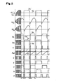
- the waveforms shown at A-H are output voltage waveforms appearing at the various points in Fig. 1.
- Fig. 2 shows the bridge inverter of Fig. 1 oscillating and also shows waveforms with the axis of the time enlarged from time t 0 .
- the operation at time t 1 onward will be described.
- the base drive signal F for the transistor 7 disappears and the base drive circuit 20 gives a reverse bias voltage changed from the forward bias voltage to the base terminal of the transistor 7.
- the reverse bias voltage is given to the base of the transistor 7, the base current of the transistor 7 shown at iB2 of IBL in F ig. 2 flows and when the collected carrier is discharged, the transistor 7 is turned off.
- the collector voltage rises.
- the comparator circuit 22 since the timing capacitor 16 discharges, the comparator circuit 22 has its output D reversed to take the L level, thus opening the drive logic circuits 18 and 19.
- the drive logic circuit 19 has been selected, it has the output A of the inhibition circuit 14 transferred thereto, so that the drive logic circuit 19 is inhibited for the duration corresponding to the pulse width of this output A.
- the output G takes the H level and the base current i BH which drives the drive circuit 21 and transistor 6 begins to flow.
- the point at which the base current i BH begins to flow is set during the time a current is flowing through the diode 6 of the inverter, said current through the diode 6 having a waveform shown at iC/D in Fig. 2 because of the free oscillation of the resonance capacitors 4 and 5 and induction heating coil 10.
- the output H of the malfunction preventing logic circuit 24 takes the L level, putting the inhibition circuit 14 in the inhibition state to prevent it from accepting output signals from the V CE detection circuit 13.
- the base current to be produced next is delayed for the time (t 2 -t 3 ) during which the inhibition circuit 14 is producing the output A; this duration is provided in order to wait for the time when the rising of the collector voltage is completed by the turn-off of the transistor 6 or 7, and this duration is not necessary if the switching elements are capable of ideal switching action.
- the timing capacitor 16 begins to charge (B waveform in Fig. 2).
- Fig. 3 is an electric wiring diagram forming a concrete embodiment of Fig. 1 of the invention.
- the numerals 25, 26, 37, 39, 52, and 67 denote diodes, and 27, 28, 31, 32, 35, 36, 39, 42, 44, 45, 47-51, 60, 61, 64, 66 and 69 denote resistors.
- the numerals 33, 34, and 63 denote capacitors; 29, 30, 53, and 68 denote voltage comparators; and 41 denotes a zener diode.
- the numeral 40 denotes an AND circuit; 54 denotes a NOT circuit; 55 denotes an OR circuit; 56 denotes a T flip-flop; and 57, 59 and 70 denote 3-input and 2-input NOR circuits.
- the numerals 43, 46 and 62 denote transistors, and 65 denotes a pulse transistor.
- the blocks and voltage output signals (A-H) having the same functions as in Fig. 1 are marked with like numerals.
- a description of the drive circuit 21 is omitted since it is the same as the drive circuit 20.
- V CE detection circuit 13 when V CE ' and V C3 ' cross each other, a rising signal is produced at the output of one of the two voltage comparators 29 and 30 and a falling signal at the output of the other. These rising and falling signals are differentiated by the resistors 31 and 32 and capacitors.33 and 34. The differentiated signals are such that only the pulses of positive direction are produced at both ends of the resistor 39 by the diodes 37 and 38.
- the inhibition circuit 14 is an AND circuit whose operation is well-known, and a_description thereof is omitted.
- the timing circuit 16 comprises a constant current charging circuit in- - cluding the zener diode 41, resistors 42 and 44 and transistor 43, a discharging circuit for the timing capacitor 16 including - the resistor 45 and transistor 46, and an oscillation circuit including the resistors 47-51, diode 52 and voltage comparator 53.
- the timing capacitor 16 begins to charge owing to the constant current charging circuit, and when the inhibition circuit 14 produces an output pulse, the transistor 46 is turned on and the timing capacitor 16 quickly discharges.
- the timing with which the inhibition circuit 14 produces output pulses is shorter than the oscillation period of the oscillation circuit; normally, the oscillation circuit does not operate and the output of the voltage comparator circuit 53 is at H level, while the output of the NOT circuit 54 remains at L level.
- the T flip-flop circuit 17 comprises a T flip-flop having two trigger inputs and is so arranged that when a rising input signal is imparted to either input, the outputs Q and Q are reversed.
- the drive logic circuits 18 and 19 and the NOR circuit of the malfunction preventing logic circuit 24 are well-known, and a description thereof is omitted.
- the drive circuits 20 and 21 form a base driving circuit using a pulse transformer. For example, in the drive circuit 20, when the transistor 62 is turned on, a forward base bias current flows through the transistor 7 of the inverter, and when it is turned off, the reverse electromotive force of the pulse transformer 65 applies a reverse base bias voltage.
- the comparator circuit 22 comprises the voltage comparator 68 and its output will be at L level if the voltage of the timing capacitor 16 is lower than the voltage at the terminal 23.
- the rising or falling of the collector voltage of a transistor of a bridge inverter is detected and then the next transistor is driven.
- the transistor discharges the collected carrier to turn off and the rise of the collector voltage (if the transistor on the opposite side is turned off, the falling of the collector voltage of the detection transistor) is detected.
- the simultaneous conduction of the series-connected transistors can be prevented.
- the switching time of the drive timing can be reduced to the extent allowed by the maximum capacity of the transistor, the resulting inverter device is high in operating efficiency.
- the invention has constructed a transistor type inverter for switching elements, but the same operation can be attained by using gate turn-off thyristors capable of turning off at the gate terminal. Further, according to the invention, it is possible to provide a highly stable device which will not accept erroneous trigger signals from the outside in that when a drive signal is produced at a transistor of the inverter, the turn-off detection pulse input of the transistor is inhibited.
Abstract
Description
- This invention relates to a bridge inverter for use in induction heating apparatuses having large load variations, particularly induction heating cooking appliances.
- Generally, in the inverter device for induction heating cooking appliances, since the load is in the form of a pan, stabilized operation is required irrespective of the material of the pan and irrespective of the presence or absence of a pan. Further, as is known in the art, the bridge inverter comprises a plurality of series-connected switching elements connected to a power source, the output from said converter being obtained at the junction of the series connection, said switching elements being alternately or successively driven. This inverter, however, has drawbacks; for example, when the switching time of the elements is prolonged by a temperature increase or when there is a large variation in load, there is the danger of the switching elements being simultaneously rendered conductive and thereby damaged. As a solution to this problem, the common means is to provide a fixed dwell period for stopping all the switching elements at the drive signal switching time in consideration of the amount of variation when the switching time varies. This means, however, does not essentially eliminate the danger of simultaneous conduction, and the provision of the sufficient dwell period has been the major cause of reduction of the operating efficiency of the inverter device. On the other hand, when an erroneous input signal is transferred to the control circuit, this is very undesirable since it leads to the simultaneous conduction of the switching elements of the inverter device or to abnormal oscillation thereof if the signal is on the level of not damaging the elements. As a solution to this problem, the common means is to stabilize the circuit by using a capacitor or the like which bypasses erroneous input signals. This means, however, depends on the correlation between the capacitance of the capacitor and the magnitude of the erroneous input signal, and can hardly serve as a radical solution to the problem.
- The present invention provides an inverter device which operates in an efficient and stable manner, rarely malfunctioning, despite variations in load and in the parameters of the switching elements of the inverter device. Thus, it provides a bridge inverter device which functions on the principle of detecting the complete turn-off of one of two switching elements by rising and falling voltage signals at both ends and then driving the other switching element. Concerning erroneous input signals, during driving of either switching element, any input signal from the inverter is inhibited to ensure that essentially there is no simultaneous conduction taking place even if there is a variation in the characteristics of the switching elements or an initial variation. Further, inverter device is highly stable against malfunction and abnormal oscillation.
-
- Fig. 1 is a block diagram showing an inverter device for induction heating according to an embodiment of the invention;
- Fig. 2 is a waveform diagram showing the operation of Figs. 1 and 3; and
- Fig. 3 is an electric circuit diagram showing a concrete electric circuit for the device.
- The arrangement will be described with reference to Fig. 1. The
numeral 1 denotes a commercial AC voltage source; 2 denotes a full-wave rectifier; and 3 denotes a filter capacitor, these parts constituting a rectifier circuit. Thenumeral 4 and 5 denote resonance capacitors, and 6 and 7 denote switching elements, which are transistors in this embodiment and will be hereinafter referred to as transistors. The numeral 8 and 9 denote diodes connected in antiparallel withsaid transistors numeral 10 denotes an induction heating and 11 denotes a cooking pan, these parts constituting a bridge inverter circuit. Thenumeral capacitor 3 and the collector of thetransistor 7, respectively, dividing the respective voltages. Thenumeral 13 denotes a VCE detection circuit wherein thecapacitor 3 and the collector voltage of thetransistor 7 are connected to the input terminal through theresistors transistor 7. Thenumeral 14 denotes an inhibition circuit using the output terminal of the VCE detection circuit 13 as its input, its output terminal determining whether or not to pass the output from the VCE detection circuit 13 on the basis of the signal level at a control input terminal H. Thenumeral 15 denotes a timing circuit and a backup oscillator (hereinafter referred to as timing circuit) using the output A of theinhibition circuit 14 as its trigger input, with atiming capacitor 16 being connected to the timing input terminal, the output being connected to one of the trigger terminals of a T flip-flop 17, saidtiming capacitor 16 being adapted to be caused to discharge and reset by means of the output A of theinhibition circuit 14. On the other hand, the backup oscillator is provided for forcibly changing the driving order if the detection voltage adjacent the zero phase of the commercial power source should be too low to actuate the VCE detection circuit 13, hte arrangement being such that it is prevented from operating during the time thetiming capacitor 16 is reset by the output from theinhibition circuit 14. Thenumeral 16 denotes the timing capacitor connected to saidtiming circuit 15 and to acomparator circuit 21, Thenumeral 17 denotes the T flip-flop, having two trigger inputs to which the output A of theinhibition circuit 14 and the output of thetiming circuit 15 are connected, the arrangement being such that normally thetiming circuit 15 produces no output and the T flip-flop will be triggered and reversed by the output A of theinhibition circuit 14, the outputs Q and Q being connected to drivelogic circuits numerals inhibition circuit 14, outputs Q and Q of the T flip-flop 17 and the output D of thecomparator 21 are connected to the input terminals, the arrangement being such that the drive logic circuit which is selected by the T flip-flop operates for a period of time determined by the output D of thecomparator 21 and the output A of theinhibition circuit 14. Thenumeral drive logic circuits transistors numeral 22 denotes a comparator circuit to make a comparison between the voltage of thetiming capacitor 16 and a reference voltage (at a terminal 23) imparted from the outside, to thereby determine the period of operation of thedrive logic circuits numeral 23 denotes the reference voltage terminal of thecomparator circuit 22 fed with a voltage from the outside, said terminal acting to open thedrive logic circuit timing capacitor 16 is lower than the reference voltage. Thenumeral 24 denotes a malfunction preventing logic circuit, with the outputs F and G of thedrive logic circuits inhibition circuit 14, it being noted that any output signal from theinhibition circuit 14 is inhibited when the output F or G is producing a signal. - In the above arrangement, the operation will now be described with reference to Figs. 1 and 2. In Fig. 2, VCE' and VC3' are signal input waveforms provided by dividing the collector voltage VCE of the
transistor 7 and the voltage VC3 of thecapacitor 3. The character iE/D is the waveform of current flowing through the antiparallel circuit of thetransistor 7 and diode 9. The character iC/D is the waveform of current flowing through the antiparallel circuit of thetransistor 6 and diode 8. The character iBL is the base drive current through thetransistor 7 and iBH is the base drive current throughte transistor 6. In the figure, the forward bias current is indicated at IB1 and the reverse bias current at IB2. The waveforms shown at A-H are output voltage waveforms appearing at the various points in Fig. 1. - Fig. 2 shows the bridge inverter of Fig. 1 oscillating and also shows waveforms with the axis of the time enlarged from time t0. For the purpose of explanation of the operation, the operation at time t1 onward will be described. At time tl, the base drive signal F for the
transistor 7 disappears and thebase drive circuit 20 gives a reverse bias voltage changed from the forward bias voltage to the base terminal of thetransistor 7. When the reverse bias voltage is given to the base of thetransistor 7, the base current of thetransistor 7 shown at iB2 of IBL in Fig. 2 flows and when the collected carrier is discharged, thetransistor 7 is turned off. When thetransistor 7 is turned off, the collector voltage rises. That is, at time t2, when the collector detection voltage VCE' of thetransistor 7 crosses the detection voltage VC3' of thecapacitor 3, a pulse output is produced at the output of the VCE detection circuit 13. At this time, the output H of the malfunction preventinglogic circuit 24 keeps theinhibition circuit 14 open at H level (the operation at this point will be later described), and the output pulse from the VCE detection circuit is given to thetiming circuit 15 and T flip-flop circuit 17 through the inhibition circuit 14 (time t2' A waveform). As soon as thetiming capacitor 16 is discharged, the T flip-flop 17 is reversed, whereby thedrive logic circuit 18 selected so far is replaced by thedrive logic circuit 19. On the other hand, since thetiming capacitor 16 discharges, thecomparator circuit 22 has its output D reversed to take the L level, thus opening thedrive logic circuits drive logic circuit 19 has been selected, it has the output A of theinhibition circuit 14 transferred thereto, so that thedrive logic circuit 19 is inhibited for the duration corresponding to the pulse width of this output A. When said output A terminates (at time t3), the output G takes the H level and the base current iBH which drives thedrive circuit 21 andtransistor 6 begins to flow. The point at which the base current iBH begins to flow is set during the time a current is flowing through thediode 6 of the inverter, said current through thediode 6 having a waveform shown at iC/D in Fig. 2 because of the free oscillation of theresonance capacitors 4 and 5 andinduction heating coil 10. At time t3, since a signal at H level is generated at the output G of thedrive logic circuit 19, the output H of the malfunction preventinglogic circuit 24 takes the L level, putting theinhibition circuit 14 in the inhibition state to prevent it from accepting output signals from the VCE detection circuit 13. In addition, the base current to be produced next is delayed for the time (t2-t3) during which theinhibition circuit 14 is producing the output A; this duration is provided in order to wait for the time when the rising of the collector voltage is completed by the turn-off of thetransistor timing capacitor 16 is terminated at time t3 by the output A of theinhibition circuit 14, thetiming capacitor 16 begins to charge (B waveform in Fig. 2). When the voltage (B waveform) of thetiming capacitor 16 reaches the voltage (C waveform) at thereference terminal 23 of the comparator circuit 22 (at time t4), the output D of thecomparator circuit 22 changes from L level to H level, putting thedrive logic circuit 19 in the inhibition state, with the output G taking the L level, thus stopping thedrive circuit 21 and imparting a reverse bias voltage to the base of thetransistor 6, whereupon the base current waveform iBH begins to have IB2 discharging the collected carrier. On the other hand, at this time t4, since the output G of aforesaiddrive logic circuit 19 disappears, the output H of the malfunction preventinglogic circuit 24 is brought to H level, putting theinhibition circuit 14 in the open state to enable it to accept output pulses from the VCE detection circuit 13. Upon termination of said reverse base bias current IB2 of thetransistor 6, the latter turns off (time t5) and, though not shown in Fig. 2, the collector-emitter voltage of thetransistor 6 rises. When the collector-emitter voltage of thetransistor 6 rises, since thetransistors transistor 7 drops. If this drop results in the input voltage of the VCE detection circuit 13 crossing the division voltage VC3' of thecapacitor 3, a pulse output is produced at the output of the VCE detection circuit, while a pulse voltage is produced at the output A of theinhibition circuit 14. Upon production of the output A of theinhibition circuit 14, thetiming capacitor 16 is discharged and at the same time the T flip-flop 17 is reversed (E waveform, time t 5) and thedrive logic circuit 18 is selected. Upon termination of the output A of the inhibition circuit 14 (time t6), the output F of thedrive logic circuit 18 takes the H level, actuating thedrive circuit 20 to turn off thetransistor 7, with the output F bringing the output H of the malfunction preventinglogic circuit 24 to L level and putting theinhibition circuit 14 in the inhibition state. When the charging (B waveform) of thetiming capacitor 16 reaches the reference voltage (C waveform) of the comparator circuit 22 (time t7), the base drive current of thetransistor 7 terminates, and the same operation is repeated henceforth. - The arrangement of Fig. 3 will now be described. Fig. 3 is an electric wiring diagram forming a concrete embodiment of Fig. 1 of the invention. In Fig. 3, the
numerals numerals 33, 34, and 63 denote capacitors; 29, 30, 53, and 68 denote voltage comparators; and 41 denotes a zener diode. The numeral 40 denotes an AND circuit; 54 denotes a NOT circuit; 55 denotes an OR circuit; 56 denotes a T flip-flop; and 57, 59 and 70 denote 3-input and 2-input NOR circuits. Thenumerals drive circuit 21 is omitted since it is the same as thedrive circuit 20. - In the above arrangement, the operations of the blocks will now be described in brief.
- In the VCE detection circuit 13, when VCE' and VC3' cross each other, a rising signal is produced at the output of one of the two
voltage comparators resistors diodes 37 and 38. Theinhibition circuit 14 is an AND circuit whose operation is well-known, and a_description thereof is omitted. Thetiming circuit 16 comprises a constant current charging circuit in- - cluding thezener diode 41, resistors 42 and 44 andtransistor 43, a discharging circuit for thetiming capacitor 16 including - the resistor 45 andtransistor 46, and an oscillation circuit including the resistors 47-51,diode 52 andvoltage comparator 53. Thetiming capacitor 16 begins to charge owing to the constant current charging circuit, and when theinhibition circuit 14 produces an output pulse, thetransistor 46 is turned on and thetiming capacitor 16 quickly discharges. The timing with which theinhibition circuit 14 produces output pulses is shorter than the oscillation period of the oscillation circuit; normally, the oscillation circuit does not operate and the output of thevoltage comparator circuit 53 is at H level, while the output of theNOT circuit 54 remains at L level. The T flip-flop circuit 17 comprises a T flip-flop having two trigger inputs and is so arranged that when a rising input signal is imparted to either input, the outputs Q and Q are reversed. Thedrive logic circuits logic circuit 24 are well-known, and a description thereof is omitted. Thedrive circuits drive circuit 20, when thetransistor 62 is turned on, a forward base bias current flows through thetransistor 7 of the inverter, and when it is turned off, the reverse electromotive force of thepulse transformer 65 applies a reverse base bias voltage. Thecomparator circuit 22 comprises thevoltage comparator 68 and its output will be at L level if the voltage of thetiming capacitor 16 is lower than the voltage at the terminal 23. - According to the present invention, the rising or falling of the collector voltage of a transistor of a bridge inverter is detected and then the next transistor is driven. Thus, even when the collection time of the transistor is prolonged owing to a rise in the temperature of the element or is caused to vary owing to initial variations, the transistor discharges the collected carrier to turn off and the rise of the collector voltage (if the transistor on the opposite side is turned off, the falling of the collector voltage of the detection transistor) is detected. As a result, the simultaneous conduction of the series-connected transistors can be prevented. Further, since the switching time of the drive timing can be reduced to the extent allowed by the maximum capacity of the transistor, the resulting inverter device is high in operating efficiency. In addition, the invention has constructed a transistor type inverter for switching elements, but the same operation can be attained by using gate turn-off thyristors capable of turning off at the gate terminal. Further, according to the invention, it is possible to provide a highly stable device which will not accept erroneous trigger signals from the outside in that when a drive signal is produced at a transistor of the inverter, the turn-off detection pulse input of the transistor is inhibited.
Claims (3)
Applications Claiming Priority (2)
| Application Number | Priority Date | Filing Date | Title |
|---|---|---|---|
| JP176871/81 | 1981-11-04 | ||
| JP56176871A JPS5878386A (en) | 1981-11-04 | 1981-11-04 | Induction heating inverter unit |
Publications (3)
| Publication Number | Publication Date |
|---|---|
| EP0092588A1 true EP0092588A1 (en) | 1983-11-02 |
| EP0092588A4 EP0092588A4 (en) | 1984-04-06 |
| EP0092588B1 EP0092588B1 (en) | 1988-02-10 |
Family
ID=16021248
Family Applications (1)
| Application Number | Title | Priority Date | Filing Date |
|---|---|---|---|
| EP82903256A Expired EP0092588B1 (en) | 1981-11-04 | 1982-11-02 | Induction heating inverter device |
Country Status (7)
| Country | Link |
|---|---|
| US (1) | US4555608A (en) |
| EP (1) | EP0092588B1 (en) |
| JP (1) | JPS5878386A (en) |
| AU (1) | AU552574B2 (en) |
| CA (1) | CA1205869A (en) |
| DE (1) | DE3278111D1 (en) |
| WO (1) | WO1983001721A1 (en) |
Cited By (7)
| Publication number | Priority date | Publication date | Assignee | Title |
|---|---|---|---|---|
| EP0460279A2 (en) * | 1990-06-07 | 1991-12-11 | Matsushita Electric Industrial Co., Ltd. | Induction heating cooker |
| FR2669174A1 (en) * | 1990-11-12 | 1992-05-15 | Lunard Henri Yves | Rectifier circuit for induction heating appliance |
| GB2265505A (en) * | 1992-03-19 | 1993-09-29 | Chen Su Min | Push-pull induction heating drive circuit |
| EP0583519A1 (en) * | 1992-08-18 | 1994-02-23 | Superluck Electrics Corp. | Dual push-pull heating device of induction cooker having multiple burners |
| US5488214A (en) * | 1992-03-14 | 1996-01-30 | E.G.O. Elektro-Gerate Blanc U. Fischer | Inductive cooking point heating system |
| GB2520922A (en) * | 2013-10-15 | 2015-06-10 | Trung Van Ta | Battery powered food or beverage induction heater |
| CN108731040A (en) * | 2017-04-14 | 2018-11-02 | 佛山市顺德区美的电热电器制造有限公司 | The control method and device of electromagnetic heating cookware |
Families Citing this family (10)
| Publication number | Priority date | Publication date | Assignee | Title |
|---|---|---|---|---|
| US4885447A (en) * | 1985-01-23 | 1989-12-05 | Balay, S.A. | System for the induction heating of the electric plates of a cooker |
| US4945467A (en) * | 1988-02-26 | 1990-07-31 | Black & Decker Inc. | Multiple-mode voltage converter |
| US5004881A (en) * | 1989-11-22 | 1991-04-02 | Goldstar Co., Ltd. | Method and circuit for controlling power level in the electromagnetic induction cooker |
| EP0666703A1 (en) * | 1994-02-08 | 1995-08-09 | HUANG, Wen-Liang | Power transistor driving circuit of electromagnetic induction heating device |
| KR970006379B1 (en) * | 1994-05-17 | 1997-04-25 | 엘지전자 주식회사 | Power control circuit of inverter |
| US6657170B2 (en) * | 2001-05-21 | 2003-12-02 | Thermal Solutions, Inc. | Heat retentive inductive-heatable laminated matrix |
| US6953919B2 (en) | 2003-01-30 | 2005-10-11 | Thermal Solutions, Inc. | RFID-controlled smart range and method of cooking and heating |
| US7573005B2 (en) | 2004-04-22 | 2009-08-11 | Thermal Solutions, Inc. | Boil detection method and computer program |
| US10182472B2 (en) | 2011-12-29 | 2019-01-15 | Arcelik Anonim Sirketi | Wireless kitchen appliance operated on induction heating cooker |
| US10129935B2 (en) * | 2011-12-29 | 2018-11-13 | Arcelik Anonim Sirketi | Wireless kitchen appliance operated on an induction heating cooker |
Citations (6)
| Publication number | Priority date | Publication date | Assignee | Title |
|---|---|---|---|---|
| FR2160362A1 (en) * | 1971-11-19 | 1973-06-29 | Gen Electric | |
| FR2338618A1 (en) * | 1976-01-14 | 1977-08-12 | Matsushita Electric Ind Co Ltd | INDUCTION HEATING APPLIANCE EQUIPPED WITH MEANS TO DETECT THE GOING TO ZERO OF A HIGH FREQUENCY OSCILLATION TO DETERMINE THE TRIP TIME |
| JPS5296316A (en) * | 1976-02-09 | 1977-08-12 | Densetsu Kiki Kogyo Kk | Inverter circuit |
| DE2836610A1 (en) * | 1978-08-22 | 1980-03-06 | Licentia Gmbh | Induction heater with power transistor switches - supplying resonant circuit containing heating coil and controlled, current-limiting choke |
| FR2446557A1 (en) * | 1979-01-15 | 1980-08-08 | Sachs Systemtechnik Gmbh | SINUSOIDAL POWER GENERATOR |
| GB2056795A (en) * | 1979-08-03 | 1981-03-18 | Tokyo Shibaura Electric Co | Inductive heating apparatus |
Family Cites Families (4)
| Publication number | Priority date | Publication date | Assignee | Title |
|---|---|---|---|---|
| US3898410A (en) * | 1972-06-16 | 1975-08-05 | Environment One Corp | AC to RF converter circuit for induction cooking unit |
| JPS51128746A (en) * | 1975-05-02 | 1976-11-09 | Toshiba Corp | Metiod of induction heating for range |
| US4115677A (en) * | 1975-10-02 | 1978-09-19 | Tokyo Shibaura Electric Co., Ltd. | Induction heating apparatus |
| JP3157267B2 (en) * | 1992-04-21 | 2001-04-16 | マツダ株式会社 | Vehicle power transmission |
-
1981
- 1981-11-04 JP JP56176871A patent/JPS5878386A/en active Granted
-
1982
- 1982-11-02 US US06/522,373 patent/US4555608A/en not_active Expired - Lifetime
- 1982-11-02 DE DE8282903256T patent/DE3278111D1/en not_active Expired
- 1982-11-02 EP EP82903256A patent/EP0092588B1/en not_active Expired
- 1982-11-02 AU AU90538/82A patent/AU552574B2/en not_active Ceased
- 1982-11-02 WO PCT/JP1982/000426 patent/WO1983001721A1/en active IP Right Grant
- 1982-12-23 CA CA000418502A patent/CA1205869A/en not_active Expired
Patent Citations (6)
| Publication number | Priority date | Publication date | Assignee | Title |
|---|---|---|---|---|
| FR2160362A1 (en) * | 1971-11-19 | 1973-06-29 | Gen Electric | |
| FR2338618A1 (en) * | 1976-01-14 | 1977-08-12 | Matsushita Electric Ind Co Ltd | INDUCTION HEATING APPLIANCE EQUIPPED WITH MEANS TO DETECT THE GOING TO ZERO OF A HIGH FREQUENCY OSCILLATION TO DETERMINE THE TRIP TIME |
| JPS5296316A (en) * | 1976-02-09 | 1977-08-12 | Densetsu Kiki Kogyo Kk | Inverter circuit |
| DE2836610A1 (en) * | 1978-08-22 | 1980-03-06 | Licentia Gmbh | Induction heater with power transistor switches - supplying resonant circuit containing heating coil and controlled, current-limiting choke |
| FR2446557A1 (en) * | 1979-01-15 | 1980-08-08 | Sachs Systemtechnik Gmbh | SINUSOIDAL POWER GENERATOR |
| GB2056795A (en) * | 1979-08-03 | 1981-03-18 | Tokyo Shibaura Electric Co | Inductive heating apparatus |
Non-Patent Citations (1)
| Title |
|---|
| See also references of WO8301721A1 * |
Cited By (10)
| Publication number | Priority date | Publication date | Assignee | Title |
|---|---|---|---|---|
| EP0460279A2 (en) * | 1990-06-07 | 1991-12-11 | Matsushita Electric Industrial Co., Ltd. | Induction heating cooker |
| EP0460279A3 (en) * | 1990-06-07 | 1991-12-27 | Matsushita Electric Industrial Co., Ltd. | Induction heating cooker |
| US5319174A (en) * | 1990-06-07 | 1994-06-07 | Matsushita Electric Industrial Co., Ltd. | Induction heating cooker with constant frequency controlled inverter |
| FR2669174A1 (en) * | 1990-11-12 | 1992-05-15 | Lunard Henri Yves | Rectifier circuit for induction heating appliance |
| US5488214A (en) * | 1992-03-14 | 1996-01-30 | E.G.O. Elektro-Gerate Blanc U. Fischer | Inductive cooking point heating system |
| GB2265505A (en) * | 1992-03-19 | 1993-09-29 | Chen Su Min | Push-pull induction heating drive circuit |
| GB2265505B (en) * | 1992-03-19 | 1995-10-11 | Chen Su Min | Dual push-pull induction heating drive circuit |
| EP0583519A1 (en) * | 1992-08-18 | 1994-02-23 | Superluck Electrics Corp. | Dual push-pull heating device of induction cooker having multiple burners |
| GB2520922A (en) * | 2013-10-15 | 2015-06-10 | Trung Van Ta | Battery powered food or beverage induction heater |
| CN108731040A (en) * | 2017-04-14 | 2018-11-02 | 佛山市顺德区美的电热电器制造有限公司 | The control method and device of electromagnetic heating cookware |
Also Published As
| Publication number | Publication date |
|---|---|
| EP0092588B1 (en) | 1988-02-10 |
| AU9053882A (en) | 1983-05-18 |
| US4555608A (en) | 1985-11-26 |
| DE3278111D1 (en) | 1988-03-17 |
| CA1205869A (en) | 1986-06-10 |
| EP0092588A4 (en) | 1984-04-06 |
| JPS5878386A (en) | 1983-05-11 |
| AU552574B2 (en) | 1986-06-05 |
| JPS6349874B2 (en) | 1988-10-06 |
| WO1983001721A1 (en) | 1983-05-11 |
Similar Documents
| Publication | Publication Date | Title |
|---|---|---|
| US4555608A (en) | Inverter device for induction heating | |
| US4145592A (en) | Induction heating apparatus with means for detecting zero crossing point of high-frequency oscillation to determine triggering time | |
| EP0373693B1 (en) | Generator of drive signals for transistors connected in a half-bridge configuration | |
| KR100541724B1 (en) | power supply apparatus for motor and controlling method thereof | |
| US4562383A (en) | Converter | |
| US4368414A (en) | Pulse motor driving device of sewing machines | |
| US4338503A (en) | Inductive heating apparatus | |
| US4358654A (en) | Static power switching system for induction heating | |
| US20040165322A1 (en) | Relay contact protection | |
| US4612611A (en) | Starting circuit for a parallel resonant circuit inverter | |
| JP5632613B2 (en) | Electric motor power control | |
| US3953780A (en) | Inverter having forced turn-off | |
| US4096559A (en) | Power supply circuit | |
| JPH07115768A (en) | Resonance type converter | |
| US4262213A (en) | Universal power module | |
| US4051386A (en) | Frequency doubling circuit | |
| JPS6349875B2 (en) | ||
| US3441831A (en) | Dc to ac converter | |
| CN217282898U (en) | Pulse width adjustable synchronous drive MOSFET electronic switch | |
| RU2025881C1 (en) | A c converter for supply of inductor | |
| JPS6226157B2 (en) | ||
| JPS6161508B2 (en) | ||
| JPH03207263A (en) | Switching power supply | |
| JP2828521B2 (en) | Inductive load current controller | |
| JPS5849087A (en) | Inverter device |
Legal Events
| Date | Code | Title | Description |
|---|---|---|---|
| PUAI | Public reference made under article 153(3) epc to a published international application that has entered the european phase |
Free format text: ORIGINAL CODE: 0009012 |
|
| 17P | Request for examination filed |
Effective date: 19830706 |
|
| AK | Designated contracting states |
Designated state(s): DE FR GB |
|
| 17Q | First examination report despatched |
Effective date: 19860303 |
|
| GRAA | (expected) grant |
Free format text: ORIGINAL CODE: 0009210 |
|
| AK | Designated contracting states |
Kind code of ref document: B1 Designated state(s): DE FR GB |
|
| REF | Corresponds to: |
Ref document number: 3278111 Country of ref document: DE Date of ref document: 19880317 |
|
| ET | Fr: translation filed | ||
| PLBE | No opposition filed within time limit |
Free format text: ORIGINAL CODE: 0009261 |
|
| STAA | Information on the status of an ep patent application or granted ep patent |
Free format text: STATUS: NO OPPOSITION FILED WITHIN TIME LIMIT |
|
| 26N | No opposition filed | ||
| PGFP | Annual fee paid to national office [announced via postgrant information from national office to epo] |
Ref country code: GB Payment date: 19941025 Year of fee payment: 13 |
|
| PGFP | Annual fee paid to national office [announced via postgrant information from national office to epo] |
Ref country code: FR Payment date: 19941109 Year of fee payment: 13 |
|
| PGFP | Annual fee paid to national office [announced via postgrant information from national office to epo] |
Ref country code: DE Payment date: 19941110 Year of fee payment: 13 |
|
| PG25 | Lapsed in a contracting state [announced via postgrant information from national office to epo] |
Ref country code: GB Effective date: 19951102 |
|
| GBPC | Gb: european patent ceased through non-payment of renewal fee |
Effective date: 19951102 |
|
| PG25 | Lapsed in a contracting state [announced via postgrant information from national office to epo] |
Ref country code: FR Effective date: 19960731 |
|
| PG25 | Lapsed in a contracting state [announced via postgrant information from national office to epo] |
Ref country code: DE Effective date: 19960801 |
|
| REG | Reference to a national code |
Ref country code: FR Ref legal event code: ST |