EP0092214B1 - Circuit for the acquittance of calling signals by emitting confirmation signals in an exchange, in particular in a data and telex exchange - Google Patents
Circuit for the acquittance of calling signals by emitting confirmation signals in an exchange, in particular in a data and telex exchange Download PDFInfo
- Publication number
- EP0092214B1 EP0092214B1 EP83103731A EP83103731A EP0092214B1 EP 0092214 B1 EP0092214 B1 EP 0092214B1 EP 83103731 A EP83103731 A EP 83103731A EP 83103731 A EP83103731 A EP 83103731A EP 0092214 B1 EP0092214 B1 EP 0092214B1
- Authority
- EP
- European Patent Office
- Prior art keywords
- signals
- signal
- data
- register
- data signals
- Prior art date
- Legal status (The legal status is an assumption and is not a legal conclusion. Google has not performed a legal analysis and makes no representation as to the accuracy of the status listed.)
- Expired
Links
Images
Classifications
-
- H—ELECTRICITY
- H04—ELECTRIC COMMUNICATION TECHNIQUE
- H04L—TRANSMISSION OF DIGITAL INFORMATION, e.g. TELEGRAPHIC COMMUNICATION
- H04L12/00—Data switching networks
- H04L12/50—Circuit switching systems, i.e. systems in which the path is physically permanent during the communication
Definitions
- the invention relates to a circuit arrangement for acknowledging incoming call lines via data signals in the incoming transmission direction by issuing call confirmation signals in a switching system in which connection lines provided for the transmission of data signals in the incoming and outgoing transmission direction are connected to line connection circuits which are combined to form line groups are connected to data transmission devices controlling the data signal switching between the connecting lines, each connecting line group for the connecting lines transmitting the data signals in the outgoing transmission direction having a register arrangement from which a call confirmation signal is emitted immediately after a call signal has been determined and a notification signal indicating this determination has been issued.
- connection lines provided for the transmission of data signals in the incoming and outgoing transmission direction are connected to line connection circuits which are combined to form connection line groups and are connected to data transmission directions controlling the data signal switching between the line connection lines.
- call signals are acknowledged in that call confirmation signals are provided by centrally provided data transmission devices. It has now been shown that this measure is unsatisfactory if relatively heavy connection traffic has to be taken into account.
- a circuit arrangement for controlling data stations in data transmission systems is also known (DE-B2-2 903 646), in which, during the call to one of several stations with the aid of clock signals, initially several mutually identical synchronization characters and subsequently further characters are entered bit-serially into a shift register , at the steps of which a storage device is connected in parallel.
- the content of the shift register addresses the storage device in such a way that its output signals switch on a detector for the synchronization characters and, via this, a bit counter which can be switched on by the clock signals and which actuates a character counter connected downstream of it.
- this character counter After counting a predetermined number of synchronization characters via a further addressable storage device, this character counter switches off the detector for the synchronization characters and, after counting a predetermined number of additional characters, turns on a flip-flop for outputting a commissioning signal to a control device of the called station.
- the invention has for its object to design a circuit arrangement of the type mentioned so that the call confirmation signals can be provided and issued with little circuitry.
- the invention has the advantage of a particularly low outlay in terms of circuitry with regard to the implementation of the register arrangement and thus with regard to the delivery of the confirmation signals.
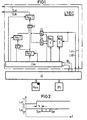
- FIG. 1 is in particular a data and telex switching system, as described in more detail at the point mentioned at the beginning.
- Centrally provided data transmission devices of this switching system are indicated in FIG. 1, which comprise a data transmission control arrangement CC, a working memory Mem and a processing unit or central processing unit CPU.
- Connection line groups are connected to these data transmission devices, in particular to the data transmission control arrangement CC, of which only a single line connection group LTEC is indicated in FIG. 1.
- connection lines are combined which transmit data signals in the incoming transmission direction or in the outgoing transmission direction.
- connection line group LTEC indicated in FIG. 1 two such lines are indicated: a connection line Lan supplying data signals in the incoming transmission direction and a connection line Lab emitting data signals in the outgoing transmission direction.
- a control arrangement Con is connected to the data transmission control arrangement CC via a bus line BL.
- the two control arrangements Con and CC in particular exchange commands or commands via this bus line BL.
- a register Reg1 is connected to the control arrangement Con via at least one control line, via which control signals can be fed to the register Reg1, upon the occurrence of which the register content contained in the relevant register Reg1 is output. If necessary, the register Reg1 is connected to the control arrangement Con with a charging input (dashed line) in order to be able to be charged separately via this connection. At this point it should be noted that the register content of the register Reg1 is given by a call confirmation signal.
- the register Reg1 is connected on the output side via an OR gate G1 to a signal or load input of a register Reg2, which is also connected to the control arrangement Con with a control input.
- the relevant OR gate G1 is also connected to the control arrangement Con with a further input.
- the register Reg1 and the register Reg2 are connected on the output side via a further OR gate G2 to the signal or load input of a further register Reg3, which is connected to the control arrangement Con with a control input. On the output side, this register Reg3 is connected to the line Lab carrying signals in the outgoing transmission direction.
- the relevant register Reg3 forms, together with the two registers Reg2 and Reg1, a register arrangement, the functioning of which will be discussed below with reference to the diagram shown in FIG. 2.
- level relationships are indicated, as may occur on the connection line Lan indicated in FIG. 1. It is assumed that a level change from binary state "0" to binary state “1” takes place. However, it should be noted here that in principle it is also possible to take into account another level change.
- the level change indicated in FIG. 2 is intended to be characteristic of the occurrence of a call state. This means that the signal occurring with the binary level "1" on the connecting line Lan represents a call signal.
- the call signal occurring on the connecting line Lan according to FIG. 1 is recorded on the basis of the circuit relationships indicated in FIG. 1 by the data transmission control arrangement CC provided there and recognized as a call signal.
- the relevant data transmission control arrangement CC then issues a message signal to the control arrangement Con of the line group LTEC, from which the relevant call signal has been received.
- it should be noted here it is in principle also possible to carry out a corresponding evaluation of the respective call signal in the associated line group.
- this register Reg1 contains a call confirmation signal.
- This call confirmation signal is now loaded via the OR gate G2 into the register Reg3 and also into the register Reg2.
- two call confirmation signals are thus emitted via the connecting line Lab.
- these call confirmation signals are issued at a point in time which is a time tx from the start of the occurrence of a Call signal on the connection line Lan is delayed. This time period tx can, for example, be less than 10 ms.
- the call signals emitted via the connecting line Lab according to FIG. 1 are indicated with Syn in the bottom line of the diagram according to FIG. 2; these signals are, for example, synchronization signals. In principle, however, any other signal can also be used as a call confirmation signal. 2 shows that with the delivery of the relevant call confirmation signal Syn there is a level change from the binary "1" vegetable to the binary "0" level on the connecting line Lab.
- the register Reg2 is normally used for the inclusion of a so-called space character, which, if required, for. B. in the idle state of the circuit arrangement to be delivered via the connecting line Lab.
- a blank character once loaded into the register Reg2 would be supplied to the register Reg3 in a non-destructive manner by control signals subsequently fed to the control input of this register Reg2, from which the respective blank character would then be output to the connecting line Lab.
- the call acknowledgment signal remains contained in the Reg1 register.
- the contents of these registers can only be changed by feeding changed signals to the signal or control inputs of these registers Reg2, Reg1.
- This circuit part comprises two registers Reg4, Reg5, of which the register Reg5 is connected with its signal or charging input to a supply line Lab 'which supplies signals and which is connected to the data transmission control arrangement CC.
- a signal input of an AND gate G3 is also connected to the feed line Lab 'in question, and is connected on the output side to an input of the OR gate G2 already mentioned.
- the register Reg5 is connected on the output side to the signal or load input of a register Reg4, which is connected on the output side to an input of an AND gate G4.
- This AND gate G4 is also connected to the input side of the OR gate G2.
- the two registers Reg4, Reg5 are connected to the control arrangement Con with control inputs.
- the AND gate G3 is connected with a negating input together with an input of the AND gate G4 to a further output of the control arrangement Con.
- the circuit section under consideration serves to buffer the data signals supplied via the supply line Lab 'and to be forwarded via the connecting line Lab, if necessary.
- the two registers Reg4, Reg5 are included in the connection in question.
- the AND gate G4 is controlled for transmission, while the AND gate G3 is blocked.
- Use is made of this intermediate buffering in the event that the supply of data signals via the supply line Lab 'does not take place cyclically, while the delivery of data signals via the connecting line Lab should take place cyclically.
- the circuit section under consideration provides time compensation between data signals recorded acyclically and data signals to be passed on cyclically. Such acyclic recording of data signals can occur, for example, if different numbers of connecting lines have to be taken into account with regard to the supply of data signals for successive data signal recording periods.
Abstract
Description
Die Erfindung bezieht sich auf eine Schaltungsanordnung zum Quittieren von über Datensignale in ankommender Übertragungsrichtung zuführenden Anschlußleitungen eintreffenden Anrufsignalen durch Abgabe von Anrufbestätigungssignalen in einer Vermittlungsanlage, in der für die Übertragung von Datensignalen in ankommender und abgehender Übertragungsrichtung vorgesehene Anschlußleitungen an Leitungsanschlußschaltungen angeschlossen sind, die zu Anschlußleitungsgruppen zusammengefaßt mit die Datensignalvermittlung zwischen den Anschlußleitungen steuernden Datenübertragungseinrichtungen verbunden sind, wobei jede Anschlußleitungsgruppe für die Datensignale in abgehender Übertragungsrichtung übertragenden Anschlußleitungen eine Registeranordnung aufweist, aus der ein Anrufbestätigungssignal sofort nach Ermittlung eines Anrufsignals und eines diese Ermittlung anzeigenden Meldesignals abgegeben wird.The invention relates to a circuit arrangement for acknowledging incoming call lines via data signals in the incoming transmission direction by issuing call confirmation signals in a switching system in which connection lines provided for the transmission of data signals in the incoming and outgoing transmission direction are connected to line connection circuits which are combined to form line groups are connected to data transmission devices controlling the data signal switching between the connecting lines, each connecting line group for the connecting lines transmitting the data signals in the outgoing transmission direction having a register arrangement from which a call confirmation signal is emitted immediately after a call signal has been determined and a notification signal indicating this determination has been issued.
Es ist bereits eine Schaltungsanordnung zum Quittieren von über Datensignale in ankommender Übertragungsrichtung zuführenden Anschlußleitungen eintreffenden Anrufsignalen durch Abgabe von Anrufbestätigungssignalen in einer Daten- und Fernschreibvermittlungsanlage bekannt ("Siemens-Zeitschrift", 51 (1977), Heft 1, Seiten 18 bis 27), bei der für die Übertragung von Datensignalen in ankommender und abgehender Übertragungsrichtung vorgesehene Anschlußleitungen an Leitungsanschlußschaltungen angeschlossen sind, die zu Anschlußleitungsgruppen zusammengefaßt mit die Datensignalvermittlung zwischen den Leitungsanschlußleitungen steuernden Datenübertragungsrichtungen verbunden sind. Bei dieser bekannten Schaltungsanordnung erfolgt das Quittieren von Anrufsignalen dadurch, daß Anrufbestatigungssignale von zentral vorgesehenen Datenübertragungseinrichtungen bereitgestellt werden. Es hat sich nun gezeigt, daß diese Maßnahme dann nicht zufriedenstellt, wenn ein relativ starker Verbindungsverkehr zu berucksichtigen ist. Überdies existieren Vorschriften bzw. Empfehlungen (siehe CCIII-Empfehlung X.71), die in Verbindung mit synchron arbeitenden Anschlußschaltungen zu berücksichtigen sind. Dabei existiert im speziellen Fall die Forderung, ein Anrufbestatigungssignal spätestens 10 ms nach Auftreten eines Anrufsignals abzugeben. Eine derartige Forderung ist jedoch bei der bisher bekannten Schaltungsanordnung nicht immer zu erfüllen.There is already a circuit arrangement for acknowledging incoming call signals via data signals in the incoming transmission direction by issuing call confirmation signals in a data and telex switching system ("Siemens-Zeitschrift", 51 (1977),
Es ist ferner eine Schaltungsanordnung zum Ansteuern von Datenstationen in Datenübertragungsanlagen bekannt (DE-B2-2 903 646), bei denen während der Anrufung einer von mehreren Stationen unter Mitwirkung von Taktsignalen zunächst mehrere einander identische Synchronisationszeichen und nachfolgend weitere Zeichen bitseriell in ein Schieberegister eingegeben werden, an dessen Stufen parallel ein Speichergerät angeschlossen ist. Der Inhalt des Schieberegisters adressiert das Speichergerät derart, daß dessen Ausgangssignale einen Detektor für die Synchronisationszeichen und über diesen einen von den Taktsignalen weiterschaltbaren Bitzähler einschalten, der einen ihm nachgeschalteten Zeichenzähler betätigt. Dieser Zeichenzähler schaltet nach Zählung einer vorgegebenen Anzahl von Synchronisationszeichen über ein weiteres adressierbares Speichergerät den Detektor für die Synchronisationszeichen ab, und er schaltet nach Zählung einer vorgegebenen Anzahl von weiteren Zeichen ein Flip-Flop zur Ausgabe eines Inbetriebnahmesignals an ein Steuergerät der angerufenen Station ein. Mit diesen Schaltungsmaßnahmen werden zwar nicht nur die einer Nachricht vorauslaufenden synchronisierenden oder adressierenden Signale erkannt, sondern es werden auch nachfolgende, der Nachricht vorauslaufende Standardzeichen zumindest hinsichtlich ihrer Anzahl ermittelt. Von Nachteil bei dieser bekannten Schaltungsanordnung ist jedoch deren relativ hoher schaltungstechnischer Aufwand hinsichtlich der Bereitstellung von Anrufbestätigungssignalen.A circuit arrangement for controlling data stations in data transmission systems is also known (DE-B2-2 903 646), in which, during the call to one of several stations with the aid of clock signals, initially several mutually identical synchronization characters and subsequently further characters are entered bit-serially into a shift register , at the steps of which a storage device is connected in parallel. The content of the shift register addresses the storage device in such a way that its output signals switch on a detector for the synchronization characters and, via this, a bit counter which can be switched on by the clock signals and which actuates a character counter connected downstream of it. After counting a predetermined number of synchronization characters via a further addressable storage device, this character counter switches off the detector for the synchronization characters and, after counting a predetermined number of additional characters, turns on a flip-flop for outputting a commissioning signal to a control device of the called station. With these circuit measures, not only are the synchronizing or addressing signals preceding a message recognized, but subsequent standard characters preceding the message are also determined, at least in terms of their number. A disadvantage of this known circuit arrangement, however, is its relatively high circuit complexity in terms of the provision of call confirmation signals.
Im Zusammenhang mit der Datensignalübertragung ist es auch schon bekannt ("Die Organisation von Datennetzen" , James Martin, Karl Hanser Verlag, München 1972, Seite 149), die in eine Verbindung einzubeziehende Datenstation daraufhin abzufragen, ob sie bereit ist, einen Datenblock zu empfangen. Diese Datenstation antwortet dann positiv oder negativ, indem sie ein Steuerzeichen oder eine Steuerzeichenfolge zurückschickt. Über den näheren Aufbau einer Schaltungsanordnung zum Quittieren von Abfragesignalen ist in diesem Zusammenhang jedoch nichts bekannt.In connection with data signal transmission, it is also known ("The Organization of Data Networks", James Martin, Karl Hanser Verlag, Munich 1972, page 149) to query the data station to be included in a connection as to whether it is ready to receive a data block . This terminal then responds positively or negatively by sending back a control character or a control character string. In this context, however, nothing is known about the more detailed structure of a circuit arrangement for acknowledging interrogation signals.
Es ist schließlich auch schon eine Schaltungsanordnung zur Aufnahme und Abgabe von Informationsdaten und Signalisierungsdaten in einer programmgesteuerten Vermittlungszentrale bekannt (DE-A-2 833 048). Bei dieser bekannten Schaltungsanordnung sind zwar Register für die Zwischenspeicherung von Signalen vorgesehen. Über irgendwelche Maßnahmen zum Quittieren von Abfragesignalen ist jedoch auch in diesem Zusammenhang nichts konkret bekannt.Finally, a circuit arrangement for receiving and delivering information data and signaling data in a program-controlled switching center is also known (DE-A-2 833 048). In this known circuit arrangement, registers are provided for the intermediate storage of signals. In this context, however, nothing is specifically known about any measures for acknowledging query signals.
Der Erfindung liegt die Aufgabe zugrunde, eine Schaltungsanordnung der eingangs genannten Art so auszugestalten, daß mit geringem schaltungstechnischen Aufwand die Anrufbestätigungssignale bereitgestellt und abgegeben werden können.The invention has for its object to design a circuit arrangement of the type mentioned so that the call confirmation signals can be provided and issued with little circuitry.
Gelöst wird die vorstehend aufgezeigte Aufgabe durch die im Anspruch 1 gekennzeichneten Maßnahmen.The object outlined above is achieved by the measures characterized in
Die Erfindung bringt den Vorteil eines besonders geringen schaltungstechnischen Aufwands hinsichtlich der Realisierung der Registeranordnung und damit im Hinblick auf die Abgabe der Bestätigungssignale mit sich.The invention has the advantage of a particularly low outlay in terms of circuitry with regard to the implementation of the register arrangement and thus with regard to the delivery of the confirmation signals.
Bei Ausgestaltung der Erfindung in der im Anspruch 2 gekennzeichneten Weise ergibt sich der Vorteil, daß auf relativ einfache Weise Verzögerungen bei der Aufnahme von Datensignalen von diese Datensignale zuführenden Anschlußleitungen bei der Weitergabe dieser Datensignale berücksichtigt werden können.In the embodiment of the invention in the manner characterized in
Anhand von Zeichnungen wird die Erfindung nachstehend beispielsweise näher erläutert.
- FIG 1 zeigt in einem Blockschaltbild eine Schaltungsanordnung gemäß der Erfindung.
- FIG 2 zeigt ein Signaldiagramm, anhand dessen die Arbeitsweise der in FIG 1 dargestellten Schaltungsanordnung erläutert wird.
- 1 shows in a block diagram a circuit arrangement according to the invention.
- 2 shows a signal diagram, on the basis of which the mode of operation of the circuit arrangement shown in FIG. 1 is explained.
In FIG 1 ist schematisch eine Vermittlungsanlage angedeutet, bei der es sich insbesondere um eine Daten- und Fernschreibvermittlungsanlage handelt, wie sie an der eingangs erwähnten Stelle näher beschrieben ist. Von dieser Vermittlungsanlage sind in FIG 1 zentral vorgesehene Datenübertragungseinrichtungen angedeutet, die eine Datenübertragungssteueranordnung CC, einen Arbeitsspeicher Mem und eine Verarbeitungseinheit bzw. Zentraleinheit CPU umfassen. An diesen Datenübertragungseinrichtungen, und zwar insbesondere an der Datenübertragungssteueranordnung CC sind Anschlußleitungsgruppen angeschlossen, von denen in Fig. 1 lediglich eine einzige Leitungsanschlußgruppe LTEC angedeutet ist. In den betreffenden Leitungsanschlußgruppen sind Anschlußleitungen zusammengefaßt, die Datensignale in ankommender Übertragungsrichtung bzw. in abgehender Übertragungsrichtung übertragen. Bei der in Fig. 1 angedeuteten Anschlußleitungsgruppe LTEC sind zwei derartige Leitungen angedeutet: Eine Datensignale in ankommender Übertragungsrichtung zuführende Anschlußleitung Lan und eine Datensignale in abgehender Übertragungsrichtung abgebende Anschlußleitung Lab.A switching system is indicated schematically in FIG. 1, which is in particular a data and telex switching system, as described in more detail at the point mentioned at the beginning. Centrally provided data transmission devices of this switching system are indicated in FIG. 1, which comprise a data transmission control arrangement CC, a working memory Mem and a processing unit or central processing unit CPU. Connection line groups are connected to these data transmission devices, in particular to the data transmission control arrangement CC, of which only a single line connection group LTEC is indicated in FIG. 1. In the relevant line connection groups, connection lines are combined which transmit data signals in the incoming transmission direction or in the outgoing transmission direction. In the connection line group LTEC indicated in FIG. 1, two such lines are indicated: a connection line Lan supplying data signals in the incoming transmission direction and a connection line Lab emitting data signals in the outgoing transmission direction.
Zu der Anschlußleitungsgruppe LTEC gehört gemäß eine Steueranordnung Con, die über eine Busleitung BL mit der Datenübertragungssteueranordnung CC verbunden ist. Über diese Busleitung BL tauschen die beiden Steueranordnungen Con und CC insbesondere Befehle bzw. Kommandos aus.According to the connecting line group LTEC, a control arrangement Con is connected to the data transmission control arrangement CC via a bus line BL. The two control arrangements Con and CC in particular exchange commands or commands via this bus line BL.
Mit der Steueranordnung Con ist ein Register Reg1 über wenigstens eine Steuerleitung verbunden, über die den Register Reg1 Steuersignale zuführbar sind, auf deren Auftreten hin der in dem betreffenden Register Reg1 enthaltene Registerinhalt abgegeben wird. Gegebenenfalls ist das Register Reg1 mit einem Ladeeingang an der Steueranordnung Con angeschlossen (gestrichelte Linie), um über diese Verbindung gesondert geladen werden zu können. An dieser Stelle sei angemerkt, daß der Registerinhalt des Registers Reg1 durch ein Anrufbestätigungssignal gegeben ist.A register Reg1 is connected to the control arrangement Con via at least one control line, via which control signals can be fed to the register Reg1, upon the occurrence of which the register content contained in the relevant register Reg1 is output. If necessary, the register Reg1 is connected to the control arrangement Con with a charging input (dashed line) in order to be able to be charged separately via this connection. At this point it should be noted that the register content of the register Reg1 is given by a call confirmation signal.
Das Register Reg1 ist ausgangsseitig über ein ODER-Glied G1 mit einen Signal- bzw. Ladeeingang eines Registers Reg2 verbunden, welches mit einem Steuereingang ebenfalls an der Steueranordnung Con angeschlossen ist. Das betreffende ODER-Glied G1 ist im übrigen mit einem weiteren Eingang ebenfalls mit der Steueranordnung Con verbunden.The register Reg1 is connected on the output side via an OR gate G1 to a signal or load input of a register Reg2, which is also connected to the control arrangement Con with a control input. The relevant OR gate G1 is also connected to the control arrangement Con with a further input.
Das Register Reg1 und das Register Reg2 sind ausgangsseitig über ein weiteres ODER-Glied G2 mit dem Signal- bzw. Ladeeingang eines weiteren Registers Reg3 verbunden, welches mit einem Steuereingang an der Steueranordnung Con angeschlossen ist. Dieses Register Reg3 ist ausgangsseitig mit der Signale in abgehender Übertragungsrichtung abführenden Leitung Lab verbunden. Das betreffende Register Reg3 bildet zusammen mit den beiden Registern Reg2 und Reg1 eine Registeranordnung, auf deren Funktionsweise im folgenden unter Bezugnahme auf das in Fig. 2 dargestellte Diagramm eingegangen wird.The register Reg1 and the register Reg2 are connected on the output side via a further OR gate G2 to the signal or load input of a further register Reg3, which is connected to the control arrangement Con with a control input. On the output side, this register Reg3 is connected to the line Lab carrying signals in the outgoing transmission direction. The relevant register Reg3 forms, together with the two registers Reg2 and Reg1, a register arrangement, the functioning of which will be discussed below with reference to the diagram shown in FIG. 2.
In der obersten Zeile des in Fig. 2 dargestellten Diagramms sind Pegelverhältnisse angedeutet, wie sie auf der in Fig. 1 angedeuteten Anschlußleitung Lan auftreten mögen. Dabei ist angenommen, daß ein Pegelwechsel vom binären Zustand "0" zum binären Zustand "1" erfolgt. Es sei hier jedoch angemerkt, daß es prinzipiell auch möglich ist, einen anderen Pegelwechsel zu berücksichtigen. Der in Fig. 2 angedeutete Pegelwechsel soll kennzeichnend sein für das Auftreten eines Anrufzustands. Dies bedeutet, daß das mit dem binären Pegel "1" auf der Anschlußleitung Lan auftretende Signal ein Anrufsignal darstellt.In the top line of the diagram shown in FIG. 2, level relationships are indicated, as may occur on the connection line Lan indicated in FIG. 1. It is assumed that a level change from binary state "0" to binary state "1" takes place. However, it should be noted here that in principle it is also possible to take into account another level change. The level change indicated in FIG. 2 is intended to be characteristic of the occurrence of a call state. This means that the signal occurring with the binary level "1" on the connecting line Lan represents a call signal.
Das auf der Anschlußleitung Lan gemäß Fig. 1 auftretende Anrufsignal wird unter Zugrundelegung der in Fig. 1 angedeuteten Schaltungsverhältnisse von der dort vorgesehenen Datenübertragungssteuerungsanordnung CC aufgenenommen und als Anrufsignal erkannt. Die betreffende Datenübertragungssteuerungsanordnung CC gibt daraufhin ein Meldesignal an die Steueranordnung Con der Anschlußleitungsgruppe LTEC ab, von der das betreffende Anrufsignal aufgenommen worden ist. Es sei hier jedoch angemerkt, daß es grundsätzlich auch möglich ist, eine entsprechende Bewertung des jeweiligen Anrufsignals in der zugehörigen Anschlußleitungsgruppe vorzunehmen.The call signal occurring on the connecting line Lan according to FIG. 1 is recorded on the basis of the circuit relationships indicated in FIG. 1 by the data transmission control arrangement CC provided there and recognized as a call signal. The relevant data transmission control arrangement CC then issues a message signal to the control arrangement Con of the line group LTEC, from which the relevant call signal has been received. However, it should be noted here that it is in principle also possible to carry out a corresponding evaluation of the respective call signal in the associated line group.
Auf die Abgabe des zuvor erwähnten Meldesignals an die Steueranordnung Con veranlaßt diese die Abgabe eines Steuersignals an den Steuereingang des Registers Reg1. In diesem Register Reg1 befindet sich, wie oben bereits erwähnt, ein Anrufbestätigungssignal. Dieses Anrufbestätigungssignal wird nunmehr über das ODER-Glied G2 in das Register Reg3 und außerdem in das Register Reg2 geladen. Auf anschließend den Steuereingängen der beiden Register Reg3 und Reg2 zugeführte Steuersignale der Steueranordnung Con hin werden somit zwei Anrufbestätigungssignale über die Anschlußleitung Lab abgegeben. Die Abgabe dieser Anrufbestätigungssignsle erfolgt gemäß Fig. 2 zu einem Zeitpunkt, der um eine Zeitspanne tx gegenüber dem Beginn des Auftretens eines Anrufsignals auf der Anschlußleitung Lan verzögert ist. Diese Zeitspanne tx kann beispielsweise kleiner als 10 ms sein. Die über die Anschlußleitung Lab gemäß Fig. 1 abgegebenen Anrufsignale sind in der untersten Zeile des Diagramms gemäß Fig. 2 mit Syn angedeutet; bei diesen Signalen handelt es sich beispielsweise um Synchronisiersignale. Grundsätzlich kann jedoch auch irgendein anderes Signal als Anrufbestätigungssignal verwendet werden. Dabei zeigt Fig. 2 noch, daß mit der Abgabe des betreffenden Anrufbestätigungssignals Syn ein Pegelwechsel vom binären "1 "-Feget zum binären "0"-Pegel auf der Anschlußleitung Lab erfolgt.Upon delivery of the aforementioned signal to the control arrangement Con, this causes a control signal to be output to the control input of the register Reg1. As already mentioned above, this register Reg1 contains a call confirmation signal. This call confirmation signal is now loaded via the OR gate G2 into the register Reg3 and also into the register Reg2. In response to control signals of the control arrangement Con which are subsequently fed to the control inputs of the two registers Reg3 and Reg2, two call confirmation signals are thus emitted via the connecting line Lab. According to FIG. 2, these call confirmation signals are issued at a point in time which is a time tx from the start of the occurrence of a Call signal on the connection line Lan is delayed. This time period tx can, for example, be less than 10 ms. The call signals emitted via the connecting line Lab according to FIG. 1 are indicated with Syn in the bottom line of the diagram according to FIG. 2; these signals are, for example, synchronization signals. In principle, however, any other signal can also be used as a call confirmation signal. 2 shows that with the delivery of the relevant call confirmation signal Syn there is a level change from the binary "1" vegetable to the binary "0" level on the connecting line Lab.
Im Hinblick auf die zuvor betrachtete Registeranordnung sei noch angemerkt, daß das Register Reg2 normalerweise für die Aufnahme eines sogenannten Leerzeichens dient, welches bei entsprechendem Bedarf, z. B. im Ruhezustand der Schaltungsanordnung, über die Anschlußleitung Lab abzugeben ist. In diesem Fall würde ein einmal in das Register Reg2 geladenes Leerzeichen durch anschließend dem Steuereingang dieses Registers Reg2 zugeführte Steuersignale zerstörungsfrei den Register Reg3 zugeführt werden, aus dem dann das jeweilige Leerzeichen an die Anschlußleitung Lab abgegeben würde. Während also normalerweise in dem Register Reg2 das Leerzeichen enthalten ist und enthalten bleibt, bleibt das Anrufbestätigungssignal in dem Register Reg1 enthalten. Lediglich auf die Zuführung geänderter Signale an den Signal- bzw. Steuereingängen dieser Register Reg2, Reg1 können die Inhalte dieser Register geändert werden.With regard to the register arrangement considered previously, it should also be noted that the register Reg2 is normally used for the inclusion of a so-called space character, which, if required, for. B. in the idle state of the circuit arrangement to be delivered via the connecting line Lab. In this case, a blank character once loaded into the register Reg2 would be supplied to the register Reg3 in a non-destructive manner by control signals subsequently fed to the control input of this register Reg2, from which the respective blank character would then be output to the connecting line Lab. Thus, while the space is normally contained and remains contained in the Reg2 register, the call acknowledgment signal remains contained in the Reg1 register. The contents of these registers can only be changed by feeding changed signals to the signal or control inputs of these registers Reg2, Reg1.
Nunmehr sei noch kurz auf einen in Fig. 1 angedeuteten, bisher aber noch nicht betrachteten Schaltungsteil eingegangen. Dieser Schaltungsteil umfaßt zwei Register Reg4, Reg5, von denen das Register Reg5 mit seinem Signal- bzw. Ladeeingang an einer Signale zuführenden Zuführungsleitung Lab' angeschlossen ist die mit der Datenübertragungssteuerungsanordnung CC verbunden ist. Mit der betreffenden Zuführungsleitung Lab' ist ferner ein Signaleingang eines UND-Gliedes G3 verbunden, welches ausgangsseitig mit einem Eingang des bereits erwähnten ODER-Gliedes G2 verbunden ist.Let us now briefly go into a circuit part indicated in FIG. 1 but not yet considered. This circuit part comprises two registers Reg4, Reg5, of which the register Reg5 is connected with its signal or charging input to a supply line Lab 'which supplies signals and which is connected to the data transmission control arrangement CC. A signal input of an AND gate G3 is also connected to the feed line Lab 'in question, and is connected on the output side to an input of the OR gate G2 already mentioned.
Das Register Reg5 ist ausgangsseitig mit dem Signal- bzw. Ladeeingang eines Registers Reg4 verbunden, welches ausgangsseitig mit einem Eingang eines UND-Gliedes G4 verbunden ist. Dieses UND-Glied G4 ist ebenfalls mit der Eingangsseite des ODER-Gliedes G2 verbunden. Die beiden Register Reg4, Reg5 sind mit Steuereingängen an der Steueranordnung Con angeschlossen. Das UND-Glied G3 ist mit einem negierenden Eingang zusammen mit einem Eingang des UND-Gliedes G4 an einem weiteren Ausgang der Steueranordnung Con angeschlossen.The register Reg5 is connected on the output side to the signal or load input of a register Reg4, which is connected on the output side to an input of an AND gate G4. This AND gate G4 is also connected to the input side of the OR gate G2. The two registers Reg4, Reg5 are connected to the control arrangement Con with control inputs. The AND gate G3 is connected with a negating input together with an input of the AND gate G4 to a further output of the control arrangement Con.
Der gerade betrachtete Schaltungsteil mit den Registern Reg4, Reg5 und den UND-Gliedern G3 und G4 dient dazu, die über die Zuführungsleitung Lab' zugeführten und über die Anschlußleitung Lab weiterzuleitenden Datensignale gegebenenfalls zwischenzupuffern. In diesem Fall sind die beiden Register Reg4, Reg5 in die betreffende Verbindung einbezogen. Dazu ist das UND-Glied G4 übertragungsfähig gesteuert, während das UND-Glied G3 gesperrt ist. Von dieser Zwischenpufferung wird in dem Fall Gebrauch gemacht, daß die Zuführung von Datensignalen über die Zuführungsleitung Lab' nicht zyklisch erfolgt, während die Abgabe von Datensignalen über die Anschlußleitung Lab zyklisch erfolgen soll. Mit anderen Worten ausgedrückt heißt dies, daß durch den gerade betrachteten Schaltungsteil ein Zeitausgleich zwischen azyklisch aufgenommenen und zyklisch weiterzuleitenden Datensignalen erfolgt. Zu einer solchen azyklischen Aufnahme von Datensignalen kann es beispielsweise dadurch kommen, daß zu aufeinanderfolgenden Datensignal-Aufnahmezeitspannen unterschiedliche Zahlen von Anschlußleitungen bezüglich der Zuführung von Datensignalen zu berücksichtigen sind.The circuit section under consideration, with the registers Reg4, Reg5 and the AND gates G3 and G4, serves to buffer the data signals supplied via the supply line Lab 'and to be forwarded via the connecting line Lab, if necessary. In this case, the two registers Reg4, Reg5 are included in the connection in question. For this purpose, the AND gate G4 is controlled for transmission, while the AND gate G3 is blocked. Use is made of this intermediate buffering in the event that the supply of data signals via the supply line Lab 'does not take place cyclically, while the delivery of data signals via the connecting line Lab should take place cyclically. In other words, this means that the circuit section under consideration provides time compensation between data signals recorded acyclically and data signals to be passed on cyclically. Such acyclic recording of data signals can occur, for example, if different numbers of connecting lines have to be taken into account with regard to the supply of data signals for successive data signal recording periods.
Claims (2)
Priority Applications (1)
| Application Number | Priority Date | Filing Date | Title |
|---|---|---|---|
| AT83103731T ATE44636T1 (en) | 1982-04-20 | 1983-04-18 | CIRCUIT ARRANGEMENT FOR ACKNOWLEDGING CALL SIGNALS BY DELIVERY OF CALL CONFIRMATION SIGNALS IN AN EXCHANGE SYSTEM, IN PARTICULAR DATA AND TELEX EXCHANGE SYSTEM. |
Applications Claiming Priority (2)
| Application Number | Priority Date | Filing Date | Title |
|---|---|---|---|
| DE3214557 | 1982-04-20 | ||
| DE3214557A DE3214557C2 (en) | 1982-04-20 | 1982-04-20 | Circuit arrangement for acknowledging incoming call signals via connecting lines in a switching system |
Publications (3)
| Publication Number | Publication Date |
|---|---|
| EP0092214A2 EP0092214A2 (en) | 1983-10-26 |
| EP0092214A3 EP0092214A3 (en) | 1985-09-25 |
| EP0092214B1 true EP0092214B1 (en) | 1989-07-12 |
Family
ID=6161389
Family Applications (1)
| Application Number | Title | Priority Date | Filing Date |
|---|---|---|---|
| EP83103731A Expired EP0092214B1 (en) | 1982-04-20 | 1983-04-18 | Circuit for the acquittance of calling signals by emitting confirmation signals in an exchange, in particular in a data and telex exchange |
Country Status (7)
| Country | Link |
|---|---|
| EP (1) | EP0092214B1 (en) |
| AT (1) | ATE44636T1 (en) |
| BR (1) | BR8302009A (en) |
| DE (1) | DE3214557C2 (en) |
| DK (1) | DK171683A (en) |
| FI (1) | FI74563C (en) |
| ZA (1) | ZA832746B (en) |
Family Cites Families (2)
| Publication number | Priority date | Publication date | Assignee | Title |
|---|---|---|---|---|
| US4181909A (en) * | 1978-02-02 | 1980-01-01 | Sperry Rand Corporation | Method and appratus for initializing remote data communication equipment |
| DE2833048B2 (en) * | 1978-07-27 | 1980-10-16 | Siemens Ag, 1000 Berlin Und 8000 Muenchen | Circuit arrangement for the transmission of data via program-controlled data switching systems |
-
1982
- 1982-04-20 DE DE3214557A patent/DE3214557C2/en not_active Expired
-
1983
- 1983-04-18 EP EP83103731A patent/EP0092214B1/en not_active Expired
- 1983-04-18 AT AT83103731T patent/ATE44636T1/en not_active IP Right Cessation
- 1983-04-19 ZA ZA832746A patent/ZA832746B/en unknown
- 1983-04-19 DK DK171683A patent/DK171683A/en active IP Right Grant
- 1983-04-19 FI FI831318A patent/FI74563C/en not_active IP Right Cessation
- 1983-04-19 BR BR8302009A patent/BR8302009A/en unknown
Also Published As
| Publication number | Publication date |
|---|---|
| EP0092214A3 (en) | 1985-09-25 |
| FI74563B (en) | 1987-10-30 |
| BR8302009A (en) | 1983-12-27 |
| DE3214557C2 (en) | 1986-09-25 |
| ZA832746B (en) | 1984-01-25 |
| ATE44636T1 (en) | 1989-07-15 |
| DK171683A (en) | 1983-10-21 |
| FI74563C (en) | 1988-02-08 |
| EP0092214A2 (en) | 1983-10-26 |
| FI831318L (en) | 1983-10-21 |
| DK171683D0 (en) | 1983-04-19 |
| DE3214557A1 (en) | 1983-10-20 |
| FI831318A0 (en) | 1983-04-19 |
Similar Documents
| Publication | Publication Date | Title |
|---|---|---|
| DE1809913C3 (en) | Method and data transmission system for the transmission of data between a main unit and several terminal units | |
| DE2165667C3 (en) | Time division multiplex transmission equipment | |
| EP0329005B1 (en) | Method for establishing virtual circuits via switches of a multistage switching arrangement | |
| CH656275A5 (en) | METHOD AND CIRCUIT ARRANGEMENT FOR TRANSMITTING DATA SIGNALS BETWEEN DATA SIGNAL TRANSMITTERS AND DATA SIGNAL RECEIVERS. | |
| DE2036815C3 (en) | Circuit arrangement for a private branch exchange with a limited number of extensions | |
| EP0017035B1 (en) | Circuit arrangement for transmitting digital signals between transmitter/ receiver devices using different data transmission procedures and different data formats | |
| EP0006145A1 (en) | Circuit arrangement for a telecommunication exchange with microprocessors | |
| DE3042105C2 (en) | ||
| DE2912825C3 (en) | Circuit arrangement for the delivery of digital message signals in the course of circular connections via a data switching system | |
| DE3828601C2 (en) | ||
| EP0092214B1 (en) | Circuit for the acquittance of calling signals by emitting confirmation signals in an exchange, in particular in a data and telex exchange | |
| EP0454218B1 (en) | Time division multiplex transfer system | |
| EP0027557B1 (en) | Circuit arrangement for the transmission of digital signals between transmitting and receiving equipment operating with different data transmission modes and different data formats | |
| DE2833048A1 (en) | CIRCUIT ARRANGEMENT FOR RECORDING AND DELIVERING INFORMATION DATA AND SIGNALING DATA AT A PROGRAM-CONTROLLED SWITCHING CENTER | |
| DE1206183B (en) | Data processing electronic system | |
| EP0475180A1 (en) | Method for transmission of communication blocks between transmission lines of existing connections in a switching exchange | |
| DE3210462A1 (en) | Circuit arrangement for transmission of data signal packets between subscriber stations and a packet switching exchange | |
| EP0058758B1 (en) | Circuit for receiving and transmitting relatively high speed data signals in a data switching network | |
| EP0046259B1 (en) | Method of establishing connections from subscriber sets or transmission lines connected to a data exchange to signal converters | |
| EP0036960B1 (en) | Method and circuitry for reception and transmission of data blocks, especially for railway systems | |
| DE3136495C2 (en) | ||
| DE3214576C2 (en) | Circuit arrangement for determining permanent position signals on connecting lines of a switching system | |
| EP0037074A1 (en) | Method and circuit for the reception and transmission of information and signalling data in a programme-controlled data switching exchange | |
| DE3012527C2 (en) | ||
| DE3018214C2 (en) | Circuit arrangement for operator or query stations in telecommunication systems, in particular telephone switching systems |
Legal Events
| Date | Code | Title | Description |
|---|---|---|---|
| PUAI | Public reference made under article 153(3) epc to a published international application that has entered the european phase |
Free format text: ORIGINAL CODE: 0009012 |
|
| AK | Designated contracting states |
Designated state(s): AT BE CH GB IT LI SE |
|
| 17P | Request for examination filed |
Effective date: 19841217 |
|
| PUAL | Search report despatched |
Free format text: ORIGINAL CODE: 0009013 |
|
| AK | Designated contracting states |
Designated state(s): AT BE CH GB IT LI SE |
|
| 17Q | First examination report despatched |
Effective date: 19870423 |
|
| GRAA | (expected) grant |
Free format text: ORIGINAL CODE: 0009210 |
|
| AK | Designated contracting states |
Kind code of ref document: B1 Designated state(s): AT BE CH GB IT LI SE |
|
| REF | Corresponds to: |
Ref document number: 44636 Country of ref document: AT Date of ref document: 19890715 Kind code of ref document: T |
|
| ITF | It: translation for a ep patent filed |
Owner name: STUDIO JAUMANN |
|
| GBT | Gb: translation of ep patent filed (gb section 77(6)(a)/1977) | ||
| PG25 | Lapsed in a contracting state [announced via postgrant information from national office to epo] |
Ref country code: GB Effective date: 19900418 Ref country code: AT Effective date: 19900418 |
|
| PG25 | Lapsed in a contracting state [announced via postgrant information from national office to epo] |
Ref country code: SE Effective date: 19900419 |
|
| PG25 | Lapsed in a contracting state [announced via postgrant information from national office to epo] |
Ref country code: LI Effective date: 19900430 Ref country code: CH Effective date: 19900430 Ref country code: BE Effective date: 19900430 |
|
| PLBE | No opposition filed within time limit |
Free format text: ORIGINAL CODE: 0009261 |
|
| STAA | Information on the status of an ep patent application or granted ep patent |
Free format text: STATUS: NO OPPOSITION FILED WITHIN TIME LIMIT |
|
| 26N | No opposition filed | ||
| BERE | Be: lapsed |
Owner name: SIEMENS A.G. BERLIN UND MUNCHEN Effective date: 19900430 |
|
| GBPC | Gb: european patent ceased through non-payment of renewal fee | ||
| REG | Reference to a national code |
Ref country code: CH Ref legal event code: PL |
|
| EUG | Se: european patent has lapsed |
Ref document number: 83103731.2 Effective date: 19910115 |