EP0090727A1 - Electrically and thermally printed circuit board, process for making such a board and interconnection system utilizing such a board - Google Patents
Electrically and thermally printed circuit board, process for making such a board and interconnection system utilizing such a board Download PDFInfo
- Publication number
- EP0090727A1 EP0090727A1 EP83400603A EP83400603A EP0090727A1 EP 0090727 A1 EP0090727 A1 EP 0090727A1 EP 83400603 A EP83400603 A EP 83400603A EP 83400603 A EP83400603 A EP 83400603A EP 0090727 A1 EP0090727 A1 EP 0090727A1
- Authority
- EP
- European Patent Office
- Prior art keywords
- thermal
- printed circuit
- heat sink
- drain
- printed
- Prior art date
- Legal status (The legal status is an assumption and is not a legal conclusion. Google has not performed a legal analysis and makes no representation as to the accuracy of the status listed.)
- Withdrawn
Links
Images

Classifications
-
- H—ELECTRICITY
- H05—ELECTRIC TECHNIQUES NOT OTHERWISE PROVIDED FOR
- H05K—PRINTED CIRCUITS; CASINGS OR CONSTRUCTIONAL DETAILS OF ELECTRIC APPARATUS; MANUFACTURE OF ASSEMBLAGES OF ELECTRICAL COMPONENTS
- H05K1/00—Printed circuits
- H05K1/02—Details
- H05K1/0201—Thermal arrangements, e.g. for cooling, heating or preventing overheating
- H05K1/0203—Cooling of mounted components
- H05K1/021—Components thermally connected to metal substrates or heat-sinks by insert mounting
-
- H—ELECTRICITY
- H05—ELECTRIC TECHNIQUES NOT OTHERWISE PROVIDED FOR
- H05K—PRINTED CIRCUITS; CASINGS OR CONSTRUCTIONAL DETAILS OF ELECTRIC APPARATUS; MANUFACTURE OF ASSEMBLAGES OF ELECTRICAL COMPONENTS
- H05K3/00—Apparatus or processes for manufacturing printed circuits
- H05K3/44—Manufacturing insulated metal core circuits or other insulated electrically conductive core circuits
- H05K3/445—Manufacturing insulated metal core circuits or other insulated electrically conductive core circuits having insulated holes or insulated via connections through the metal core
-
- H—ELECTRICITY
- H05—ELECTRIC TECHNIQUES NOT OTHERWISE PROVIDED FOR
- H05K—PRINTED CIRCUITS; CASINGS OR CONSTRUCTIONAL DETAILS OF ELECTRIC APPARATUS; MANUFACTURE OF ASSEMBLAGES OF ELECTRICAL COMPONENTS
- H05K7/00—Constructional details common to different types of electric apparatus
- H05K7/14—Mounting supporting structure in casing or on frame or rack
- H05K7/1401—Mounting supporting structure in casing or on frame or rack comprising clamping or extracting means
- H05K7/1402—Mounting supporting structure in casing or on frame or rack comprising clamping or extracting means for securing or extracting printed circuit boards
- H05K7/1404—Mounting supporting structure in casing or on frame or rack comprising clamping or extracting means for securing or extracting printed circuit boards by edge clamping, e.g. wedges
-
- H—ELECTRICITY
- H05—ELECTRIC TECHNIQUES NOT OTHERWISE PROVIDED FOR
- H05K—PRINTED CIRCUITS; CASINGS OR CONSTRUCTIONAL DETAILS OF ELECTRIC APPARATUS; MANUFACTURE OF ASSEMBLAGES OF ELECTRICAL COMPONENTS
- H05K1/00—Printed circuits
- H05K1/18—Printed circuits structurally associated with non-printed electric components
- H05K1/182—Printed circuits structurally associated with non-printed electric components associated with components mounted in the printed circuit board, e.g. insert mounted components [IMC]
-
- H—ELECTRICITY
- H05—ELECTRIC TECHNIQUES NOT OTHERWISE PROVIDED FOR
- H05K—PRINTED CIRCUITS; CASINGS OR CONSTRUCTIONAL DETAILS OF ELECTRIC APPARATUS; MANUFACTURE OF ASSEMBLAGES OF ELECTRICAL COMPONENTS
- H05K2201/00—Indexing scheme relating to printed circuits covered by H05K1/00
- H05K2201/02—Fillers; Particles; Fibers; Reinforcement materials
- H05K2201/0203—Fillers and particles
- H05K2201/0206—Materials
- H05K2201/0209—Inorganic, non-metallic particles
-
- H—ELECTRICITY
- H05—ELECTRIC TECHNIQUES NOT OTHERWISE PROVIDED FOR
- H05K—PRINTED CIRCUITS; CASINGS OR CONSTRUCTIONAL DETAILS OF ELECTRIC APPARATUS; MANUFACTURE OF ASSEMBLAGES OF ELECTRICAL COMPONENTS
- H05K2201/00—Indexing scheme relating to printed circuits covered by H05K1/00
- H05K2201/09—Shape and layout
- H05K2201/09145—Edge details
- H05K2201/0919—Exposing inner circuit layers or metal planes at the side edge of the PCB or at the walls of large holes
-
- H—ELECTRICITY
- H05—ELECTRIC TECHNIQUES NOT OTHERWISE PROVIDED FOR
- H05K—PRINTED CIRCUITS; CASINGS OR CONSTRUCTIONAL DETAILS OF ELECTRIC APPARATUS; MANUFACTURE OF ASSEMBLAGES OF ELECTRICAL COMPONENTS
- H05K2201/00—Indexing scheme relating to printed circuits covered by H05K1/00
- H05K2201/10—Details of components or other objects attached to or integrated in a printed circuit board
- H05K2201/10431—Details of mounted components
- H05K2201/10553—Component over metal, i.e. metal plate in between bottom of component and surface of PCB
-
- H—ELECTRICITY
- H05—ELECTRIC TECHNIQUES NOT OTHERWISE PROVIDED FOR
- H05K—PRINTED CIRCUITS; CASINGS OR CONSTRUCTIONAL DETAILS OF ELECTRIC APPARATUS; MANUFACTURE OF ASSEMBLAGES OF ELECTRICAL COMPONENTS
- H05K2201/00—Indexing scheme relating to printed circuits covered by H05K1/00
- H05K2201/10—Details of components or other objects attached to or integrated in a printed circuit board
- H05K2201/10613—Details of electrical connections of non-printed components, e.g. special leads
- H05K2201/10621—Components characterised by their electrical contacts
- H05K2201/10689—Leaded Integrated Circuit [IC] package, e.g. dual-in-line [DIL]
-
- H—ELECTRICITY
- H05—ELECTRIC TECHNIQUES NOT OTHERWISE PROVIDED FOR
- H05K—PRINTED CIRCUITS; CASINGS OR CONSTRUCTIONAL DETAILS OF ELECTRIC APPARATUS; MANUFACTURE OF ASSEMBLAGES OF ELECTRICAL COMPONENTS
- H05K2203/00—Indexing scheme relating to apparatus or processes for manufacturing printed circuits covered by H05K3/00
- H05K2203/05—Patterning and lithography; Masks; Details of resist
- H05K2203/0562—Details of resist
- H05K2203/0582—Coating by resist, i.e. resist used as mask for application of insulating coating or of second resist
-
- H—ELECTRICITY
- H05—ELECTRIC TECHNIQUES NOT OTHERWISE PROVIDED FOR
- H05K—PRINTED CIRCUITS; CASINGS OR CONSTRUCTIONAL DETAILS OF ELECTRIC APPARATUS; MANUFACTURE OF ASSEMBLAGES OF ELECTRICAL COMPONENTS
- H05K3/00—Apparatus or processes for manufacturing printed circuits
- H05K3/0058—Laminating printed circuit boards onto other substrates, e.g. metallic substrates
- H05K3/0061—Laminating printed circuit boards onto other substrates, e.g. metallic substrates onto a metallic substrate, e.g. a heat sink
-
- H—ELECTRICITY
- H05—ELECTRIC TECHNIQUES NOT OTHERWISE PROVIDED FOR
- H05K—PRINTED CIRCUITS; CASINGS OR CONSTRUCTIONAL DETAILS OF ELECTRIC APPARATUS; MANUFACTURE OF ASSEMBLAGES OF ELECTRICAL COMPONENTS
- H05K3/00—Apparatus or processes for manufacturing printed circuits
- H05K3/30—Assembling printed circuits with electric components, e.g. with resistor
- H05K3/32—Assembling printed circuits with electric components, e.g. with resistor electrically connecting electric components or wires to printed circuits
- H05K3/34—Assembling printed circuits with electric components, e.g. with resistor electrically connecting electric components or wires to printed circuits by soldering
- H05K3/3447—Lead-in-hole components
Definitions
- the present invention relates to an electrical and thermal printed board, a method of manufacturing such a board and a thermal and electrical interconnection system using this board.
- the printed card according to the invention is characterized in that it comprises, integral with one another, a single or multi-layer printed circuit and a heat sink consisting of a metal core coated with insulating resin, the circuit printed and the heat sink comprising a plurality of connection holes respectively aligned two by two, said holes of the heat drain also being coated with insulating resin, the heat drain further comprising areas not coated with insulating resin arranged on the outside of that -this. These areas not coated with insulating resin will be on the one hand at least one border of the printed card, and on the other hand the locations provided for the heat-dissipating electronic components.
- the printed card thus produced, in addition to the fact that the generally metallic thermal drain contributes to stiffening the printed circuit which can be very thin, then allows correct heat dissipation of the electronic components, dissipation carried out by conduction.
- each electronic component, dissipating heat is placed in a location on the card comprising a part not coated with insulating resin, which makes it possible to place the housing of said component and the heat sink in close thermal contact.
- a thermal conduction paste well known to those skilled in the art is interposed between the two having a coefficient of thermal conduction greater than that of air.
- the calories thus dissipated by the electronic component and transmitted to its casing are then drained by the heat sink as far as the lateral edges of the card which has lateral strips not coated with insulating resin. These lateral strips are inserted in thermal connectors produced in the form of slides in which the ends of the card come into contact in close contact with said slides possibly crossed by a coolant.
- Such a card and interconnection system structure as described above makes it possible to considerably improve the evacuation of the calories dissipated by its components and thus allows a greater density of cards inside the same electrical equipment. .
- the invention also relates to a method of manufacturing a printed card as described above. Without going into the details to which reference may be made below, this process is essentially remarkable in that the heat sink, generally a metal plate, is pierced first of all with connection holes through which the connections of the components of the the map. This drilling is carried out in practice using the same control strip of the drilling machine tool as the printed circuit associated with it. After drilling, place on the heat sink at the desired locations masks of the adhesive tape type so as to identify these locations. An insulating paint is then deposited uniformly over the entire drain including in the holes. This deposit is made either by the painting technique electrostatic, or by the fluidized bed technique (see for more details on these techniques used in the field of printed circuits the French patent 2,386,959).
- the heat sink After polymerization of the resin (generally an epoxy resin), the heat sink is thus insulated uniformly. The covers are then removed from the places where they had been placed, thus exposing exposed areas on the heat sink.
- the corresponding printed circuit is then produced and assembled with this heat sink in a manner known per se, either by laminating a mono or multi-layer printed circuit produced on epoxy glass fabric for example, or by additive or subtractive techniques metallic deposit on the insulating resin deposited on the heat sink.
- the step of drilling the printed circuit can be avoided, while the printed circuit then includes windows which come into coincidence with the exposed areas of the heat sink. These areas are then treated to be protected against oxidation, in a manner known per se.
- the invention also relates to a system for the thermal and electrical interconnection of heat-dissipating electronic components, a system using a card as described above.
- the card coated with electronic components in the appropriate places is preferably placed between two thermal connectors in the form of slides located on either side of the card, while the electrical connection of the card with the external equipment can be made using electrical connectors on one or both of the other edges of the card.
- the thermal connectors used can be of the electrical and thermal connector type as described in French patent 2,471,059. In this case, the tracks of the circuit board are in electrical contact with the contacts of the thermal slide, isolated between them adequately.
- thermal drain designates any type of metallic and / or fibrous support capable of conducting heat.
- This support is also electrically conductive stick, therefore requiring electrical insulation, in particular holes through which the legs of the components pass.
- FIG. 1 is shown a sectional view of an electrical and thermal interconnection system according to the invention.
- the printed card 1 according to the invention consists of a metal heat sink 2 on which is deposited an insulating layer 3 such as an epoxy resin for example.
- a printed circuit 11 provided with interconnection holes between layers such as 12, 13, 14, etc. is made integral with the heat sink 2 on the lower part thereof.
- the insulating layer 3 separates from the drain 2 conductive layers of the printed circuit 11.
- Connection holes 8 and 9 of components such as 5 pass through the thermal drain 2 and the printed circuit 11.
- the connection tabs such as 6 and 7 of the component 5 thus pass through these holes internally coated at the level of the heat sink 2 of the insulating layer 3, said connection tabs being connected at 15 and 16 to the printed circuit 11.
- the end of the thermal drain 2 coated with the insulating layer 3 comes into abutment against the bottom 20 of the groove of the thermal slide. It can be seen here that the printed circuit 11 extends to the end of the heat sink 2, separated from the latter by the insulating layer 3.
- This figure illustrates the originality of the thermal interconnection system according to the invention in which the heat dissipating component 5 is placed on the heat sink side in an opening of the insulating coating 3 thereof (better conduction) while its connections 6 and 7 pass through the drain in holes 8 and 9, isolated by the coating 3 also and then pass through the corresponding holes on the printed circuit on the lower conductive layer from which they are fixed by the solders 15 and 16.
- the latter can, of course, be of the multi-layer type, with conductive tracks arranged on the heat sink side 2
- the insulating coating 3 which covers the entire drain except in the desired places, electrically insulates the heat drain and the tracks s of the printed circuit.
- the calories generated by the circuit 5 are therefore drained by conduction towards the thermal barrier, via the thermal drain 2, the thermal barrier then discharges the calories in a manner known per se towards the outside of the system.
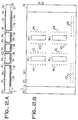
- FIG. 2 shows in Figure 2a a sectional view of a printed card according to the invention and in Figure 2b a top view of this card.
- This card 1 represents a variant of that shown in FIG. 1.
- the heat sink 30 is not coated on its two lateral edges 32, 33 and 34, 35 of the insulating layer 31. The heat sink is thus directly in contact with the thermal slide when the card is connected, both on one side and on the other, the printed circuit 36 stopping before the lateral end of the card.
- This printed circuit 36 also includes interconnection holes 37, 38, 39 and 40 between the different layers which constitute it.
- the printed card 1- also comprises perforations 41, 42, 43, 44 passing through both the heat sink and the printed circuit is intended for the passage of the connections of the electronic components to be fixed on this card.
- connection holes are isolated using the insulating layer 31 in the corresponding areas of the heat sink. This comprises on its outer face, zones 45 and 46 not coated with the insulating layer 31. These zones correspond to the locations of the boxes of electronic components intended to be fixed to this card.
- electrical connection holes 47 and 48 similar to holes such as 41, 42, 43 and 44, and intended to connect the electrical conductors of the printed circuit 36 to the outside of the card, via connectors circuit boards well known to those skilled in the art.
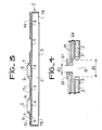
- FIG. 3 shows a variant of the circuit according to the invention, variant of FIG. 1 in which the heat sink has no perforation.
- the thermal drain 2 is covered on its front face with a uniform layer of insulating paste 3 except on the two lateral edges 19 intended to be in thermal contact with the thermal slides as shown in FIG. 1.
- On the upper face of the drain thermal there are the printed circuit 11 and its interconnection holes between layers such as 12, 13 and 14. This interconnection circuit 11 has at the level of components such as 5 openings which also extend into the insulating layer 3 of the heat sink 2.
- connection pads connection pads
- con lateral connections which can be soldered flat on the printed circuits (connections 6 and 7 in FIG. 3)
- thermal seal 4 known per se, which thermally connects the base of the housing 5 to the heat sink 2.
- the heat sink does not need to be perforated since the components do not pass through it, which still allows d 'improving the evacuation of calories due to the continuity of the metal constituting the heat sink.
- the protective layer 3 located on the back of the heat sink is not necessary in the present case and it can possibly be eliminated so as to bring, for example, a convection cooling radiator over the whole of the lower part of the heat sink 2. It can also be seen that the zones 19 of the heat sink not provided with insulating layers 3 are located in the case shown in FIG. 3 on the back of the heat sink.
- FIG. 4 represents a partial view of a connection hole according to a preferred variant of the invention.
- the same elements as those in Figure 1 have the same references.
- the opening made in the heat sink has a width d 1 greater than the opening for the passage of the connection of the component and its soldering on the printed circuit 11 which has a width d 2 between the two ends of the added pad 61.
- the adhesive layer 60 clearly highlighted between the printed circuit 11 and the heat sink 2 covered with its insulating layer 3.
- a metal support 1 mm thick is then drilled in the same way as drilling the connection holes of components of the multi-layer printed circuit.
- This metallic core is made of aluminum or its alloys, copper, steel, ferro-nickel, titanium with a coefficient of expansion compatible with that of ceramics. It is then fitted with spares or areas spared at the locations corresponding to the housing of the electronic components which will be placed on the card as well as on the two opposite lateral edges corresponding to the thermal connection.
- This metal substrate is then immersed in a fluidized bed of epoxy resin, the resin coming to be distributed uniformly over the entire metal plate.
- the metal substrate is then removed from this fluidized bed and the resin is then cut at the locations identified by the covers, after passing through an oven so as to crosslink or harden the epoxy resin, thus producing a uniform surface insulating layer on the entire heat sink including in the connection holes.
- This method of depositing insulating layers and their implementation are given for example in French patent 2,386,959. It is also possible to proceed by electrostatic deposition of paint through masks protecting the parts situated under the components and the borders. of the card so as to directly produce the appropriate insulating layer.
- the multi-layer printed circuit and the heat sink thus coated with its insulating layer are then laminated using an epoxy adhesive for example.
- an epoxy adhesive for example.
Abstract
Description
La présente invention concerne une carte imprimée électrique et thermique, un procédé de fabrication d'une telle carte ainsi qu'un système d'interconnexion thermique et électrique utilisant cette carte.The present invention relates to an electrical and thermal printed board, a method of manufacturing such a board and a thermal and electrical interconnection system using this board.
Les problèmes de dissipation thermique se posent notamment dans les appareils ou équipements comportant un grand nombre de cartes imprimées munies de composants électroniques. Parmi ces composants, certains d'entre eux dissipent une quantité de chaleur importante qu'il convient d'évacuer dans les meilleures conditions possibles afin de maintenir lesdits composants dans des conditions de fonctionnement acceptables.The problems of heat dissipation arise in particular in apparatus or equipment comprising a large number of printed cards provided with electronic components. Among these components, some of them dissipate a significant amount of heat which must be removed under the best possible conditions in order to maintain said components in acceptable operating conditions.
La carte imprimée selon l'invention est caractérisée en ce qu'elle comporte, solidaire l'un de l'autre, un circuit imprimé mono ou multi-couches et un drain thermique constitué d'une âme métallique revêtue de résine isolante, le circuit imprimé et le drain thermique comportant une pluralité de trous de connexion respectivement alignés deux par deux, lesdits trous du drain thermique étant également revêtus de résine isolante, le drain thermique comportant en outre des zones non revêtues de résine isolante disposée sur la face extérieure de celui-ci. Ces zones non revêtues de résine isolante seront d'une part au moins une bordure de la carte imprimée, et d'autre part les emplacements prévus pour les composants électroniques dissipant de la chaleur.The printed card according to the invention is characterized in that it comprises, integral with one another, a single or multi-layer printed circuit and a heat sink consisting of a metal core coated with insulating resin, the circuit printed and the heat sink comprising a plurality of connection holes respectively aligned two by two, said holes of the heat drain also being coated with insulating resin, the heat drain further comprising areas not coated with insulating resin arranged on the outside of that -this. These areas not coated with insulating resin will be on the one hand at least one border of the printed card, and on the other hand the locations provided for the heat-dissipating electronic components.
De cette manière, en effet, on constate que la carte imprimée ainsi réalisée outre le fait que le drain thermique généralement métallique contribue à rigidifier le circuit imprimé qui peut être très mince, permet alors une dissipation thermique correcte des composants électroniques, dissipation effectuée par conduction. En effet, chaque composant électronique, dissipant de la chaleur, est placé en un endroit de la carte comportant une partie non revêtue de résine isolante ce qui permet de mettre en contact thermique étroit le boîtier dudit composant et le drain thermique. Au besoin, pour améliorer la conduction thermique, on interpose entre les deux une pâte de conduction thermique bien connue de l'homme de métier ayant un coefficient de conduction thermique supérieure à celui de l'air. Les calories ainsi dissipées par le composant électronique et transmises à son boîtier sont alors drainées par lè drain thermique jusque sur les bords latéraux de la carte qui comporte des bandes latérales non revêtues de résine isolante. Ces bandes latérales sont insérées dans des connecteurs thermiques réalisés sous forme de glissières dans lesquelles viennent se bloquer les extrémités de la carte en contact étroit avec lesdites glissières éventuellement traversées par un liquide de refroidissement.In this way, in fact, it can be seen that the printed card thus produced, in addition to the fact that the generally metallic thermal drain contributes to stiffening the printed circuit which can be very thin, then allows correct heat dissipation of the electronic components, dissipation carried out by conduction. Indeed, each electronic component, dissipating heat, is placed in a location on the card comprising a part not coated with insulating resin, which makes it possible to place the housing of said component and the heat sink in close thermal contact. If necessary, to improve the thermal conduction, a thermal conduction paste well known to those skilled in the art is interposed between the two having a coefficient of thermal conduction greater than that of air. The calories thus dissipated by the electronic component and transmitted to its casing are then drained by the heat sink as far as the lateral edges of the card which has lateral strips not coated with insulating resin. These lateral strips are inserted in thermal connectors produced in the form of slides in which the ends of the card come into contact in close contact with said slides possibly crossed by a coolant.
Une telle structure de carte et de système d'interconnexion telle que décrit ci-dessus permet d'améliorer considérablement l'évacuation des calories dissipées par ses composants et permet ainsi une plus grande densité de carte à l'intérieur d'un même équipement électrique.Such a card and interconnection system structure as described above makes it possible to considerably improve the evacuation of the calories dissipated by its components and thus allows a greater density of cards inside the same electrical equipment. .
L'invention concerne également un procédé de fabrication d'une carte imprimée telle que décrit ci-dessus. Sans entrer dans les détails auxquels on pourra se reporter ci-après, ce procédé est essentiellement remarquable en ce que le drain thermique, généralement une plaque métallique, est percé tout d'abord de trous de connexion à travers lesquels passeront les connexions des composants de la carte. Ce perçage s'effectue en pratique à l'aide de la même bande de commande de la machine outil de perçage que le circuit imprimé qui lui est associé. Après perçage, on dépose sur le drain thermique aux endroits voulus des caches du type ruban adhésif de manière à repérer ces endroits. Une peinture isolante est ensuite déposée uniformément sur l'ensemble du drain y compris dans les trous. Ce dépôt s'effectue soit par la technique de peinture électrostatique, soit par la technique du lit fluidisé (voir pour plus de détail sur ces techniques employés dans le domaine des circuits imprimés le brevet français 2 386 959). Après polymérisation de la résine (généralement une résine époxy), le drain thermique est ainsi isolé uniformément. On retire alors les caches aux endroits où ils avaient été disposés mettant ainsi des zones à nu sur le drain thermique. Le circuit imprimé correspondant est ensuite réalisé et assemblé avec ce drain thermique de manière connue en soi, soit par contre-collage d'un circuit imprimé mono ou multi-couches réalisé sur tissu de verre époxy par exemple, soit par des techniques additives ou soustractives de dépôt métallique sur la résine isolante déposée sur le drain thermique. Suivant les cas, comme on le verra plus loin, l'étape de perçage du circuit imprimé peut être évitée, tandis que le circuit imprimé comporte alors des fenêtres qui viennent en coïncidence avec les zones mises à nu du drain thermique. Ces zones sont traitées ensuite pour être protégées contre l'oxydation, de manière connue en soi.The invention also relates to a method of manufacturing a printed card as described above. Without going into the details to which reference may be made below, this process is essentially remarkable in that the heat sink, generally a metal plate, is pierced first of all with connection holes through which the connections of the components of the the map. This drilling is carried out in practice using the same control strip of the drilling machine tool as the printed circuit associated with it. After drilling, place on the heat sink at the desired locations masks of the adhesive tape type so as to identify these locations. An insulating paint is then deposited uniformly over the entire drain including in the holes. This deposit is made either by the painting technique electrostatic, or by the fluidized bed technique (see for more details on these techniques used in the field of printed circuits the French patent 2,386,959). After polymerization of the resin (generally an epoxy resin), the heat sink is thus insulated uniformly. The covers are then removed from the places where they had been placed, thus exposing exposed areas on the heat sink. The corresponding printed circuit is then produced and assembled with this heat sink in a manner known per se, either by laminating a mono or multi-layer printed circuit produced on epoxy glass fabric for example, or by additive or subtractive techniques metallic deposit on the insulating resin deposited on the heat sink. Depending on the case, as will be seen below, the step of drilling the printed circuit can be avoided, while the printed circuit then includes windows which come into coincidence with the exposed areas of the heat sink. These areas are then treated to be protected against oxidation, in a manner known per se.
L'invention concerne également un système d'interconnexion thermique et électrique de composants électroniques dissipant de la chaleur, système utilisant une carte telle que décrite ci-dessus. La carte revêtue de composants électroniques aux endroits adéquats est disposée de préférence entre deux connecteurs thermiques sous forme de glissières situées de part et d'autre de la carte, tandis que la connexion électrique de la carte avec l'appareillage extérieur peut s'effectuer à l'aide de connecteurs électriques disposés sur l'un ou les deux autres bords de la carte. Bien entendu, les connecteurs thermiques utilisés peuvent être du type connecteurs électriques et thermiques tels que décrits dans le brevet français 2 471 059. Dans ce cas, les pistes de la carte imprimée sont en contact électrique avec les contacts de la glissière thermique, isolés entre eux de manière adéquate.The invention also relates to a system for the thermal and electrical interconnection of heat-dissipating electronic components, a system using a card as described above. The card coated with electronic components in the appropriate places is preferably placed between two thermal connectors in the form of slides located on either side of the card, while the electrical connection of the card with the external equipment can be made using electrical connectors on one or both of the other edges of the card. Of course, the thermal connectors used can be of the electrical and thermal connector type as described in French patent 2,471,059. In this case, the tracks of the circuit board are in electrical contact with the contacts of the thermal slide, isolated between them adequately.
Dans toute la suite de l'exposé, le terme drain thermique désigne tout type de support métallique et/ou fibreux capable de conduire la chaleur. Ce support est également conducteur électrique, nécessitant, par conséquent, une isolation électrique en particulier des trous dans lesquels passent les pattes des composants.Throughout the rest of the description, the term thermal drain designates any type of metallic and / or fibrous support capable of conducting heat. This support is also electrically conductive stick, therefore requiring electrical insulation, in particular holes through which the legs of the components pass.
L'invention sera mieux comprise à l'aide des exemples de réalisation suivants, donnés à titre non limitatif, conjointement avec les figures qui représentent :
- - la figure 1, une vue partielle en coupe d'un système d'interconnexion utilisant une carte imprimée selon l'invention,
- - la figure 2, une vue en coupe et une vue de dessus correspondantes d'une carte selon l'invention,
- - la figure 3, une variante de la carte selon l'invention dans laquelle le drain thermique n'a aucune perforation,
- - la figure 4, une vue partielle d'un trou de connexion selon une variante préférentielle.
- FIG. 1, a partial sectional view of an interconnection system using a printed card according to the invention,
- FIG. 2, a sectional view and a corresponding top view of a card according to the invention,
- FIG. 3, a variant of the card according to the invention in which the heat sink has no perforation,
- - Figure 4, a partial view of a connection hole according to a preferred embodiment.
Sur la figure 1, est représentée une vue en coupe d'un système d'interconnexion électrique et thermique selon l'invention. La carte imprimée 1 selon l'invention est constituée d'un drain thermique métallique 2 sur lequel est déposée une couche isolante 3 telle qu'une résine époxy par exemple. Un circuit imprimé 11 muni de trous d'interconnexion entre couches telles que 12, 13, 14, etc... est rendu solidaire du drain thermique 2 sur la partie inférieure de celui-ci. La couche isolante 3 sépare du drain 2 des couches conductrices du circuit imprimé 11. Des trous de connexion 8 et 9 de composants tels que 5 traversent le drain thermique 2 et le circuit imprimé 11. Les pattes de connexion telles que 6 et 7 du composant 5 traversent ainsi ces trous revêtus intérieurement au niveau du drain thermique 2 de la couche isolante 3, lesdites pattes de connexion étant reliées en 15 et 16 au circuit imprimé 11. Sous le boîtier 5 du composant électronique, se trouve une partie 4 du drain thermique 2 non recouverte de la couche isolante 3, réalisant ainsi une ouverture dans cette couche isolante 3 qui recouvre par ailleurs le drain thermique 2. Pour améliorer la conduction thermique entre le boîtier 5 et le drain thermique 2, on peut incorporer dans cette ouverture 4 une pâte conductrice connue en soi ayant une bonne conduction thermique. Sur l'extrémité supérieure gauche de la carte 1, la couche isolante 3 est interrompue mettant a nue ainsi une partie 19 du drain thermique 2 non revêtue de cette couche isolante. Cette partie 19 est au contact de la paroi 10 correspondante de la glissière thermique dans laquelle vient s'enficher l'extrémité de la carte. Le contact thermique est maintenu contre celle-ci à l'aide du contact presseur 18 maintenu en pression par la rotation de la came 17. L'extrémité du drain thermique 2 revêtue de la couche isolante 3 vient ici en butée contre le fond 20 de la rainure de la glissière thermique. On constate ici que le circuit imprimé 11 s'étend jusqu'à l'extrémité du drain thermique 2, séparée de celui-ci par la couche isolante 3. Cette figure illustre l'originalité du système d'interconnexion thermique selon l'invention dans lequel le composant 5 dissipant de la chaleur est placé côté drain thermique dans une ouverture du revêtement isolant 3 de celui-ci (meilleure conduction) tandis que ses connexions 6 et 7 traversent le drain dans des trous 8 et 9, isolés par le revêtement 3 également et puis traversent les trous correspondants sur le circuit imprimé sur la couche conductrice inférieure duquel elles sont fixées par les brasures 15 et 16. Ce dernier peut être, bien entendu, du type multi-couche, avec des pistes conductrices disposées côté drain thermique 2. De toutes manières, même lorsque ce dernier est conducteur électrique (comme l'aluminium), le revêtement isolant 3 qui recouvre tout le drain sauf aux endroits voulus, isole électriquement le drain thermique et les pistes du circuit imprimé. Les calories engendrées par le circuit 5 sont donc drainées par conduction vers la glissière thermique, via le drain thermique 2, la glissière thermique évacuant ensuite les calories de manière connue en soi vers l'extérieur du système.In Figure 1 is shown a sectional view of an electrical and thermal interconnection system according to the invention. The printed
La figure 2 représente sur la figure 2a une vue en coupe d'une carte imprimée selon l'invention et sur la figure 2b une vue de dessus de cette carte. Cette carte 1 représente une variante de celle représentée sur la figure 1. En effet, sur cette figure 2, le drain thermique 30 n'est pas revêtu sur ses deux bordures latérales 32, 33 et 34, 35 de la couche isolante 31. Le drain thermique est ainsi directement au contact de la glissière thermique lorsque la carte est connectée, aussi bien sur une face que sur l'autre, le circuit imprimé 36 s'arrêtant avant l'extrémité latérale de la carte. Ce circuit imprimé 36 comporte également des trous d'interconnexion 37, 38, 39 et 40 entre les différentes couches qui le constituent. La carte imprimée 1- comporte par ailleurs des perforations 41, 42, 43, 44 traversant à la fois le drain thermique et le circuit imprimé est destiné au passage des connexions des composants électroniques à fixer sur cette carte. Ces trous de connexion sont isolés à l'aide de la couche isolante 31 dans les zones correspondantes du drain thermique. Celui-ci comporte sur sa face extérieure, des zones 45 et 46 non revêtues de la couche isolante 31. Ces zones correspondent aux emplacements des boîtiers de composants électroniques destinés à être fixés sur cette carte. On remarque par ailleurs des trous de connexion électrique 47 et 48 semblables aux trous tels que 41, 42, 43 et 44, et destinés à relier les conducteurs électriques du circuit imprimé 36 à l'extérieur de la carte, par l'intermédiaire de connecteurs de circuit imprimé bien connus de l'homme de métier.2 shows in Figure 2a a sectional view of a printed card according to the invention and in Figure 2b a top view of this card. This
Sur la figure 3, est représentée une variante du circuit selon l'invention, variante de la figure 1 dans laquelle le drain thermique ne comporte aucune perforation. Sur cette figure, les mêmes éléments que ceux de la figure 1 portent les mêmes références. Le drain thermique 2 est recouvert sur sa face antérieure d'une couche uniforme de pâte isolante 3 sauf sur les deux bords latéraux 19 destinés à être en contact thermique avec les glissières thermiques telles que représentées sur la figure 1. Sur la face supérieure du drain thermique, se trouvent le circuit imprimé 11 et ses trous d'interconnexion entre couches telles que 12, 13 et 14. Ce circuit d'interconnexion 11 comporte au niveau des composants tels que 5 des ouvertures qui se prolongent également dans la couche isolante 3 du drain thermique 2. Les composants 5 qui sont du type par report à plat, c'est-à-dire munis soit de plots de connexions, soit de connexions latérales pouvant être soudées à plat sur les circuits imprimés (connexions 6 et 7 sur la figure 3), sont alors fixés sur le circuit imprimé 11 dans l'ouverture correspondante, cette ouverture étant munie sur sa partie inférieure d'un joint thermique 4 connu en soi, qui relie thermiquement la base du boîtier 5 au drain thermique 2. On constate dans cette variante que le drain thermique n'a pas besoin d'être perforé puisque les composants ne traversent pas celui-ci, ce qui permet encore d'améliorer l'évacuation des calories du fait de la continuité du métal constituant le drain thermique. On peut noter par ailleurs que la couche de protection 3 située au dos du drain thermique n'est pas nécessaire dans le cas présent et elle peut éventuellement être supprimée de manière à rapporter par exemple un radiateur de refroidissement par convection sur l'ensemble de la partie inférieure du drain thermique 2. On constate également que les zones 19 du drain thermique non pourvues de couches isolantes 3 sont situées dans le cas représenté sur la figure 3 au dos du drain thermique.FIG. 3 shows a variant of the circuit according to the invention, variant of FIG. 1 in which the heat sink has no perforation. In this figure, the same elements as those in Figure 1 have the same references. The
La figure 4 représente une vue partielle d'un trou de connexion selon une variante préférentielle de l'invention. Sur cette figure, les mêmes éléments que ceux de la figure 1 portent les mêmes références. Dans cette variante correspondant à la structure de la figure 1, l'ouverture réalisée dans le drain thermique a une largeur d1 supérieure à l'ouverture pour le passage de la connexion du composant et sa soudure sur le circuit imprimé 11 qui a une largeur d2 entre les deux extrémités de la pastille rapportée 61. Ceci permet une utilisation du circuit selon l'invention pour tous les types de boîtiers en particulier pour ceux qui présentent un épaulement au niveau des pattes de connexion évitant ainsi un contact des pattes avec la couche isolante 3 au moment de l'insertion. On notera également sur cette figure la couche d'adhésif 60 nettement mise en évidence entre le circuit imprimé 11 et le drain thermique 2 recouvert de sa couche isolante 3.FIG. 4 represents a partial view of a connection hole according to a preferred variant of the invention. In this figure, the same elements as those in Figure 1 have the same references. In this variant corresponding to the structure of FIG. 1, the opening made in the heat sink has a width d 1 greater than the opening for the passage of the connection of the component and its soldering on the printed
EXEMPLE :
- On réalise un circuit imprimé doubles faces ou multi-couches en stratifié verre époxy mince selon la technique bien connue.
- A double-sided or multi-layer printed circuit is produced in thin epoxy glass laminate according to the well-known technique.
Un support métallique d'épaisseur 1 mm est ensuite percé de la même manière que le perçage des trous de connexion de composants du circuit imprimé multi-couches. Cette âme métallique est en aluminium ou ses alliages, cuivre, acier, ferro-nickel, titane avec un coefficient de dilatation compatible avec celui des céramiques. Elle est ensuite munie de caches ou zones épargnes aux endroits correspondant au boîtier des composants électroniques qui seront placés sur la carte ainsi que sur les deux bordures latérales opposées correspondant à la connexion thermique. Ce substrat métallique est ensuite plongé dans un lit fluidisé de résine époxy, la résine venant se disposer uniformément sur toute la plaque métallique. Le substrat métallique est alors retiré de ce lit fluidisé et l'on découpe ensuite la résine aux endroits repérés par les caches, après passage dans un four de manière à réaliser une réticulation ou durcissement de la résine époxy réalisant ainsi une couche isolante superficielle uniforme sur l'ensemble du drain thermique y compris dans les trous de connexion. Des détails sur ce procédé de dépôt de couches isolantes et leur mise en oeuvre sont donnés par exemple dans le brevet français 2 386 959. On pourra également procéder par dépôt électrostatique de peinture à travers des masques protégeant les parties situées sous les composants et les bordures de la carte de manière à réaliser directement la couche isolante adéquate.A
Le circuit imprimé multi-couches et le drain thermique ainsi revêtus de sa couche isolante sont ensuite contre-collés à l'aide d'une colle époxy par exemple. On peut également utiliser un circuit imprimé sur verre époxy du type pré-impégné à l'aide d'une résine époxy pré-polymère, le passage en température de l'ensemble drain thermique et circuit imprimé réalisant la solidarisation de ces deux éléments.The multi-layer printed circuit and the heat sink thus coated with its insulating layer are then laminated using an epoxy adhesive for example. One can also use a printed circuit on epoxy glass of the pre-impregnated type using a pre-polymer epoxy resin, the temperature rise of the heat sink and printed circuit assembly securing these two elements.
Claims (10)
Applications Claiming Priority (2)
| Application Number | Priority Date | Filing Date | Title |
|---|---|---|---|
| FR8205253A FR2524250A1 (en) | 1982-03-26 | 1982-03-26 | ELECTRICAL AND THERMAL PRINTED CARD, METHOD FOR MANUFACTURING SUCH A CARD, AND THERMAL AND ELECTRICAL INTERCONNECTION SYSTEM USING SUCH A CARD |
| FR8205253 | 1982-03-26 |
Publications (1)
| Publication Number | Publication Date |
|---|---|
| EP0090727A1 true EP0090727A1 (en) | 1983-10-05 |
Family
ID=9272461
Family Applications (1)
| Application Number | Title | Priority Date | Filing Date |
|---|---|---|---|
| EP83400603A Withdrawn EP0090727A1 (en) | 1982-03-26 | 1983-03-23 | Electrically and thermally printed circuit board, process for making such a board and interconnection system utilizing such a board |
Country Status (2)
| Country | Link |
|---|---|
| EP (1) | EP0090727A1 (en) |
| FR (1) | FR2524250A1 (en) |
Cited By (4)
| Publication number | Priority date | Publication date | Assignee | Title |
|---|---|---|---|---|
| US4536824A (en) * | 1983-03-28 | 1985-08-20 | Goodyear Aerospace Corporation | Indirect cooling of electronic circuits |
| FR2579060A1 (en) * | 1985-03-18 | 1986-09-19 | Socapex | THERMAL EXCHANGER PRINTED CIRCUIT BOARD AND METHOD OF MANUFACTURING SUCH A CARD |
| US4675784A (en) * | 1983-12-13 | 1987-06-23 | Rolf Dahlberg | Printed circuit board |
| FR3080971A1 (en) * | 2018-05-07 | 2019-11-08 | Continental Automotive France | CIRCUIT BOARD PRINTED WITH A THERMAL DISSIPATOR FOR A POWER SOLIDARIZED POWER MODULE |
Families Citing this family (1)
| Publication number | Priority date | Publication date | Assignee | Title |
|---|---|---|---|---|
| US4996629A (en) * | 1988-11-14 | 1991-02-26 | International Business Machines Corporation | Circuit board with self-supporting connection between sides |
Citations (4)
| Publication number | Priority date | Publication date | Assignee | Title |
|---|---|---|---|---|
| DE1965851A1 (en) * | 1968-12-30 | 1970-07-02 | Gen Motors Corp | Thermally conductive holder for a printed circuit board |
| DE2743647A1 (en) * | 1977-09-28 | 1979-03-29 | Siemens Ag | Component cooling in communication and measurement equipment - uses metal plate coated with insulating foil which carries components and printed circuit |
| FR2423953A1 (en) * | 1978-04-18 | 1979-11-16 | Radiotechnique Compelec | Multilayer printed circuit - comprising network and insulating layers, with through hole contacts formed with metallised walls surrounded by insulating plastics |
| EP0006810A1 (en) * | 1978-06-29 | 1980-01-09 | L.C.C.-C.I.C.E. - Compagnie Europeenne De Composants Electroniques | Method of producing an integrated hybrid circuit |
-
1982
- 1982-03-26 FR FR8205253A patent/FR2524250A1/en active Granted
-
1983
- 1983-03-23 EP EP83400603A patent/EP0090727A1/en not_active Withdrawn
Patent Citations (4)
| Publication number | Priority date | Publication date | Assignee | Title |
|---|---|---|---|---|
| DE1965851A1 (en) * | 1968-12-30 | 1970-07-02 | Gen Motors Corp | Thermally conductive holder for a printed circuit board |
| DE2743647A1 (en) * | 1977-09-28 | 1979-03-29 | Siemens Ag | Component cooling in communication and measurement equipment - uses metal plate coated with insulating foil which carries components and printed circuit |
| FR2423953A1 (en) * | 1978-04-18 | 1979-11-16 | Radiotechnique Compelec | Multilayer printed circuit - comprising network and insulating layers, with through hole contacts formed with metallised walls surrounded by insulating plastics |
| EP0006810A1 (en) * | 1978-06-29 | 1980-01-09 | L.C.C.-C.I.C.E. - Compagnie Europeenne De Composants Electroniques | Method of producing an integrated hybrid circuit |
Non-Patent Citations (1)
| Title |
|---|
| MACHINE DESIGN, vol. 48, no. 9, avril 1976, page 36, Cleveland, USA * |
Cited By (7)
| Publication number | Priority date | Publication date | Assignee | Title |
|---|---|---|---|---|
| US4536824A (en) * | 1983-03-28 | 1985-08-20 | Goodyear Aerospace Corporation | Indirect cooling of electronic circuits |
| US4675784A (en) * | 1983-12-13 | 1987-06-23 | Rolf Dahlberg | Printed circuit board |
| EP0164392B1 (en) * | 1983-12-13 | 1988-12-07 | DAHLBERG, Rolf | Printed circuit board |
| FR2579060A1 (en) * | 1985-03-18 | 1986-09-19 | Socapex | THERMAL EXCHANGER PRINTED CIRCUIT BOARD AND METHOD OF MANUFACTURING SUCH A CARD |
| EP0197817A1 (en) * | 1985-03-18 | 1986-10-15 | Socapex | Printed-circuit board with a heat exchanger, and process for manufacturing it |
| US4706164A (en) * | 1985-03-18 | 1987-11-10 | Amphenol Corporation | Printed circuit card with heat exchanger and method for making such a card |
| FR3080971A1 (en) * | 2018-05-07 | 2019-11-08 | Continental Automotive France | CIRCUIT BOARD PRINTED WITH A THERMAL DISSIPATOR FOR A POWER SOLIDARIZED POWER MODULE |
Also Published As
| Publication number | Publication date |
|---|---|
| FR2524250A1 (en) | 1983-09-30 |
| FR2524250B1 (en) | 1985-03-08 |
Similar Documents
| Publication | Publication Date | Title |
|---|---|---|
| EP0308296B1 (en) | Printed circuit comprising a heat sink | |
| FR2688629A1 (en) | Method and device for three-dimensional encapsulation of semiconductor chips | |
| FR2763467A1 (en) | STRUCTURE FOR CONNECTING ELECTRICAL COMPONENTS TO A CENTRAL UNIT | |
| EP0490739A1 (en) | Interconnection method and device for three-dimensional integrated circuits | |
| FR2560731A1 (en) | Thermally conducting multilayer printed card | |
| FR2735648A1 (en) | COOLING METHOD OF AN INTEGRATED CIRCUIT MOUNTED IN A HOUSING | |
| EP1550361B1 (en) | Three-dimensional electronic module | |
| EP0044247B1 (en) | Method of producing a carrier for electronic components for the interconnection of integrated-circuit chips | |
| FR2589031A1 (en) | ARRANGEMENT OF CIRCUIT ELEMENT GROUPS SUPPORTING ELECTRICAL AND COOLING COMPONENTS | |
| EP0090727A1 (en) | Electrically and thermally printed circuit board, process for making such a board and interconnection system utilizing such a board | |
| EP0233674A1 (en) | Information bus connector | |
| FR2675632A1 (en) | Packaging device for integrated circuits | |
| EP0124428A1 (en) | Lighter mounting for electronic components | |
| EP1054445A1 (en) | Electronic package on circuit board and its manufacture | |
| EP0085622B1 (en) | Mounting support for integrated circuit-housing with external leads formed around the housing perimeter | |
| EP0083265B1 (en) | Interconnection carrier on a printed circuit for an integrated-circuit housing, and interconnection system utilizing such a carrier | |
| FR2764414A1 (en) | NON-CONTACT CHIP CARD MANUFACTURING PROCESS | |
| WO2014198688A1 (en) | Cooled printed circuit with multi-layer structure and low dielectric losses | |
| FR2706730A1 (en) | Power electronics module having a heat-sink support | |
| WO1998008363A1 (en) | Method for manufacturing a device for burning off thermal energy produced by electronic components embedded in a printed circuit card, and resulting device | |
| FR2551618A1 (en) | Process for manufacturing a printed circuit having buried layers and printed circuit obtained by such a process. | |
| EP0163581B1 (en) | Production method and device for electrical connections between two printed-circuit boards, and electrical connection method using the device | |
| FR2764473A1 (en) | ELECTRONIC DRAWER COMPRISING AN IMPROVED HEAT EXHAUST DEVICE | |
| FR2699039A1 (en) | Multilayer circuit board for use in electronics applications - has circuit board separated by isolating layers with integrated circuits mounted on lower and upper face | |
| EP1036489B1 (en) | Method for surface mounting of a microwave package on a printed circuit and package and printed circuit for implementing said method |
Legal Events
| Date | Code | Title | Description |
|---|---|---|---|
| PUAI | Public reference made under article 153(3) epc to a published international application that has entered the european phase |
Free format text: ORIGINAL CODE: 0009012 |
|
| AK | Designated contracting states |
Designated state(s): DE GB IT Kind code of ref document: A1 Designated state(s): DE GB IT |
|
| 17P | Request for examination filed |
Effective date: 19831103 |
|
| STAA | Information on the status of an ep patent application or granted ep patent |
Free format text: STATUS: THE APPLICATION IS DEEMED TO BE WITHDRAWN |
|
| 18D | Application deemed to be withdrawn |
Effective date: 19850917 |
|
| RIN1 | Information on inventor provided before grant (corrected) |
Inventor name: OLIVE, JEAN-LOUIS Inventor name: BRICAUD, HERVE |