EP0086183B1 - Elektronischer Verstärker für externe Leitung - Google Patents
Elektronischer Verstärker für externe Leitung Download PDFInfo
- Publication number
- EP0086183B1 EP0086183B1 EP83850017A EP83850017A EP0086183B1 EP 0086183 B1 EP0086183 B1 EP 0086183B1 EP 83850017 A EP83850017 A EP 83850017A EP 83850017 A EP83850017 A EP 83850017A EP 0086183 B1 EP0086183 B1 EP 0086183B1
- Authority
- EP
- European Patent Office
- Prior art keywords
- wire side
- optocoupler
- voltage
- circuit
- wire
- Prior art date
- Legal status (The legal status is an assumption and is not a legal conclusion. Google has not performed a legal analysis and makes no representation as to the accuracy of the status listed.)
- Expired
Links
- 230000015556 catabolic process Effects 0.000 claims abstract description 7
- 238000006731 degradation reaction Methods 0.000 claims abstract description 7
- 238000001914 filtration Methods 0.000 claims abstract description 3
- 238000002955 isolation Methods 0.000 claims description 5
- 230000008878 coupling Effects 0.000 description 5
- 238000010168 coupling process Methods 0.000 description 5
- 238000005859 coupling reaction Methods 0.000 description 5
- 230000005540 biological transmission Effects 0.000 description 2
- 239000003990 capacitor Substances 0.000 description 2
- 238000010586 diagram Methods 0.000 description 2
- 230000001681 protective effect Effects 0.000 description 2
- 230000032683 aging Effects 0.000 description 1
- 230000003247 decreasing effect Effects 0.000 description 1
- 230000010354 integration Effects 0.000 description 1
- 230000003287 optical effect Effects 0.000 description 1
- 239000007787 solid Substances 0.000 description 1
Images
Classifications
-
- H—ELECTRICITY
- H04—ELECTRIC COMMUNICATION TECHNIQUE
- H04M—TELEPHONIC COMMUNICATION
- H04M19/00—Current supply arrangements for telephone systems
- H04M19/001—Current supply source at the exchanger providing current to substations
- H04M19/005—Feeding arrangements without the use of line transformers
-
- H—ELECTRICITY
- H04—ELECTRIC COMMUNICATION TECHNIQUE
- H04B—TRANSMISSION
- H04B1/00—Details of transmission systems, not covered by a single one of groups H04B3/00 - H04B13/00; Details of transmission systems not characterised by the medium used for transmission
- H04B1/38—Transceivers, i.e. devices in which transmitter and receiver form a structural unit and in which at least one part is used for functions of transmitting and receiving
- H04B1/40—Circuits
- H04B1/54—Circuits using the same frequency for two directions of communication
- H04B1/58—Hybrid arrangements, i.e. arrangements for transition from single-path two-direction transmission to single-direction transmission on each of two paths or vice versa
- H04B1/587—Hybrid arrangements, i.e. arrangements for transition from single-path two-direction transmission to single-direction transmission on each of two paths or vice versa using opto-couplers
Definitions
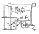
- the present invention relates to an electronic external line repeater containing optocouplers with a two-wire side (two-wire input/output) and an incoming and outgoing four-wire side.
- a repeater is used for connecting a two-wire central line to a subscriber exchange.
- the object of the present invention is to provide an external line repeater containing optocouplers (LED and phototransistor) arranged between the incoming two-wire side and the four-wire sides of the repeater, a self-compensating reverse feed-back being incorporated in the repeater for counteracting initial spread and age degradation of the optocoupler.
- optocouplers LED and phototransistor
- the left-hand end terminal constitutes the two-wire side, across which a voltage U, appears, in its turn constituting an outgoing or incoming speech signal plus a DC component for supplying current to the repeater.
- the resistors R1 and R2 are two protective resistors, and the circuit D is an overvoltage protection known per se.
- Both inputs of a differential amplifier circuit F1 are connected across the two-wire side and across the other side of the protective resistors, for obtaining an output signal u 3 , which is the difference signal between the voltages U, and U 2 and is solely the speech signal. This is taken via a buffer stage F5 to an outgoing four-wire side formed by the output of the buffer stage F5.
- the input stage of the differential amplifier circuit F1 input step consists of an operational amplifier with a high input impedance, the circuit F1 (and the following stages) thus not loading the two-wire side.
- the incoming four-wire side is formed by a buffer stage F6 comprising (as with the buffer stage F5) an operational amplifier ' circuit of known embodiment.
- a feed-back loop is formed by the circuit F1 and a resistor R to a line amplifier circuit F2 to achieve the desired AC impedance, seen from the two-wire side. This feed-back loop is described in the Swedish Patent Application No. 8200741-0 and is no subject of this invention.
- the line amplifier circuit F2 primarily has the task of receiving the speech signal from the four-wire side (the buffer stage F6) and converting it into a current, which, via the optocoupler, gives a transversal speech voltage across the two-wire side.
- the circuit F2 includes an operational amplifier OP3, the minus input of which forms a first input via a resistor R9 and, via a resistor R10 and a capacitor C 2 , a plus input forming a second input in the line amplifier circuit.
- the output of the amplifier OP3 is connected via a resistor R14 to a LED D2, optically coupled to a photoresistor FT2.
- the operational amplifier OP3 is together with the resistor R14 connected as a voltage-current converter and converts the speech component u o of the output voltage U o at the corresponding speech current i o .
- the bias current I to the LED is obtained by the voltage-current convertion of the DC component in the output voltage U o .
- the diode D2 and phototransistor FT2 constitute a unit and cannot withstand high voltages but is linear within a given working range.
- An example of such an optocoupler is the General Electric H11F1 which works linearly at a suitably selected working point determined by a given bias current I, i.e.
- a second optocoupler comprises the LED D1 and the phototransistor FT1, the latter being connected in series with the phototransistor FT2.
- This optocoupler is not linear but withstands the high voltages which can occur, e.g. those occurring in connecting ringing signals to the repeater.
- the resistors R15 and R16 connected across the phototransistor FT2 and to one terminal (via the resistor R2) of the two-wire side, determine the working point for an output drive stage T1, T2. Furthermore, the resistor R15 protects the phototransistor FT2 against high voltages.
- a lowpass filtering and comparing circuit block F3 is arranged, the input being connected to the output of the drive stage T1, T2, i.e. to the collector-emitter output of the transistor T2.
- the output of the circuit F3 is directly connected to the first input of the circuit F2.
- the block F3 contains an integrating circuit consisting of an operational amplifier OP1, the input resistors R3, R4 and the resistor-capacitor link R5, C1.
- the integrating circuit senses the output voltage U 2 from the drive stage T1, T2, said voltage containing a DC component and an AC component (the speech signal).
- a voltage is thus obtained across the amplifier OP1 which is the voltage U 2 integrated over a given time interval. Since the speech component varies about the DC component of U 2 , this component will at mean be zero on integration, and a lowpass filtered signal U4 is obtained from the voltage U 2 .
- the block F3 further contains an adder circuit comprising the operational amplifier OP2 together with the resistors R6, R7 and R8.
- a further resistor R d is connected between an earthing point and the minus point.
- the resistor R8 is connected to the minus input of the operational amplifier and to the output of the integrating circuit.
- the lowpass filtered output voltage U 4 will increase, resulting in that U 5 will decrease and the DC component I to the input of the LED D2 will increase.
- the LED D2 thus emits more and more photons (the light intensity increases) to the phototransistor FT2, which in turn becomes more and more conductive, the voltage U 2 decreasing.
- the resistors R12 and R18 stabilize the operational amplifier towards an earth potential.
- the block F4 represents a drive stage suitably containing a feedback operational amplifier for the LED D1 included in the high-voltage-resistant optocoupler D1-FT1.
- a signal determining the line state, high- or low-ohmic loop, is applied across the input s, of the block F4.
- the siganl input s is such that the optocoupler D1-FT1 is not activated and the phototransistor FT1 is blocked.
- the diode D1 obtains current and the phototransistor FT1 is conductive, whereby the photocoupler D2-FT2 is activated to connect speech signals from the receiver path of the four-wire side.
- Both optocouplers D1-FT1 and D2-FT2 have a too small coupling factor and drive capacity of the respective output transistor for being able to drive the two-wire loop directly.
- the couplers have been supplemented by the high-voltage-resistant and also linearly operated Dar- lington-type ouptut stage T1, T2. It is of interest to note here that the conduction voltage of the output transistor T2 is low and that the current lowering ability in a conducting state is sufficiently good so that the series impedance during impulsing can be kept low.
Landscapes
- Engineering & Computer Science (AREA)
- Signal Processing (AREA)
- Power Engineering (AREA)
- Computer Networks & Wireless Communication (AREA)
- Amplifiers (AREA)
- Cable Transmission Systems, Equalization Of Radio And Reduction Of Echo (AREA)
- Telephone Function (AREA)
- Burglar Alarm Systems (AREA)
- Liquid Developers In Electrophotography (AREA)
- Telephonic Communication Services (AREA)
- Devices For Supply Of Signal Current (AREA)
- Networks Using Active Elements (AREA)
Claims (1)
- Elektronischer Verstärker für externe Leitung zur Verbindung einer Zwei-Draht-Leitung über eine Vier-Draht-Verbindung an eine Teilnehmervermittlung, die eine Zwei-Draht-Seite und eine eingehende und ausgehende Vier-Draht-Seite umfaßt, wobei zur Isolation zwischen der eingehenden Vier-Draht-Seite und der Zwei-Draht-Seite eine erste und eine zweite Optokopplereinheit (D1-FT1, D2-FT2) mit dazugehörenden Treiberverstärkerstufen (T1, T2) angeordnet ist, wobei die erste Einheit einen hochspannungsfesten Optokoppler (D1-FT1) und die zweite einen Optokoppler (D2-FT2) mit guter Linearität für den Bereich, in dem der Sprachstrom von der, Vier-Draht-Seite zu der Zwei-Draht-Seite variiert, umfaßt gekennzeichnet durch einen selbstkompensierenden negativ rückgekoppelten Schaltkreis, der hochohmig an die Zwei-Draht-Seite angeschlossen ist und der an die zweite Optokopplereinheit (D2-FT2) angeschlossen ist, wobei der Rückkopplungsschaltkreis einen integrierenden und vergleichenden Schaltkreis (F3) für die Tiefpaßfilterung der Spannung (U2), die über der Zwei-Draht-Seite anliegt und für den Vergleich der tiefpaßgefilterten Spannung (U4) mit einer direkten Spannung (Ud), ebenso wie einen addierenden und einen spannung-stromwandelnden Schaltkreis (F2) umfaßt, für die Summierung der Ausgangsspannung (U5) aus dem vergleichenden Schaltkreis und dem eingehenden Signal über der Vier-Draht-Seite und für die Umwandlung der Ausgangsspannung (U5) in einen Vorspannungsstrom (1) durch das lichtemittierende Element (D2) des zweiten Optokopplers, um der Anfangsstreuung und der Alterung des zweiten Optokopplers entgegenzuwirken.
Priority Applications (1)
| Application Number | Priority Date | Filing Date | Title |
|---|---|---|---|
| AT83850017T ATE35074T1 (de) | 1982-02-09 | 1983-01-26 | Elektronischer verstaerker fuer externe leitung. |
Applications Claiming Priority (2)
| Application Number | Priority Date | Filing Date | Title |
|---|---|---|---|
| SE8200740 | 1982-02-09 | ||
| SE8200740A SE430197B (sv) | 1982-02-09 | 1982-02-09 | Elektroniskt externlinjeoverdrag |
Publications (3)
| Publication Number | Publication Date |
|---|---|
| EP0086183A2 EP0086183A2 (de) | 1983-08-17 |
| EP0086183A3 EP0086183A3 (en) | 1984-08-15 |
| EP0086183B1 true EP0086183B1 (de) | 1988-06-08 |
Family
ID=20345949
Family Applications (1)
| Application Number | Title | Priority Date | Filing Date |
|---|---|---|---|
| EP83850017A Expired EP0086183B1 (de) | 1982-02-09 | 1983-01-26 | Elektronischer Verstärker für externe Leitung |
Country Status (6)
| Country | Link |
|---|---|
| US (1) | US4560843A (de) |
| EP (1) | EP0086183B1 (de) |
| AT (1) | ATE35074T1 (de) |
| CA (1) | CA1198844A (de) |
| DE (1) | DE3377044D1 (de) |
| SE (1) | SE430197B (de) |
Families Citing this family (2)
| Publication number | Priority date | Publication date | Assignee | Title |
|---|---|---|---|---|
| NL8402544A (nl) * | 1984-08-20 | 1986-03-17 | Philips Nv | Opto-elektrische signaalomzetter. |
| GB9219112D0 (en) * | 1992-09-09 | 1992-10-21 | Roberts Michael J | Completely automatic telecommunicator |
Family Cites Families (7)
| Publication number | Priority date | Publication date | Assignee | Title |
|---|---|---|---|---|
| FR2305080A1 (fr) * | 1975-03-20 | 1976-10-15 | Jeumont Schneider | Termineur electronique |
| CH599731A5 (de) * | 1976-03-02 | 1978-05-31 | Ibm | |
| US4045615A (en) * | 1976-05-21 | 1977-08-30 | Bell Telephone Laboratories, Incorporated | Monobus interface circuit using opto-coupled hybrids |
| US4070572A (en) * | 1976-12-27 | 1978-01-24 | General Electric Company | Linear signal isolator and calibration circuit for electronic current transformer |
| FR2422296A1 (fr) * | 1978-04-03 | 1979-11-02 | Duret Christian | Translateur electronique destine a un equipement de ligne d'abonne d'un reseau telephonique du genre spatial a points de connexion electroniques ou du genre temporel et circuit quadripole actif constituant un composant de ce translateur |
| US4190747A (en) * | 1978-04-05 | 1980-02-26 | Bell Telephone Laboratories, Incorporated | Signal corrected optocoupled device |
| US4228323A (en) * | 1979-01-31 | 1980-10-14 | Bell Telephone Laboratories, Incorporated | Variable loop length compensated barrier circuit |
-
1982
- 1982-02-09 SE SE8200740A patent/SE430197B/sv not_active IP Right Cessation
-
1983
- 1983-01-21 US US06/459,977 patent/US4560843A/en not_active Expired - Lifetime
- 1983-01-26 EP EP83850017A patent/EP0086183B1/de not_active Expired
- 1983-01-26 AT AT83850017T patent/ATE35074T1/de active
- 1983-01-26 DE DE8383850017T patent/DE3377044D1/de not_active Expired
- 1983-02-08 CA CA000421140A patent/CA1198844A/en not_active Expired
Also Published As
| Publication number | Publication date |
|---|---|
| ATE35074T1 (de) | 1988-06-15 |
| EP0086183A3 (en) | 1984-08-15 |
| SE430197B (sv) | 1983-10-24 |
| US4560843A (en) | 1985-12-24 |
| DE3377044D1 (en) | 1988-07-14 |
| EP0086183A2 (de) | 1983-08-17 |
| CA1198844A (en) | 1985-12-31 |
| SE8200740L (sv) | 1983-08-10 |
Similar Documents
| Publication | Publication Date | Title |
|---|---|---|
| US5245654A (en) | Solid state isolation device using opto-isolators | |
| US4142075A (en) | Interface circuit and method for telephone extension lines | |
| US4192978A (en) | Operational amplifier hybrid system | |
| US4514595A (en) | Active impedance line feed circuit | |
| USRE35901E (en) | Solid state isolation device using opto-isolators | |
| EP0572175A1 (de) | Verbesserte, transformatorfreie Hybridschaltung | |
| US4086447A (en) | Electronic hybrid circuit for connecting a two-wire line to switching system | |
| US4558183A (en) | Opto-coupler interfacing circuit | |
| US6192125B1 (en) | Optical coupling circuit for a data access arrangement (DAA) | |
| EP0835558B1 (de) | Datenendgerat mit verbesserter sende-empfangstrennung | |
| US4039766A (en) | Electric two-to-four wire conversion circuit for use in telephone systems | |
| EP0086183B1 (de) | Elektronischer Verstärker für externe Leitung | |
| GB1563658A (en) | Interface circuits | |
| US4361732A (en) | Trunk interface circuit with current compensation | |
| EP0096473B1 (de) | Leitungsspeiseschaltung aktiver Impedanz | |
| KR100309079B1 (ko) | 모뎀을구비한전화기장치 | |
| EP0086182B1 (de) | Elektronischer Leitungsverstärker mit Impedanzanpassung | |
| US20050094802A1 (en) | Direct access arrangement | |
| EP0593116B1 (de) | Modem enthaltender Fernsprecher | |
| CA1142281A (en) | Transformerless trunk circuit | |
| EP0089350A1 (de) | Elektronische abschluss-schaltung | |
| GB2106345A (en) | Telephone line circuit | |
| JPS6119199B2 (de) | ||
| HK1005971B (en) | A data access arrangement having improved transmit-receive separation | |
| JPH0470820B2 (de) |
Legal Events
| Date | Code | Title | Description |
|---|---|---|---|
| PUAI | Public reference made under article 153(3) epc to a published international application that has entered the european phase |
Free format text: ORIGINAL CODE: 0009012 |
|
| AK | Designated contracting states |
Designated state(s): AT CH DE FR GB IT LI NL |
|
| 17P | Request for examination filed |
Effective date: 19840113 |
|
| PUAL | Search report despatched |
Free format text: ORIGINAL CODE: 0009013 |
|
| AK | Designated contracting states |
Designated state(s): AT CH DE FR GB IT LI NL |
|
| 17Q | First examination report despatched |
Effective date: 19860208 |
|
| R17C | First examination report despatched (corrected) |
Effective date: 19860210 |
|
| GRAA | (expected) grant |
Free format text: ORIGINAL CODE: 0009210 |
|
| AK | Designated contracting states |
Kind code of ref document: B1 Designated state(s): AT CH DE FR GB IT LI NL |
|
| PG25 | Lapsed in a contracting state [announced via postgrant information from national office to epo] |
Ref country code: LI Effective date: 19880608 Ref country code: CH Effective date: 19880608 Ref country code: AT Effective date: 19880608 |
|
| REF | Corresponds to: |
Ref document number: 35074 Country of ref document: AT Date of ref document: 19880615 Kind code of ref document: T |
|
| ITF | It: translation for a ep patent filed | ||
| REF | Corresponds to: |
Ref document number: 3377044 Country of ref document: DE Date of ref document: 19880714 |
|
| REG | Reference to a national code |
Ref country code: CH Ref legal event code: PL |
|
| ET | Fr: translation filed | ||
| PLBE | No opposition filed within time limit |
Free format text: ORIGINAL CODE: 0009261 |
|
| STAA | Information on the status of an ep patent application or granted ep patent |
Free format text: STATUS: NO OPPOSITION FILED WITHIN TIME LIMIT |
|
| 26N | No opposition filed | ||
| ITTA | It: last paid annual fee | ||
| PGFP | Annual fee paid to national office [announced via postgrant information from national office to epo] |
Ref country code: NL Payment date: 19981231 Year of fee payment: 17 Ref country code: GB Payment date: 19981231 Year of fee payment: 17 Ref country code: FR Payment date: 19981231 Year of fee payment: 17 |
|
| PGFP | Annual fee paid to national office [announced via postgrant information from national office to epo] |
Ref country code: DE Payment date: 19990104 Year of fee payment: 17 |
|
| PG25 | Lapsed in a contracting state [announced via postgrant information from national office to epo] |
Ref country code: GB Free format text: LAPSE BECAUSE OF NON-PAYMENT OF DUE FEES Effective date: 20000126 |
|
| PG25 | Lapsed in a contracting state [announced via postgrant information from national office to epo] |
Ref country code: NL Free format text: LAPSE BECAUSE OF NON-PAYMENT OF DUE FEES Effective date: 20000801 |
|
| GBPC | Gb: european patent ceased through non-payment of renewal fee |
Effective date: 20000126 |
|
| PG25 | Lapsed in a contracting state [announced via postgrant information from national office to epo] |
Ref country code: FR Free format text: LAPSE BECAUSE OF NON-PAYMENT OF DUE FEES Effective date: 20000929 |
|
| NLV4 | Nl: lapsed or anulled due to non-payment of the annual fee |
Effective date: 20000801 |
|
| PG25 | Lapsed in a contracting state [announced via postgrant information from national office to epo] |
Ref country code: DE Free format text: LAPSE BECAUSE OF NON-PAYMENT OF DUE FEES Effective date: 20001101 |
|
| REG | Reference to a national code |
Ref country code: FR Ref legal event code: ST |