EP0085436A2 - Buffer circuits - Google Patents
Buffer circuits Download PDFInfo
- Publication number
- EP0085436A2 EP0085436A2 EP83101022A EP83101022A EP0085436A2 EP 0085436 A2 EP0085436 A2 EP 0085436A2 EP 83101022 A EP83101022 A EP 83101022A EP 83101022 A EP83101022 A EP 83101022A EP 0085436 A2 EP0085436 A2 EP 0085436A2
- Authority
- EP
- European Patent Office
- Prior art keywords
- circuit
- output signals
- clock signal
- fets
- signal
- Prior art date
- Legal status (The legal status is an assumption and is not a legal conclusion. Google has not performed a legal analysis and makes no representation as to the accuracy of the status listed.)
- Granted
Links
Images


Classifications
-
- H—ELECTRICITY
- H03—ELECTRONIC CIRCUITRY
- H03K—PULSE TECHNIQUE
- H03K3/00—Circuits for generating electric pulses; Monostable, bistable or multistable circuits
- H03K3/02—Generators characterised by the type of circuit or by the means used for producing pulses
- H03K3/353—Generators characterised by the type of circuit or by the means used for producing pulses by the use, as active elements, of field-effect transistors with internal or external positive feedback
- H03K3/356—Bistable circuits
-
- G—PHYSICS
- G11—INFORMATION STORAGE
- G11C—STATIC STORES
- G11C11/00—Digital stores characterised by the use of particular electric or magnetic storage elements; Storage elements therefor
- G11C11/21—Digital stores characterised by the use of particular electric or magnetic storage elements; Storage elements therefor using electric elements
- G11C11/34—Digital stores characterised by the use of particular electric or magnetic storage elements; Storage elements therefor using electric elements using semiconductor devices
- G11C11/40—Digital stores characterised by the use of particular electric or magnetic storage elements; Storage elements therefor using electric elements using semiconductor devices using transistors
- G11C11/41—Digital stores characterised by the use of particular electric or magnetic storage elements; Storage elements therefor using electric elements using semiconductor devices using transistors forming static cells with positive feedback, i.e. cells not needing refreshing or charge regeneration, e.g. bistable multivibrator or Schmitt trigger
- G11C11/413—Auxiliary circuits, e.g. for addressing, decoding, driving, writing, sensing, timing or power reduction
- G11C11/417—Auxiliary circuits, e.g. for addressing, decoding, driving, writing, sensing, timing or power reduction for memory cells of the field-effect type
- G11C11/418—Address circuits
-
- G—PHYSICS
- G11—INFORMATION STORAGE
- G11C—STATIC STORES
- G11C8/00—Arrangements for selecting an address in a digital store
- G11C8/06—Address interface arrangements, e.g. address buffers
Definitions
- This invention relates to a buffer circuit.
- a buffer circuit which produces two output signals having opposite phases (hereinafter termed opposite output signals) in response to a single input signal is constructed to compare the input signal.with a predetermined reference voltage signal for obtaining two opposite output signals and is important as a buffer element between an input circuit and an internal circuit in various electronic circuits.
- an address buffer circuit for use with semiconductor memory devices becomes important. For this reason, in the following description, an address buffer circuit utilized in a semiconductor memory device is taken as a typical example.
- An address buffer circuit is used in a semiconductor memory device for sending an address selection designation signal to a decoding circuit in accordance with an address input signal, and it is strongly required in such an address buffer circuit that it can accurately judge a designated address and operate at a high sensitivity and high speed, that its power consumption is small, and that the address buffer circuit inclusive of a signal generating circuit can be designed readily and reduced in size for miniaturization of the chip.
- FIG. 1 shows one example of the most advanced prior art circuits.
- the circuit shown in Fig. 1 comprises a pre-circuit 11 essentially constituted by a flip-flop circuit which is made up of enhancement type field effect transistors (E-FET) Q 31 and Q 32 and which compares a single input signal A I with a predetermined reference voltage signal V REF to produce two opposite pre-output signals A' and A' o , and a main circuit 12 essentially constituted by another flip-flop circuit made up of E-FETs Q 41 and Q 42 acting as a transfer gate which transfers the pre-output signals A' o and A' o according to a clock signal P 11 , and E-FE Ts Q 47 and Q 48 which produce two opposite output signals A and A o when supplied with the pre-output signals A' o and A' o .
- D-FET depletion type field effect transistors
- a clock signal ⁇ 11 the input signal A giving an address input and the reference voltage signal V REF are applied to nodes N13 and N 14 via E-F ET s (in the following merely designated as FET except D-FET) Q 37 and Q 38 .
- E-F ET s in the following merely designated as FET except D-FET
- a clock signal ⁇ 12 rises to raise the potential of these nodes N 13 and N 14 by the action of bootstrap capacitances C 11 and C 12 .
- D - FET s Q 35 and Q 36 are caused to vary by the applied input signal A I and reference voltage signal V REF .
- Such a change is judged by the flip-flop circuit constituted by FETs Q 31 and Q 32 by making a clock signal ⁇ 11 low level and the result of judgement appears at nodes N 11 and N 12 and is then sent out to the main circuit 12 as the pre-output signals A' o and A' o via FET s Q 39 and Q 40 . If the clock signal ⁇ 11 is still at a low level even after the judgement of the flip-flop circuit, the D-FETs Q 33 and Q 34 on the load side would be turned ON, thereby increasing power consumption. Accordingly, a one shot reverse phase signal as shown in Fig. 2 is used as the clock signal ⁇ 11 .
- the knots N 11 and N 12 will be precharged through D-FETs Q 33 and Q 34 again, whereby their address judging information at the nodes N 11 and N 12 would be lost, and levels at the nodes N 15 and N 16 would be also lost.
- the FETs Q 41 and Q 42 are provided for the purpose of preventing such loss by separating the nodes N 15 and N 16 from the nodes N 11 and N 12 kept at high potential levels.
- the FETs Q41 and Q 42 act as a transfer gate so that pre-output signals A' o and A' o are applied to nodes N 15 and N 16 in the main circuit 12 in accordance with a clock signal P 11 and then judged by the flip-flop circuit comprising FETs Q 47 and Q 48 . Judged signals are outputted as output signals A o and A from output terminals 15 and 16.
- the circuit constituted by FETs Q 43 , Q 45 and Q 44 and Q 46 is an output level ensuring circuit which produces an output having the same level as that of a clock signal ⁇ 13 by bringing the potential levels of nodes N 17 and N 18 u p to the levels above the level of the clock signal ⁇ 13 by self-boost effect caused by gate-source capacitances of FETs Q 45 and Q 46 .
- the FETs Q 49 and Q 50 are provided for the purpose of preventing a low level floating in which a low level one of the pre-output signals A' o and A' o is maintained directly by a high level one of the output signals A and A' o to turn ON one receiving such high level signal of FETs Q 49 and Q 50 .
- this prior art circuit is advantageous in that its main circuit 12 is simple and compact in construction, it still involves the following problems.
- the output information of the pre-circuit 11 which is transmitted to the nodes N 15 and N 16 is directly controlled by the output signals A and A o through FETs Q 49 and Q 50 .
- the output signals A and A o float the outputs at the nodes N 15 and N 16 are lost. Consequently, as shown in F ig. 2, this circuit is inherently sensitive to mutual time spacings between clock signals ⁇ 11 , P 11 and ⁇ 13 .
- the main circuit would be disconnected from the pre-circuit before the address information is judged by the main circuit.
- This requires the clock signal generator to ensure the time spacings. Such ensurande can be attained by increasing the time spacing but such expedient prevents high speed operations.
- the clock signal ⁇ 13 is required not only to directly maintain the output signal level, but also to drive a decoder circuit constituting the load of the address buffer circuit, it becomes necessary to provide a high power clock signal generating circuit having a high level of V DD .
- Such a circuit is complicated and uses large transistors, thereby preventing miniaturization of the chip.
- a buffer circuit which produces two output signals of the opposite phases in response to an input signal, characterized in that there are provided a pre-circuit producing two pre-output signals in accordance with the input signal and a reference voltage signal; and a main circuit including a transfer gate circuit enabled by the pre-output signals and disabled by the output signals of the buffer circuit, a latch circuit latching the pre-output signals, and a flip-flop circuit connected to receive the pre-output signals latched by the latch circuit for producing the output signals of the buffer circuit.
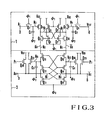
- a preferred embodiment.of the buffer circuit of this invention illustrated in Fig. 3 is constituted by a pre-circuit 1 which produces two opposite pre-signals A' o and A' o in response to an address designation input signal A I impressed upon an input terminal 3 and a reference voltage signal V REF impressed upon a reference voltage terminal 4, and a main circuit 2 supplied with the pre-output signals A' o and A' o for performing an address judgement to produce two output signals A o and A o of opposite phases and having predetermined levels.
- the pre-circuit 1 has the same construction as that 11 shown in Fig. 1. More particularly, the pre-circuit 1 is constituted by FETs Q 1 and Q 2 which form a flip-flop circuit cross-connected at nodes N 1 and N 21 with their source electrode common junction driven by a clock signal ⁇ 1 , D-FETs Q 3 and Q 4 respectively connected between the FETs Q l and Q 2 and a V DD source terminal with their gate electrodes commonly interconnected to be driven by the clock signal ⁇ 1 , D-FETs Q 5 and Q6 respectively connected between the nodes N 1 and N 2 and the V DD source terminal, FETs Q 7 and Q 8 respectively having drain electrodes for forming nodes N 3 and N 4 together with the gate electrodes of the D-FETs Q 5 and Q 6 , the gate electrodes of FETs Q 7 and Q 8 being driven by the clock signal ⁇ 1 and the source electrodes of the FETs Q 7 and Q 8 being connected to the input signal terminal 3 and the reference voltage signal terminal 4, respectively, boots
- the main circuit 2 is constituted by FETs Q11 and Q 12 cross-connected at nodes N 7 and N 8 to form a flip-flop circuit, the nodes N 7 and N 8 forming output terminals 5 and 6 of output signals A o and A respectively; FETs Q 13 and Q 14 with their source electrodes connected to nodes N 7 and N 8 and gate electrodes connected to nodes N 8 and N 7 respectively; FETs Q15 and Q 16 with their source electrodes connected to the drain electrodes of FETs Q13 and Q 14 respectively, drain electrodes connected to source electrodes of FETs Q 9 and Q 10 for forming the nodes N 5 and N 6 acting as output and input terminals of the pre-output signals A' and A' o , and the gate electrodes connected to the gate electrodes of FETs Q 14 and Q 13 respectively; FETs Q 17 and Q 18 with their source electrodes connected to the nodes N 7 and N 8 respectively, drain electrodes connected to the V DD source terminal, and gate electrodes connected to drain electrodes of F ET s Q
- the level of the clock signal P 1 is raised to the level of V DD , if necessary, higher than V DD to precharge the output nodes N 7 and N 8 to a sufficiently high level and the levels of the clock signals ⁇ 1 and ⁇ 2 are raised to a level slightly lower than that of the V DD .
- the input signal A I at the high level and the reference voltage signal V REF are applied to respective input terminals 3 and 4. Accordingly, both FETs Q 7 and Q 8 are turned ON to apply the input signal A I to the node N 3 and the reference voltage signal V REF to the node N 4 .
- the nodes N 1 and N 2 are precharged to the level of source V DD by the D-FETs Q 3 and Q 4 , and the flip-flop circuit constituted by FET s Q 1 and Q 2 is in an inoperative state.
- FETs Q 19 and Q 20 are turned ON to precharge the nodes N 7 and N 8 to the level of the source voltage VDD, with the result that FETs Q 13 and Q 14 are turned ON to precharge the nodes N 9 and N 10 to the level of the source voltage V DD .
- FETs Q 15 and Q 16 acting as a transfer gate are turned OFF since nodes N 5 and N 6 are charged to a high potential through FETs Q 9 and Q 10 , whereby the pre-circuit is disconnected from the main circuit.
- the level of the clock signal P 1 is lowered (to source potential V SS or ground potential), the clock signal ⁇ 2 is raised to a level slightly lower than that of the source voltage V DD and the clock signal ⁇ 1 is lowered to a low level. Accordingly, the nodes N 3 and N 4 are raised to high potentials by way of the bootstrap capacitors C 1 and C 2 to make different the capability of D-FETs Q 5 and Q 6 , which changes the potentials of the nodes N 1 and N 2 .
- the difference is judged by the flip-flop circuit constituted by FETs Q 1 and Q 2 and the result of judgement appears at the output nodes N 5 and N 6 of the pre-circuit via FETs Q 9 and Q 10 as the pre-output signals A' o and A' o .
- the potentials of nodes N 9 and N 10 are raised to levels higher than the level of the source voltage V DD by the clock signal ⁇ 2 through the medium of the bootstrap capacitors C 3 and C 4 .
- the potential level difference at nodes N 7 and N 8 is amplified and judged by the flip-flop circuit constituted by FETs Q 11 and Q 12 by lowering the level of the clock signal ⁇ 3 from high to low level to produce output signals A and A (in this case, A o is the low level signal) at the output terminals 5 and 6, respectively, and these output signals are positively fedback to the nodes N 9 and N 10 respectively throgh FETs Q13 and Q 14 .
- the FET Q16 automatically turns OFF since the potential of node N 10 is lowered as a result of turning ON of FET Q 14 due to the high potential of node N 7 , whereby the pre-circuit and the main circuit are disconnected again.
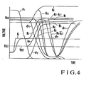
- Fig. 5 shows only the clock signals among various waveforms shown in Fig. 4 and the clock signals are depicted to correspond to those shown in Fig. 2.
- the circuit of this embodiment requires 4 clock signals P 1 , ⁇ 1 , ⁇ 2 and ⁇ 3 as shown in Fig. 5 just in the same manner as in the prior art.
- signal P 1 is used to precharge the output nodes N 7 and N 8 to a suitable potential, and may simply be of the same level as that of the source voltage VDD or more, if necessary. Accordingly, different from the clock signal P 11 necessary for directly driving the transfer gate as in the prior art, the clock signal P 1 is not required to have a high level like V DD and a strictly defined time spacing (see Fig. 2).
- the clock signal ⁇ 1 is a one shot opposit phase signal like the prior art for the purpose of decreasing the power consumption caused by the turning ON of the D-FETs 0 3 and Q 4 in the pre-circuit after the address judgement.
- the clock signal ⁇ 2 is used to drive the bootstrap capacitors C 1 , C 2 , C 3 and C 4 for raising the potentials of nodes N 3 , N 4 , N 9 and N 10 .
- the clock signal ⁇ 3 is used to activate the flip-flop circuit comprising FETs Q 11 and Q 12 for judging the address level and its level is changed from a level slightly lower than that of V DD to a much lower level, without requiring any special change. For this reason, in the circuit shown in Fig.
- the one necessary for the activation during judgement is not required to have strict voltage and time spacing so that it is not necessary to enlarge the time spacing, to use complicated circuit as well as large capacity transistors.
- the clock signal generating circuit can be readily designed, thus ensuring miniaturization and high speed operation of the memory circuit.
- the buffer circuit has been described by way of an address buffer circuit for a semiconductor memory device, the invention may also be applied to any circuits of a similar type.
- the buffer circuit of this invention is constituted by a pre-circuit producing two pre-output signals having opposite phases in response to an input signal; and a main circuit comprising a transfer gate circuit enabled by the pre-output signal and disabled by the output of the buffer circuit, a latch circuit for latching the pre-output signals, and a flip-flop circuit supplied with the pre-output signals latched by the latch circuit.
Landscapes
- Engineering & Computer Science (AREA)
- Microelectronics & Electronic Packaging (AREA)
- Computer Hardware Design (AREA)
- Logic Circuits (AREA)
- Static Random-Access Memory (AREA)
Abstract
Description
- This invention relates to a buffer circuit.
- A buffer circuit which produces two output signals having opposite phases (hereinafter termed opposite output signals) in response to a single input signal is constructed to compare the input signal.with a predetermined reference voltage signal for obtaining two opposite output signals and is important as a buffer element between an input circuit and an internal circuit in various electronic circuits. As the capacity of memory devices increases and as their operating speed increases, so an address buffer circuit for use with semiconductor memory devices becomes important. For this reason, in the following description, an address buffer circuit utilized in a semiconductor memory device is taken as a typical example.
- An address buffer circuit is used in a semiconductor memory device for sending an address selection designation signal to a decoding circuit in accordance with an address input signal, and it is strongly required in such an address buffer circuit that it can accurately judge a designated address and operate at a high sensitivity and high speed, that its power consumption is small, and that the address buffer circuit inclusive of a signal generating circuit can be designed readily and reduced in size for miniaturization of the chip.
- Various circuits have been proposed which meet these requirements. Fig. 1 shows one example of the most advanced prior art circuits.
- The circuit shown in Fig. 1 comprises a pre-circuit 11 essentially constituted by a flip-flop circuit which is made up of enhancement type field effect transistors (E-FET) Q31 and Q32 and which compares a single input signal AI with a predetermined reference voltage signal VREF to produce two opposite pre-output signals A' and
A' o , and amain circuit 12 essentially constituted by another flip-flop circuit made up of E-FETs Q41 and Q42 acting as a transfer gate which transfers the pre-output signals A'o andA' o A o when supplied with the pre-output signals A'o andA' o . One of the characteristic features of this circuit lies in that depletion type field effect transistors (D-FET) Q33, Q34, Q35 and Q36 are used in the pre-circuit. The operation of this circuit will be outlined as follows. - The operation of the pre-circuit will first be described. According to a clock signal φ11, the input signal A giving an address input and the reference voltage signal VREF are applied to nodes N13 and N14 via E-FETs (in the following merely designated as FET except D-FET) Q37 and Q38. While latching the applied signals by the clock signal φ11, a clock signal φ12 rises to raise the potential of these nodes N13 and N14 by the action of bootstrap capacitances C11 and C12. As a consequence, since the capability of D-FETs Q35 and Q36 are caused to vary by the applied input signal AI and reference voltage signal VREF. Such a change is judged by the flip-flop circuit constituted by FETs Q31 and Q32 by making a clock signal φ11 low level and the result of judgement appears at nodes N11 and N12 and is then sent out to the
main circuit 12 as the pre-output signals A'o andA' o A' o are applied to nodes N15 and N16 in themain circuit 12 in accordance with a clock signal P11 and then judged by the flip-flop circuit comprising FETs Q47 and Q48. Judged signals are outputted as output signals Ao and A fromoutput terminals A' o is maintained directly by a high level one of the output signals A andA' o - As described above, although this prior art circuit is advantageous in that its
main circuit 12 is simple and compact in construction, it still involves the following problems. For example, since the output information of the pre-circuit 11 which is transmitted to the nodes N15 and N16 is directly controlled by the output signals A andA o A o - Another prior art circuits also, require a clock signal that rises to the VDD source voltage level at the time of judgement. In addition, there is the problem of time spacing described above. Accordingly, the requirement for clock signal generating circuit is severe, which makes it complex and difficult to design the circuit and prevents miniaturization of the circuit and high speed operation thereof.
- Accordingly, it is an object of this invention to provide an improved buffer circuit in which the requirements for the voltage and time spacing of clock signals necessary for judgement (operation) are not so severe as in the prior art buffer circuit so that the clock signal generating circuit can be designed readily to have a compact size and can operate at a high speed.
- According to this invention, there is provided a buffer circuit which produces two output signals of the opposite phases in response to an input signal, characterized in that there are provided a pre-circuit producing two pre-output signals in accordance with the input signal and a reference voltage signal; and a main circuit including a transfer gate circuit enabled by the pre-output signals and disabled by the output signals of the buffer circuit, a latch circuit latching the pre-output signals, and a flip-flop circuit connected to receive the pre-output signals latched by the latch circuit for producing the output signals of the buffer circuit.
- In the accompanying drawings:
- Fig. 1 shows a connection diagram of a prior art buffer circuit;
- Fig. 2 shows waveforms of clock signal voltages utilized in the circuit shown in Fig. 1;
- Fig. 3 is a connection diagram showing one embodiment of the buffer circuit according to this invention;
- Fig. 4 shows waveforms of node potentials and clock signal voltages of the circuit shown in Fig. 3; and
- Fig. 5 shows waveforms of the clock signal voltages utilized in the circuit shown in Fig. 3.
- A preferred embodiment.of the buffer circuit of this invention illustrated in Fig. 3 is constituted by a pre-circuit 1 which produces two opposite pre-signals A'o and
A' o input terminal 3 and a reference voltage signal VREF impressed upon a reference voltage terminal 4, and amain circuit 2 supplied with the pre-output signals A'o andA' o A o - The pre-circuit 1 has the same construction as that 11 shown in Fig. 1. More particularly, the pre-circuit 1 is constituted by FETs Q1 and Q2 which form a flip-flop circuit cross-connected at nodes N1 and N21 with their source electrode common junction driven by a clock signal φ1, D-FETs Q3 and Q4 respectively connected between the FETs Ql and Q2 and a VDD source terminal with their gate electrodes commonly interconnected to be driven by the clock signal φ1, D-FETs Q5 and Q6 respectively connected between the nodes N1 and N2 and the VDD source terminal, FETs Q7 and Q8 respectively having drain electrodes for forming nodes N3 and N4 together with the gate electrodes of the D-FETs Q5 and Q6, the gate electrodes of FETs Q7 and Q8 being driven by the clock signal φ1 and the source electrodes of the FETs Q7 and Q8 being connected to the
input signal terminal 3 and the reference voltage signal terminal 4, respectively, bootstrap capacitors C1 and C2 respectively connected to the nodes N3 and N4 to be driven by a clock signal φ2, and FETs Q9 and Q10 with their drain electrodes connected to the nodes N1 and N2, the gate electrodes commonly connected to the gate electrodes of FETs Q1 and Q2 and source electrode acting as output nodes N5 and N6 of the pre-output signals A'o andA' o . - The
main circuit 2 is constituted by FETs Q11 and Q12 cross-connected at nodes N7 and N8 to form a flip-flop circuit, the nodes N7 and N8 formingoutput terminals A respectively; FETs Q13 and Q14 with their source electrodes connected to nodes N7 and N8 and gate electrodes connected to nodes N8 and N7 respectively; FETs Q15 and Q16 with their source electrodes connected to the drain electrodes of FETs Q13 and Q14 respectively, drain electrodes connected to source electrodes of FETs Q9 and Q10 for forming the nodes N5 and N6 acting as output and input terminals of the pre-output signals A' andA' o , and the gate electrodes connected to the gate electrodes of FETs Q14 and Q13 respectively; FETs Q17 and Q18 with their source electrodes connected to the nodes N7 and N8 respectively, drain electrodes connected to the VDD source terminal, and gate electrodes connected to drain electrodes of FETs Q13 and Q14 to form nodes N9 and N10; bootstrap capacitors C3 and C4 respectively connected to the nodes N9 and N10 and driven by a clock signal φ2; and FETs Q19 and Q20 with their source electrodes connected to the nodes N7 and N8, drain electrodes connected to the VDD source terminal, and gate electrodes connected to be driven by a clock signal P1. The flip-flop circuit comprised of the FETs Q11 and Q12 is connected to receive a clock pulse φ3. - The operation of the embodiment shown in Fig. 3 will now be described with reference to the node potentials and clock signal voltages shown in Fig. 4. For the sake of description, it is assumed that the input signal AI is at a high level.
- Firstly, the level of the clock signal P1 is raised to the level of VDD, if necessary, higher than VDD to precharge the output nodes N7 and N8 to a sufficiently high level and the levels of the clock signals φ1 and φ2 are raised to a level slightly lower than that of the VDD. The input signal AI at the high level and the reference voltage signal VREF are applied to
respective input terminals 3 and 4. Accordingly, both FETs Q7 and Q8 are turned ON to apply the input signal AI to the node N3 and the reference voltage signal VREF to the node N4. Also the nodes N1 and N2 are precharged to the level of source VDD by the D-FETs Q3 and Q4, and the flip-flop circuit constituted by FETs Q1 and Q2 is in an inoperative state. On the other hand, in the main circuit, FETs Q19 and Q20 are turned ON to precharge the nodes N7 and N8 to the level of the source voltage VDD, with the result that FETs Q13 and Q14 are turned ON to precharge the nodes N9 and N10 to the level of the source voltage VDD. Thus, FETs Q15 and Q16 acting as a transfer gate are turned OFF since nodes N5 and N6 are charged to a high potential through FETs Q9 and Q10, whereby the pre-circuit is disconnected from the main circuit. - Then, the level of the clock signal P1 is lowered (to source potential VSS or ground potential), the clock signal φ2 is raised to a level slightly lower than that of the source voltage VDD and the clock signal φ1 is lowered to a low level. Accordingly, the nodes N3 and N4 are raised to high potentials by way of the bootstrap capacitors C1 and C2 to make different the capability of D-FETs Q5 and Q6, which changes the potentials of the nodes N1 and N2. The difference is judged by the flip-flop circuit constituted by FETs Q1 and Q2 and the result of judgement appears at the output nodes N5 and N6 of the pre-circuit via FETs Q9 and Q10 as the pre-output signals A'o and
A' o . On the other hand, in the main circuit, the potentials of nodes N9 and N10 are raised to levels higher than the level of the source voltage VDD by the clock signal φ2 through the medium of the bootstrap capacitors C3 and C4. - Under this state, when the pre-output signals A' and A from the pre-circuit appear at nodes N5 and N6, the FET Q16 on the lower level side (since at this time the input signal AI is at the high level, signal
A' o is at the low level) acting as a transfer gate is turned ON to lower the potential of the node N10 to a low level. As a consequence, the capability of FETs Q17 and Q18 is greatly varied whereby the potentials of nodes N7 and N8 vary correspondingly. In other words, the output signals A'o andA' o of the pre-circuit are latched by FETs Q17 and Q18. The potential level difference at nodes N7 and N8 is amplified and judged by the flip-flop circuit constituted by FETs Q11 and Q12 by lowering the level of the clock signal φ3 from high to low level to produce output signals A and A (in this case, Ao is the low level signal) at theoutput terminals main circuit 2 will not be influenced. Fig. 5 shows only the clock signals among various waveforms shown in Fig. 4 and the clock signals are depicted to correspond to those shown in Fig. 2. - As described above, the circuit of this embodiment requires 4 clock signals P1, φ1, φ2 and φ3 as shown in Fig. 5 just in the same manner as in the prior art. However, signal P1 is used to precharge the output nodes N7 and N8 to a suitable potential, and may simply be of the same level as that of the source voltage VDD or more, if necessary. Accordingly, different from the clock signal P11 necessary for directly driving the transfer gate as in the prior art, the clock signal P1 is not required to have a high level like VDD and a strictly defined time spacing (see Fig. 2). The clock signal φ1 is a one shot opposit phase signal like the prior art for the purpose of decreasing the power consumption caused by the turning ON of the D-FETs 03 and Q4 in the pre-circuit after the address judgement.
- The clock signal φ2 is used to drive the bootstrap capacitors C1, C2, C3 and C4 for raising the potentials of nodes N3, N4, N9 and N10. According to this invention, although the number of the nodes whose potentials are to be increased by 2 as compared to the prior art circuit, the high level is lower than that of the source voltage VDD, thus causing no problem. The clock signal φ3 is used to activate the flip-flop circuit comprising FETs Q11 and Q12 for judging the address level and its level is changed from a level slightly lower than that of VDD to a much lower level, without requiring any special change. For this reason, in the circuit shown in Fig. 3, it is not necessary to use such the strictly defined strong signal φ13 (shown in Fig. 2) adapted to directly drive a load, which signal is required to have strict time spacings with respect to other signals as in the prior art circuit, and further required to have a higher level than VDD sufficient to self-boot the nodes N17 and N18 (see Fig. 1) to above V DD.
- Thus, according to the circuit shown in Fig. 3, among various clock signals, the one necessary for the activation during judgement is not required to have strict voltage and time spacing so that it is not necessary to enlarge the time spacing, to use complicated circuit as well as large capacity transistors. Thus, the clock signal generating circuit can be readily designed, thus ensuring miniaturization and high speed operation of the memory circuit.
- Although, in the foregoing embodiment, the buffer circuit has been described by way of an address buffer circuit for a semiconductor memory device, the invention may also be applied to any circuits of a similar type.
- As described above, the buffer circuit of this invention is constituted by a pre-circuit producing two pre-output signals having opposite phases in response to an input signal; and a main circuit comprising a transfer gate circuit enabled by the pre-output signal and disabled by the output of the buffer circuit, a latch circuit for latching the pre-output signals, and a flip-flop circuit supplied with the pre-output signals latched by the latch circuit. As a consequence, different from the prior art circuit, it is not necessary to use any strong clock signal required to have high levels equal to the level of the source voltage VDD and strict time spacing during the activation (judging operation) of the circuit, thereby simplifying the design of the clock signal generating circuit, miniaturizing the entire circuit and increasing the operating speed.
Claims (3)
Applications Claiming Priority (2)
| Application Number | Priority Date | Filing Date | Title |
|---|---|---|---|
| JP16121/82 | 1982-02-03 | ||
| JP57016121A JPS58133024A (en) | 1982-02-03 | 1982-02-03 | Buffer circuit |
Publications (3)
| Publication Number | Publication Date |
|---|---|
| EP0085436A2 true EP0085436A2 (en) | 1983-08-10 |
| EP0085436A3 EP0085436A3 (en) | 1986-02-05 |
| EP0085436B1 EP0085436B1 (en) | 1989-04-26 |
Family
ID=11907676
Family Applications (1)
| Application Number | Title | Priority Date | Filing Date |
|---|---|---|---|
| EP83101022A Expired EP0085436B1 (en) | 1982-02-03 | 1983-02-03 | Buffer circuits |
Country Status (4)
| Country | Link |
|---|---|
| US (1) | US4542306A (en) |
| EP (1) | EP0085436B1 (en) |
| JP (1) | JPS58133024A (en) |
| DE (1) | DE3379759D1 (en) |
Cited By (1)
| Publication number | Priority date | Publication date | Assignee | Title |
|---|---|---|---|---|
| US4845676A (en) * | 1986-02-21 | 1989-07-04 | International Business Machines Corporation | Non-clocked static memory cell |
Families Citing this family (14)
| Publication number | Priority date | Publication date | Assignee | Title |
|---|---|---|---|---|
| US4604534A (en) * | 1984-12-03 | 1986-08-05 | International Business Machines Corporation | Highly sensitive high performance sense amplifiers |
| US4952826A (en) * | 1985-07-05 | 1990-08-28 | Nec Corporation | Signal input circuit utilizing flip-flop circuit |
| JPS628614A (en) * | 1985-07-05 | 1987-01-16 | Nec Corp | Input inverter circuit |
| JPS629590A (en) * | 1985-07-08 | 1987-01-17 | Nec Corp | Amplifier circuit |
| JPS6218112A (en) * | 1985-07-16 | 1987-01-27 | Toshiba Corp | Flip-flop circuit |
| JPS62205597A (en) * | 1986-03-05 | 1987-09-10 | Toshiba Corp | Semiconductor sensing amplifying circuit |
| EP0254980B1 (en) * | 1986-07-24 | 1991-09-25 | Siemens Aktiengesellschaft | Integrated sense amplifier circuit |
| JPH0284811A (en) * | 1988-01-30 | 1990-03-26 | Nec Corp | Input inverter circuit |
| US4859880A (en) * | 1988-06-16 | 1989-08-22 | International Business Machines Corporation | High speed CMOS differential driver |
| US5546036A (en) * | 1992-08-27 | 1996-08-13 | Siemens Aktiengesellschaft | Circuit array for amplifying and holding data with different supply |
| US5491428A (en) * | 1993-12-20 | 1996-02-13 | Hitachi Microsystems, Inc. | Bus-isolating pre-charge buffer |
| TW445714B (en) * | 2000-05-05 | 2001-07-11 | Ind Tech Res Inst | Capacitor-coupled differential logic circuit |
| KR200204564Y1 (en) * | 2000-07-01 | 2000-12-01 | 임지중 | A device for measuring swing velocity of the golf club head using the resonance circuit |
| US9235047B2 (en) * | 2011-06-01 | 2016-01-12 | Pixtronix, Inc. | MEMS display pixel control circuits and methods |
Citations (1)
| Publication number | Priority date | Publication date | Assignee | Title |
|---|---|---|---|---|
| EP0036743A1 (en) * | 1980-03-18 | 1981-09-30 | Fujitsu Limited | TTL- to MOS-level address buffer circuit |
Family Cites Families (5)
| Publication number | Priority date | Publication date | Assignee | Title |
|---|---|---|---|---|
| DE2855118C2 (en) * | 1978-12-20 | 1981-03-26 | IBM Deutschland GmbH, 70569 Stuttgart | Dynamic FET memory |
| JPS56101694A (en) * | 1980-01-18 | 1981-08-14 | Nec Corp | Semiconductor circuit |
| JPS6037996B2 (en) * | 1980-02-20 | 1985-08-29 | 沖電気工業株式会社 | buffer circuit |
| US4354257A (en) * | 1980-05-23 | 1982-10-12 | Fairchild Camera And Instrument Corporation | Sense amplifier for CCD memory |
| US4441039A (en) * | 1981-11-20 | 1984-04-03 | International Business Machines Corporation | Input buffer circuit for semiconductor memory |
-
1982
- 1982-02-03 JP JP57016121A patent/JPS58133024A/en active Granted
-
1983
- 1983-02-02 US US06/463,338 patent/US4542306A/en not_active Expired - Lifetime
- 1983-02-03 DE DE8383101022T patent/DE3379759D1/en not_active Expired
- 1983-02-03 EP EP83101022A patent/EP0085436B1/en not_active Expired
Patent Citations (1)
| Publication number | Priority date | Publication date | Assignee | Title |
|---|---|---|---|---|
| EP0036743A1 (en) * | 1980-03-18 | 1981-09-30 | Fujitsu Limited | TTL- to MOS-level address buffer circuit |
Non-Patent Citations (1)
| Title |
|---|
| IEEE INTERNATIONAL SOLID-STATE CIRCUITS CONFERENCE ISSCC 1979, DIGEST OF TECHNICAL PAPERS, 15th February 1979, IEEE, New York, US; J.M. LEE et al.: "Dynamic memories: THPM 12.2: A 80ns 5V-only dynamic RAM" * |
Cited By (1)
| Publication number | Priority date | Publication date | Assignee | Title |
|---|---|---|---|---|
| US4845676A (en) * | 1986-02-21 | 1989-07-04 | International Business Machines Corporation | Non-clocked static memory cell |
Also Published As
| Publication number | Publication date |
|---|---|
| DE3379759D1 (en) | 1989-06-01 |
| JPH0159677B2 (en) | 1989-12-19 |
| US4542306A (en) | 1985-09-17 |
| EP0085436A3 (en) | 1986-02-05 |
| JPS58133024A (en) | 1983-08-08 |
| EP0085436B1 (en) | 1989-04-26 |
Similar Documents
| Publication | Publication Date | Title |
|---|---|---|
| US4389705A (en) | Semiconductor memory circuit with depletion data transfer transistor | |
| EP0092809B1 (en) | Logic circuit having voltage booster | |
| EP0045133B1 (en) | Bootstrap driver circuits for an mos memory | |
| US5349247A (en) | Enhancement circuit and method for ensuring diactuation of a switching device | |
| US4123799A (en) | High speed IFGET sense amplifier/latch | |
| US4176289A (en) | Driving circuit for integrated circuit semiconductor memory | |
| JP2723278B2 (en) | Decoder / driver circuit for high capacitance line programming | |
| EP0098060B1 (en) | Clock pulse generating circuit | |
| EP0085436A2 (en) | Buffer circuits | |
| US4284905A (en) | IGFET Bootstrap circuit | |
| US5546338A (en) | Fast voltage equilibration of differential data lines | |
| JP2862744B2 (en) | Data output buffer of semiconductor memory device | |
| JPH0355913B2 (en) | ||
| US4649289A (en) | Circuit for maintaining the potential of a node of a MOS dynamic circuit | |
| US4570244A (en) | Bootstrap driver for a static RAM | |
| US5517142A (en) | Output buffer with a reduced transient bouncing phenomenon | |
| US4431927A (en) | MOS Capacitive bootstrapping trigger circuit for a clock generator | |
| US4970693A (en) | Semiconductor memory device with internal control signal based upon output timing | |
| EP0259861A1 (en) | Buffer circuit operable with reduced power consumption | |
| US4451907A (en) | Pull-up circuit for a memory | |
| EP0168246A2 (en) | Improved active pull-up circuit | |
| US4352996A (en) | IGFET Clock generator circuit employing MOS boatstrap capacitive drive | |
| US4091360A (en) | Dynamic precharge circuitry | |
| JP2000021179A (en) | Boosting circuit and semiconductor device using the same | |
| JP2527050B2 (en) | Sense amplifier circuit for semiconductor memory |
Legal Events
| Date | Code | Title | Description |
|---|---|---|---|
| PUAI | Public reference made under article 153(3) epc to a published international application that has entered the european phase |
Free format text: ORIGINAL CODE: 0009012 |
|
| AK | Designated contracting states |
Designated state(s): DE FR GB |
|
| RAP1 | Party data changed (applicant data changed or rights of an application transferred) |
Owner name: NEC CORPORATION |
|
| 17P | Request for examination filed |
Effective date: 19840418 |
|
| PUAL | Search report despatched |
Free format text: ORIGINAL CODE: 0009013 |
|
| AK | Designated contracting states |
Designated state(s): DE FR GB |
|
| 17Q | First examination report despatched |
Effective date: 19870611 |
|
| GRAA | (expected) grant |
Free format text: ORIGINAL CODE: 0009210 |
|
| AK | Designated contracting states |
Kind code of ref document: B1 Designated state(s): DE FR GB |
|
| REF | Corresponds to: |
Ref document number: 3379759 Country of ref document: DE Date of ref document: 19890601 |
|
| ET | Fr: translation filed | ||
| PLBE | No opposition filed within time limit |
Free format text: ORIGINAL CODE: 0009261 |
|
| STAA | Information on the status of an ep patent application or granted ep patent |
Free format text: STATUS: NO OPPOSITION FILED WITHIN TIME LIMIT |
|
| 26N | No opposition filed | ||
| PGFP | Annual fee paid to national office [announced via postgrant information from national office to epo] |
Ref country code: GB Payment date: 19920124 Year of fee payment: 10 |
|
| PGFP | Annual fee paid to national office [announced via postgrant information from national office to epo] |
Ref country code: FR Payment date: 19920221 Year of fee payment: 10 |
|
| PGFP | Annual fee paid to national office [announced via postgrant information from national office to epo] |
Ref country code: DE Payment date: 19920416 Year of fee payment: 10 |
|
| PG25 | Lapsed in a contracting state [announced via postgrant information from national office to epo] |
Ref country code: GB Effective date: 19930203 |
|
| GBPC | Gb: european patent ceased through non-payment of renewal fee |
Effective date: 19930203 |
|
| PG25 | Lapsed in a contracting state [announced via postgrant information from national office to epo] |
Ref country code: FR Effective date: 19931029 |
|
| PG25 | Lapsed in a contracting state [announced via postgrant information from national office to epo] |
Ref country code: DE Effective date: 19931103 |
|
| REG | Reference to a national code |
Ref country code: FR Ref legal event code: ST |