EP0080841B1 - Dual coupler fiber optic recirculating memory - Google Patents
Dual coupler fiber optic recirculating memory Download PDFInfo
- Publication number
- EP0080841B1 EP0080841B1 EP82306164A EP82306164A EP0080841B1 EP 0080841 B1 EP0080841 B1 EP 0080841B1 EP 82306164 A EP82306164 A EP 82306164A EP 82306164 A EP82306164 A EP 82306164A EP 0080841 B1 EP0080841 B1 EP 0080841B1
- Authority
- EP
- European Patent Office
- Prior art keywords
- fiber
- optical
- strand
- input
- output
- Prior art date
- Legal status (The legal status is an assumption and is not a legal conclusion. Google has not performed a legal analysis and makes no representation as to the accuracy of the status listed.)
- Expired - Lifetime
Links
Images


Classifications
-
- G—PHYSICS
- G02—OPTICS
- G02B—OPTICAL ELEMENTS, SYSTEMS OR APPARATUS
- G02B6/00—Light guides; Structural details of arrangements comprising light guides and other optical elements, e.g. couplings
- G02B6/24—Coupling light guides
- G02B6/26—Optical coupling means
- G02B6/28—Optical coupling means having data bus means, i.e. plural waveguides interconnected and providing an inherently bidirectional system by mixing and splitting signals
- G02B6/293—Optical coupling means having data bus means, i.e. plural waveguides interconnected and providing an inherently bidirectional system by mixing and splitting signals with wavelength selective means
- G02B6/29331—Optical coupling means having data bus means, i.e. plural waveguides interconnected and providing an inherently bidirectional system by mixing and splitting signals with wavelength selective means operating by evanescent wave coupling
- G02B6/29335—Evanescent coupling to a resonator cavity, i.e. between a waveguide mode and a resonant mode of the cavity
- G02B6/29338—Loop resonators
-
- G—PHYSICS
- G02—OPTICS
- G02B—OPTICAL ELEMENTS, SYSTEMS OR APPARATUS
- G02B6/00—Light guides; Structural details of arrangements comprising light guides and other optical elements, e.g. couplings
- G02B6/24—Coupling light guides
- G02B6/26—Optical coupling means
- G02B6/28—Optical coupling means having data bus means, i.e. plural waveguides interconnected and providing an inherently bidirectional system by mixing and splitting signals
- G02B6/2804—Optical coupling means having data bus means, i.e. plural waveguides interconnected and providing an inherently bidirectional system by mixing and splitting signals forming multipart couplers without wavelength selective elements, e.g. "T" couplers, star couplers
- G02B6/2821—Optical coupling means having data bus means, i.e. plural waveguides interconnected and providing an inherently bidirectional system by mixing and splitting signals forming multipart couplers without wavelength selective elements, e.g. "T" couplers, star couplers using lateral coupling between contiguous fibres to split or combine optical signals
-
- G—PHYSICS
- G02—OPTICS
- G02B—OPTICAL ELEMENTS, SYSTEMS OR APPARATUS
- G02B6/00—Light guides; Structural details of arrangements comprising light guides and other optical elements, e.g. couplings
- G02B6/24—Coupling light guides
- G02B6/26—Optical coupling means
- G02B6/28—Optical coupling means having data bus means, i.e. plural waveguides interconnected and providing an inherently bidirectional system by mixing and splitting signals
- G02B6/2804—Optical coupling means having data bus means, i.e. plural waveguides interconnected and providing an inherently bidirectional system by mixing and splitting signals forming multipart couplers without wavelength selective elements, e.g. "T" couplers, star couplers
- G02B6/2861—Optical coupling means having data bus means, i.e. plural waveguides interconnected and providing an inherently bidirectional system by mixing and splitting signals forming multipart couplers without wavelength selective elements, e.g. "T" couplers, star couplers using fibre optic delay lines and optical elements associated with them, e.g. for use in signal processing, e.g. filtering
-
- G—PHYSICS
- G02—OPTICS
- G02B—OPTICAL ELEMENTS, SYSTEMS OR APPARATUS
- G02B6/00—Light guides; Structural details of arrangements comprising light guides and other optical elements, e.g. couplings
- G02B6/24—Coupling light guides
- G02B6/26—Optical coupling means
- G02B6/28—Optical coupling means having data bus means, i.e. plural waveguides interconnected and providing an inherently bidirectional system by mixing and splitting signals
- G02B6/293—Optical coupling means having data bus means, i.e. plural waveguides interconnected and providing an inherently bidirectional system by mixing and splitting signals with wavelength selective means
- G02B6/29331—Optical coupling means having data bus means, i.e. plural waveguides interconnected and providing an inherently bidirectional system by mixing and splitting signals with wavelength selective means operating by evanescent wave coupling
- G02B6/29332—Wavelength selective couplers, i.e. based on evanescent coupling between light guides, e.g. fused fibre couplers with transverse coupling between fibres having different propagation constant wavelength dependency
Definitions
- a recirculating memory In a recirculating memory, data is injected into a closed loop at a high rate, and recirculates around the loop in a continuous unidirectional motion.
- the entire group of data stored in the loop may be repeatedly read from the loop at a period equal to the time taken for the data to complete one cycle around the loop.
- a group of data may be stored in the recirculating memory, and the data may be read from the memory at a slower rate since the data will continue to circulate in the loop for some extended period of time, thus allowing different portions of the data to be sampled after each circulation.
- Such systems are quite useful in applications where data is generated at a rate faster than it can be accepted by a data processor.
- a recirculating memory between the data source and the data processor, the data can be supplied to the data processor at the rate necessary for the data processor to analyze the data without losing any of it.
- Another use of recirculating memory devices is for the temporary storage and retrieval of broadband microwave signals in electronic counter-measures (ECM) used to jam radar signals or to project false radar images.
- ECM electronic counter-measures
- Such devices are basically delay lines in which a time delay is produced because of the time a signal takes to travel through the delay lines from the input end to the output end.
- a portion of that signal will be reflected and will propagate from the output end back to the input end, where it is reflected to the output end again, resulting in a second output signal identical to the first output signal, although smaller in amplitude.
- the data pulse will continue to be reflected and outputted from the delay lines for some period of time, resulting in a number of identical pulses, equidistantly spaced, with decreasing amplitude.
- the coaxial cable delay line is the most common type of delay line, and microwave signals may be stored in coaxial cables for some period of time.
- Coaxial cable may be used with directional couplers, which couple a secondary system to a wave traveling in a particular direction in the primary transmission system.
- coaxial delay lines have several disadvantages.
- the first disadvantage is the limited bandwidth of coaxial cable, making coaxial cable useless at high frequencies and with short pulses.
- coaxial cable is subject to severe losses, and high frequencies will thus not be transmitted accurately.
- the pulse being transmitted is of extremely short duration, e.g., one nanosecond, it will be degraded and spread out rather than remaining sharp. This limits the number of pulses which can be transmitted close together, and, consequently, the information-carrying capability of the coaxial cable.
- a second disadvantage of coaxial cable is that it is susceptible to electromagnetic interference, particularly when the frequencies being transmitted are relatively high.
- a coaxial cable delay line with a sufficiently long delay time a considerable length of coaxial cable is necessary. Such delay lines are quite bulky, and also fairly expensive.
- a second technique utilized to create delay lines and recirculating memories is through the use of acoustic delay lines.
- acoustic delay lines There are two types of acoustic delay lines: bulk-wave devices, and surface-wave devices.
- Bulk-wave devices use the principle of compression and rarification of the bulk material, and have input and output transducers at the ends of the bulk material.
- Bulk-wave devices unfortunately require large bias voltages and thus present a heat dissipation problem, so that only pulsed operation of bulk-wave devices is feasible.
- Surface-wave devices operate with acoustic surface waves, and utilize charge carriers in a thin film of silicon placed adjacent to an insulating piezoelectric crystal.
- Surface acoustic wave memories operating at UHF frequencies have been developed.
- the main disadvantage of such acoustic wave memories is that their upper operational frequency limit is approximately 1 GHZ, while it is desirable to have a recirculating memory operable at higher frequencies.
- a second problem with the Suzaki apparatus is that it does not utilize evanescent field coupling in the coupling device utilized.
- the coupling device utilized requires that the glass fibers be cut and polished until the cores of the fibers are exposed to create an optical couple between the fibers. This presents the possibility that the core of the fiber may be damaged in the process, further lowering the efficiency of the Suzaki device.
- the coupling loss which is the difference between the amount of light going into the coupler and the amount of light coming out of the coupler, may be significant.
- the Suzaki device cannot fulfill the two following conflicting requirements: (1) provide a great number of recirculations through the loop; and (2) provide a small measurement window between the initial output pulses.
- the Suzaki device utilizes multi-mode fibers rather than single mode fibers.
- Multi-mode fibers have a much larger core diameter than do single mode fibers. Since multi-mode fibers have a larger core, the angle of refraction is greater, and thus multi-mode fibers are quite susceptible to modal dispersion, which will limit the bandwidth to 500 MHz to 1 GHz. Even when using a graded index multi-mode fiber, where dispersion is minimized by grading of the index of refraction, maximum bandwidth of signals to be transmitted is only slightly above 1 GHz. The exact bandwidth, of course, will depend on the frequency of the light, since light of a given wavelength may have minimal dispersion due to properties of the optical fiber.
- Single-mode fiber does not have modal dispersion problems, since the diameter of the single-mode fiber core is relatively small. While any optical fiber will have some material dispersion, the effects of material dispersion are several orders of magnitude less than those of modal dispersion.
- the Suzaki device possesses the disadvantages of having a limited bandwidth and of having relatively high losses, which impedes the transmission of a pulse train of any length. For these reasons, the Suzaki device is not useful as a recirculating memory device with a high frequency data input.
- the present invention as defined in Claim 1 is a fiber optic recirculating memory device comprising a first strand of optical fiber, having an input end for receiving optical input signals and an output end for providing optical output signals, a second strand of optical fiber forming a loop, the second strand having a first end portion and a second end portion at each end of the strand.
- the memory device of the present invention further comprises a first optical fiber coupler for coupling the first strand and the first end portion of the second strand.
- the fiber optic recirculating memory device of the present invention is characterized by a second optical fiber coupler for coupling the first strand and the second end portion of the second strand.
- the second optical coupler coupling a portion of optical signals propagating in the first strand into the second strand, and the first optical coupler coupling a portion of optical signals propagating in the second strand into the first strand.
- the second strand has a length sufficiently large so as to create a predetermined delay time between the coupling of an optical signal from the second strand into the first strand.
- the length is selected so that the delay time is greater than the signal duration of the signal received at the input end.
- the first strand and the second strand are single mode optical fibers.
- the first and second optical couplers use evanescent field coupling to couple light between the first and second strands and each have coupling efficiencies greater than 50%.
- the sequence of output signals from the output end is a sequence of pulses with the sequence including a number n of pulses having at least a predetermined signal level with n being calculated by the formula where p T /P o is the ratio of the minimum detectable output power level to the power level of the light input, 1 1 and 1 2 are the coupling efficiencies of the first and second couplers, respectively, and K is the percentage of power transmitted by the second strand.
- the present invention also discloses a method of producing a number of output pulses utilizing the fiber optic recirculating memory device of the present invention as defined in Claim 1.
- the present application discloses a method of producing a series of output signals utilizing a fiber optic recirculating memory device having a first strand of optical fiber having an input fiber portion for receiving optical input signals and an output fiber portion for providing optical output signals, a second strand of optical fiber forming a fiber loop portion, the fiber loop portion being coupled to the input fiber portion via a first optical fiber coupler and to the output fiber portion via a second optical fiber coupler, the output signals being substantially identical in waveform to a signal input at the input fiber portion of the device, the method comprising the steps of:
- a method of manufacturing a fiber optic recirculating memory device of the kind defined in Claim 1 comprising the steps of forming a loop portion using an optical fiber which has a first end portion and a second end portion at each end of the fiber;
- the invention also discloses the use of a fiber optic recirculating memory according to Claim 1 as a transversal filter.
- FIG. 1 a fiber optic directional optic coupler which may be used to form a recirculating loop memory is shown.
- the following description of Figures 1 through 4 provides an understanding of the essential characteristics of the fiber optic coupler.
- the coupler 10 includes two strands, 12a and 12b, of a single mode fiber optic material mounted in longitudinal arcuate grooves 13a and 13b, respectively, formed in optically flat confronting surfaces 14a and 14b, respectively, of rectangular bases or substrates 16a and 16b, respectively.
- Each of the strands 12a and 12b comprises a commercially available fiber of quartz glass which is doped to have a central core 11 a, 11 b and an outer cladding 15a, 15b, respectively.
- the applicant has found that the present invention works effectively with single mode fibers, which typically have a core diameter in the order of 10 microns or less, and a cladding diameter on the order of 125 microns.
- the arcuate grooves 13a and 13b have a radius of curvature which is very large compared to the diameters of the strands 12.
- the fiber optic strands 12a and 12b when mounted in the grooves 13a and 13b, respectively, gradually converge toward the center and diverge toward the edges of the substrates 16a and 16b.
- the depth of the grooves 13 which mount strands 12 is less than the diameter of the strands 12, while at the edges of the blocks 16, the depth of the grooves 13 is preferably at least as great as the diameter of the strands 12.
- Fiber optic material is removed from each of the strands 12a and 12b to form respective oval shaped, planar surfaces 18a, 18b which are co-planar with the confronting surfaces 17a, 17b, respectively, of the substrates 16a and 16b, respectively.
- the coupler halves 10A and 10B are identical and are assembled by placing the confronting surfaces 14A and 14B of the substrates 16a and 16b together so that the surfaces 18a and 18b of the strands 12a and 12b are in facing relationship.
- An index matching substance (not shown), such as index matching oil, is provided between the confronting surfaces 14. This substance has a refractive index approximately equal to the refractive index of the cladding 15 and also functions to prevent the optically flat surfaces 14 from becoming permanently locked together.
- An interaction region 32 is formed at the junction of the strands 12. In this region 32 light is transferred between the strands 12a, 12b by evanescent field coupling.
- each strand 12a, 12b receives a significant portion of the evanescent field energy from the other strand 12a, 12b and optimum coupling is achieved without significant energy loss.
- the critical zone can be quite narrow.
- the required center-to- center spacing between the strands 12 at the center of the coupler is typically less than a few (for example, 2-3) core diameters.
- the strands 12a and 12b are symmetrical through the interaction region 32 in the plane of the facing surfaces 18 so that the facing surfaces 18a and 18b are coextensive if superimposed.
- the coupler 10 includes four ports labeled A, B, C and D in Figure 1. If it is assumed that input light of a suitable wavelength (for example, 1.15 microns) is applied to port A, this light passes through the coupler and is output at port B and/or port D, depending on the amount of power that is coupled between the strands 12.
- a suitable wavelength for example, 1.15 microns
- the term "normalized coupled power” is defined as the power ratio of the coupled power to the total output power. In the above example, the normalized coupled power would be equal to the ratio of the power at port D to the sum of the power output at ports B and D. This ratio is also referred to as the "coupling efficiency" and when so used is typically expressed as a percent. Thus, when the term "normalized coupled power” is used herein, it should be understood that the corresponding “coupling efficiency” is equal to the normalized coupled power times 100.
- the coupler 10 operates on evanescent field coupling principles in which guided modes of the strands 12 interact through their evanescent fields to cause light to be transferred between the strands 12. As previously indicated, this transfer of light occurs at the interaction region 32. The amount of light transferred is dependent upon the proximity and orientation of the cores as well as the effective length of the interaction region 32. If the length of the interaction region 32 and the separation of the strands 12 within this region 32 are properly selected, light within the coupler will make only one transfer between the strands 12 as it travels through the interaction region 32. If the coupler is properly constructed, it is possible under such conditions to couple 100% of the light input at port A to port D.
- a single continuous length of optical fiber 12 is used.
- the input end 142 of the fiber 12 enters the optical coupler 10 through port C, and exits the coupler 10 from port D.
- a length of the fiber 12 for example 200 meters, is formed into a loop 140.
- the fiber 12 then leaves the loop 140 and enters the coupler 10 through port A, and exits from port B.
- the end of the fiber 12 which exits the coupler 10 through port B is the output end 144 of the fiber 12.
- An input signal 160 of modulated light pulses shown in Figure 6, is supplied to the input end 142 of the optical fiber 12 at the time T 1 , from a laser light source 150 and a modulator 152. This light will enter the optical coupler 10 through port C. Assuming a typical coupling efficiency of 95%, 95% of the light will be coupled to the port B. Light exiting the coupler from port B leaves the optical fiber 12 through the fiber exit 144 at time T 2 which is an instant after T 1 , and this is the first output signal 161 of a series of output signals supplied to a decoder/data processor 154.
- the first output signal 161 is at a level approximately 95% of the level of the input signal 160; thus, all succeeding output signals must be generated by the 5% of the input signal 160 directed into the recirculating loop. All output signals after the first will be relatively small, and this large difference in the size of output pulses supplied by the system may lead to a problem in the construction of a suitable decoder/data processor 154, as will be discussed later.
- the remaining 5% of the original input signal 160 which is not coupled exits the coupler 10 through port D, and continues through the optical fiber 12 into loop 140, which acts as a delay line. After some period of time, which is directly proportional to the length of the fiber 12 in the loop 140, the light will leave the loop 140. The light will then enter the coupler 10 through port A, and 95% of the light will be coupled to port D, to recirculate into the loop 140. The 5% of the light which is not coupled will leave the coupler 10 through port B. This light will be output from the fiber 12 through the fiber exit 144, as the second signal 162 of the series of signals at time T 3 . After the first output signal 161 at time T 2 , the successive output signals occur periodically. Thus, it may be seen that the second output signal 162 is an exact reproduction of the first signal 161 that was output, although at reduced amplitude, and both are identical to the input signal 160, but at a lower amplitude.
- the first output signal 161 is fairly large, and it is followed by a series of smaller output signals which decrease in amplitude exponentially.
- the first output signal 161 When the coupling efficiency is 95%, the first output signal 161 will be at least 380 times as large as the second output signal 162. This leads to a significant problem in that the decoder/data processor 154 must be able to accept the relatively large first output signal 161, and yet still be able to accurately process the successive series of smaller output signals. To allow the decoder/data processor 154 to accept the first output signal 161, typically the accuracy in processing the successive smaller signals will be adversely affected. The alternative is to add some type of protection circuitry to the decoder/data processor 154 which will cause the first output signal 161 to be rejected entirely rather than being supplied to the data processing circuitry. Thus, it can be seen that under such circumstances the first useable output signal would be the second output signal 162. It is therefore desirable that an improved device perform with substantially the same characteristics as the device of Figure 5, but greatly diminish the amplitude of the first output signal.
- Such a device is the subject of the present application, and is shown in Figure 8.
- two lengths of optical fiber are used, a fiber 112 which forms the loop 140, and a second fiber 130 which provides an input end 132 and an output end 134 for the system.
- Two optical couplers 110 and 210 are used, and these couplers are identical to the coupler 10 shown in Figure 1.
- the input end 132 of the fiber 130 enters the first optical coupler 110 through port 110c and exits the coupler 110 from port 110d.
- the fiber 130 then enters the second coupler 210 through port 210c and exits the coupler 210 from port 210d, at the output end 134 of the fiber 130.
- the first fiber 112 which is a loop of some length to provide a delay line, has a first end 142 entering the second coupler 210 through port 210a, and exiting the coupler 210 from port 210b. This end of the fiber 112 is the light input to the loop 140. After leaving the loop 140, the fiber 112 then enters the first coupler 110 through port 110a and exits the coupler 110 through port 110b at the other end 144 of the fiber 112.
- the operation of this dual coupler recirculating memory device will now be described.
- the optimum coefficient of coupling 1 1 of the first coupler 110 and 1 2 of the second coupler 210 to provide a maximum number of recirculations is dependent upon two variables in the system.
- the first of these is the ratio of the minimum detectable output power level P T to the level of power input to the system P o .
- This ratio P T /P o is typically about 1 x 10- 4 , and the following calculations are made using this value for P T /P o .
- the second variable is the percentage of power transmitted K by the loop 140, which is the amount of power input less losses in the glass fiber medium.
- the coefficients of coupling 1 1 and 1 2 will vary in direct proportion to the percentage of power transmitted K by the loop 140, as will be seen below.
- the formula for calculating the number of useable recirculating outputs n is as follows:
- a typical loop 140 could be a 200 meter length of glass fiber and if the loss of the fiber is about one db per kilometer, the optimum coupling coefficient is about .9575.
- the figure .96 will be used below in describing the operation of the recirculating memory device.
- An input signal 260 of modulated light pulses shown in Figure 9 (and identical to the input signal 160 shown in Figure 6) is supplied to the input end 132 of the optical fiber 130 attime T l , from a laser light source 150 and a modulator 152. This light will enter the first optical coupler 110 through port 110C. Since the coupling efficiency is 96%, 96% of the light will be coupled through the port 110B and lost through the other end 144 of the fiber 112.
- the remaining 4% of the original input signal 260 exits the first coupler 110 through port 110D, and continues through the optical fiber 130 into the second coupler 210 through port 210C. Since the coupling coefficiency of the second coupler 210 is also 96%, 96% of the remaining 4% of the original input signal 260 will be coupled and exit the second coupler 210 to port 210b, entering through the optical fiber 112 into the loop 140, which acts as a delay line. The light not coupled in the second coupler 210 exits through the port 210d through the fiber exit 134, and will be at a power level of .0016 of the original input signal 260.
- This first output signal 261 exits at time T 2 , which is an instant after T i , and is the first output signal 262 of a series of output signals supplied to the decoder/data processor 154.
- the light coupled into the loop 140 will leave the loop 140.
- This light will then enter the first coupler 110 through port 110a, where 96% of it will be coupled to port 110d.
- This light will enter the second coupler 210 through port 210c, where 96% of it will be coupled back into the loop 140 and the 4% which is not coupled will leave the coupler 210 through port 210d.
- This light will be output from the fiber 130 through the fiber exit 134, as the second signal 262 of the series of signals at time T 3 .
- the successive output signals occur periodically.
- the second output signal 262 is an exact reproduction of the first signal 261 that was output, although at reduced amplitude, and they both are identical to the input signal 260, but at a lower amplitude.
- the first output signal 261 of Figure 9 is at a useable level, unlike the first output signal 161 of Figure 6.
- the dual coupler fiber optic recirculating memory of the present invention provides a first output signal 261 which is at a useable level, eliminating the need for protective circuitry in the decoder/data processor 154.
- the trade-off required by the present invention is to reduce the efficiency of operation by about 4% - this decrease in efficiency caused by the light exiting through the end 144 of fiber 112. For any input signal, a series of output signals identical to the input signal but with decreasing amplitude will be supplied from the device.
- successive output signals may differ somewhat in pulse shape due to dispersion, they will be substantially identical, and they will be separated to provide adequate resolution of consecutive output signals as long as the duration of the input signal 260 supplied to the device is sufficiently shorter than the delay time provided by the loop 140 to compensate for dispersion.
- a signal may be modulated onto the light input to the device, and a series of decreasing amplitude output pulses will be periodically provided to the decoder/data processor 154, the length of the period proportional to the length of the fiber 112 in the loop 140.
- This feature makes the system highly useful as a recirculating memory device supplying data to a processor, since the series of identical output signals allows the data processor to sample different portions of the data upon successive circulations. In this way, a data processor operating at a slower rate than the device generating the data may be used by utilizing the recirculating memory.
- the first data bit may be read by the data processor.
- the second bit may be read.
- the third bit may be read, and so on.
- the device shown in Figure 8 may also be used as a tap delay line transversal filter to pass some frequencies and reject others.
- a basic optical tap delay line is shown in Figure 7.
- a light source 170 injects light into an optical fiber 172.
- This optical fiber 172 has fourtaps 180,182,184,186 installed along its length, with the taps 180, 182, 184, 186 being separated by equal lengths L of the optical fiber 172.
- the taps 180, 182, 184, 186 will each couple a portion of the light traveling in the fiber 172 to their outputs, which are, respectively, outputs 190, 192, 194, 196.
- the optical tap may be used to filter selected frequencies from the input signal.
- the device may be used to attenuate any input signal content other than a selected fundamental frequency or that fundamental frequency's harmonics.
- the device will filter an input light signal to attenuate all other frequencies, providing at the summed output a signal comprising the fundamental and harmonic frequency content of the input signal.
- the recirculating loop device disclosed here may be used as a transversal filter by providing an input signal from the laser light source 150 and the modulator 152 which varies as some function of time.
- the period of the fundamental frequency may be set by selecting the length of the fiber 12 in the loop 140 so that its delay time will be equivalent to the period of the fundamental frequency desired. That portion of the input signal corresponding to the fundamental frequency and the harmonics of that frequency will then be passed from the fiber exit 134 to the decoder/data processor 154, but other frequencies will be attenuated, since they do not constructively add at the couplers 110 and 210, and thus the device may be used to indicate the presence or absence of the fundamental frequency and its harmonics.
- the second advantage the device of the present invention has over the Suzaki reference is that much higher frequencies may be used, since single mode optical fiber is used rather than the multi-mode fiber of the Suzaki device.
- This advantage is also a significant advantage over the coaxial cable and acoustic devices described above.
- the higher frequencies and lower losses of the device disclosed here enable a recirculating memory device to be used in a system which generates data at such a high rate that a conventional data processor cannot handle it. The accurate transmission of such data is now made possible by this device.
- the advantage the device of the present invention has over the device shown in Figure 5 is that the relatively high level of the first output signal is eliminated, although the trade-off is that the number of useable output signals is reduced somewhat. This enables the data processor used to have a narrower power band, and thus, to be made more accurate. In addition, protective circuitry on the output end is no longer required.
Landscapes
- Physics & Mathematics (AREA)
- General Physics & Mathematics (AREA)
- Optics & Photonics (AREA)
- Engineering & Computer Science (AREA)
- Signal Processing (AREA)
- Theoretical Computer Science (AREA)
- Light Guides In General And Applications Therefor (AREA)
- Optical Communication System (AREA)
- Developing Agents For Electrophotography (AREA)
- Photoreceptors In Electrophotography (AREA)
- Prostheses (AREA)
- Networks Using Active Elements (AREA)
- Liquid Developers In Electrophotography (AREA)
- Glass Compositions (AREA)
- Chemical Or Physical Treatment Of Fibers (AREA)
- Radar Systems Or Details Thereof (AREA)
- Semiconductor Memories (AREA)
- Multicomponent Fibers (AREA)
- Optical Couplings Of Light Guides (AREA)
Abstract
Description
- In a recirculating memory, data is injected into a closed loop at a high rate, and recirculates around the loop in a continuous unidirectional motion. The entire group of data stored in the loop may be repeatedly read from the loop at a period equal to the time taken for the data to complete one cycle around the loop. In this way, a group of data may be stored in the recirculating memory, and the data may be read from the memory at a slower rate since the data will continue to circulate in the loop for some extended period of time, thus allowing different portions of the data to be sampled after each circulation.
- Such systems are quite useful in applications where data is generated at a rate faster than it can be accepted by a data processor. By installing a recirculating memory between the data source and the data processor, the data can be supplied to the data processor at the rate necessary for the data processor to analyze the data without losing any of it. Another use of recirculating memory devices is for the temporary storage and retrieval of broadband microwave signals in electronic counter-measures (ECM) used to jam radar signals or to project false radar images.
- Many of these systems use coaxial cables or acoustic wave guides rather than using a loop for the storage of signals modulated onto the microwave carriers. Such devices are basically delay lines in which a time delay is produced because of the time a signal takes to travel through the delay lines from the input end to the output end. In addition to the direct output of a given input signal, a portion of that signal will be reflected and will propagate from the output end back to the input end, where it is reflected to the output end again, resulting in a second output signal identical to the first output signal, although smaller in amplitude. The data pulse will continue to be reflected and outputted from the delay lines for some period of time, resulting in a number of identical pulses, equidistantly spaced, with decreasing amplitude.
- The coaxial cable delay line is the most common type of delay line, and microwave signals may be stored in coaxial cables for some period of time. Coaxial cable may be used with directional couplers, which couple a secondary system to a wave traveling in a particular direction in the primary transmission system. When used as a recirculating memory, however, coaxial delay lines have several disadvantages. The first disadvantage is the limited bandwidth of coaxial cable, making coaxial cable useless at high frequencies and with short pulses.
- At frequencies above 100 MHz, coaxial cable is subject to severe losses, and high frequencies will thus not be transmitted accurately. In addition, if the pulse being transmitted is of extremely short duration, e.g., one nanosecond, it will be degraded and spread out rather than remaining sharp. This limits the number of pulses which can be transmitted close together, and, consequently, the information-carrying capability of the coaxial cable.
- A second disadvantage of coaxial cable is that it is susceptible to electromagnetic interference, particularly when the frequencies being transmitted are relatively high. Finally, in order to have a coaxial cable delay line with a sufficiently long delay time, a considerable length of coaxial cable is necessary. Such delay lines are quite bulky, and also fairly expensive.
- A second technique utilized to create delay lines and recirculating memories is through the use of acoustic delay lines. There are two types of acoustic delay lines: bulk-wave devices, and surface-wave devices. Bulk-wave devices use the principle of compression and rarification of the bulk material, and have input and output transducers at the ends of the bulk material. Bulk-wave devices unfortunately require large bias voltages and thus present a heat dissipation problem, so that only pulsed operation of bulk-wave devices is feasible.
- Surface-wave devices operate with acoustic surface waves, and utilize charge carriers in a thin film of silicon placed adjacent to an insulating piezoelectric crystal. Surface acoustic wave memories operating at UHF frequencies have been developed. The main disadvantage of such acoustic wave memories is that their upper operational frequency limit is approximately 1 GHZ, while it is desirable to have a recirculating memory operable at higher frequencies.
- Attempts to develop a fiber optic recirculating memory have been unsuccessful, in part because of the lack of an optical directional coupler. One attempt to create such a system is disclosed in United States Patent 4,136,929, to Suzaki, entitled "Apparatus for Generating Light Pulse Train." The object of this invention was to produce a pulse train with identical pulses as an output, with a single pulse as the input to the system. The most interesting embodiment of this invention is shown in Figure 1A, which has a fiber running through a coupling device with the ends of this fiber being the input and output, and a loop fiber also running through the coupler device and being optically coupled with the input-output fiber.
- This concept is rendered impractical by the fact that it is not possible to manufacture a single continuous fiber loop, which must be used as the recirculating delay line. The only way the invention of the Suzaki patent could be implemented is to splice a length of glass fiber to produce the loop. Whenever a splice is necessary, there are considerable losses in the light being transmitted through the fiber due to the splice. Therefore, any device embodying a spliced fiber is, and must be, an inefficient device.
- A second problem with the Suzaki apparatus is that it does not utilize evanescent field coupling in the coupling device utilized. The coupling device utilized requires that the glass fibers be cut and polished until the cores of the fibers are exposed to create an optical couple between the fibers. This presents the possibility that the core of the fiber may be damaged in the process, further lowering the efficiency of the Suzaki device. In addition, since the evanescent fields are not coupled, the coupling loss, which is the difference between the amount of light going into the coupler and the amount of light coming out of the coupler, may be significant.
- Furthermore, whatever the value of the coupling efficiency of the Suzaki coupler is, the ratio of the initial pulses with respect to one another (pl/P2, p2/p3 or p2/p" where p" P2 and P3 are the first three output signals) remain too high and adversely affect the accuracy in processing the successive smaller signals. In other words, the Suzaki device cannot fulfill the two following conflicting requirements: (1) provide a great number of recirculations through the loop; and (2) provide a small measurement window between the initial output pulses.
- Finally, the Suzaki device utilizes multi-mode fibers rather than single mode fibers. Multi-mode fibers have a much larger core diameter than do single mode fibers. Since multi-mode fibers have a larger core, the angle of refraction is greater, and thus multi-mode fibers are quite susceptible to modal dispersion, which will limit the bandwidth to 500 MHz to 1 GHz. Even when using a graded index multi-mode fiber, where dispersion is minimized by grading of the index of refraction, maximum bandwidth of signals to be transmitted is only slightly above 1 GHz. The exact bandwidth, of course, will depend on the frequency of the light, since light of a given wavelength may have minimal dispersion due to properties of the optical fiber.
- Single-mode fiber does not have modal dispersion problems, since the diameter of the single-mode fiber core is relatively small. While any optical fiber will have some material dispersion, the effects of material dispersion are several orders of magnitude less than those of modal dispersion.
- Therefore, the Suzaki device possesses the disadvantages of having a limited bandwidth and of having relatively high losses, which impedes the transmission of a pulse train of any length. For these reasons, the Suzaki device is not useful as a recirculating memory device with a high frequency data input.
- The present invention as defined in Claim 1 is a fiber optic recirculating memory device comprising a first strand of optical fiber, having an input end for receiving optical input signals and an output end for providing optical output signals, a second strand of optical fiber forming a loop, the second strand having a first end portion and a second end portion at each end of the strand. The memory device of the present invention further comprises a first optical fiber coupler for coupling the first strand and the first end portion of the second strand. The fiber optic recirculating memory device of the present invention is characterized by a second optical fiber coupler for coupling the first strand and the second end portion of the second strand. The second optical coupler coupling a portion of optical signals propagating in the first strand into the second strand, and the first optical coupler coupling a portion of optical signals propagating in the second strand into the first strand. This provides a sequence of optical output signals at the output end of the first strand which are substantially identical in waveform to optical input signals inputted in the input end of the first strand.
- Preferably, the second strand has a length sufficiently large so as to create a predetermined delay time between the coupling of an optical signal from the second strand into the first strand. The length is selected so that the delay time is greater than the signal duration of the signal received at the input end. The first strand and the second strand are single mode optical fibers. The first and second optical couplers use evanescent field coupling to couple light between the first and second strands and each have coupling efficiencies greater than 50%. The sequence of output signals from the output end is a sequence of pulses with the sequence including a number n of pulses having at least a predetermined signal level with n being calculated by the formula

- The present invention also discloses a method of producing a number of output pulses utilizing the fiber optic recirculating memory device of the present invention as defined in Claim 1.
- According to another aspect of the invention, the present application discloses a method of producing a series of output signals utilizing a fiber optic recirculating memory device having a first strand of optical fiber having an input fiber portion for receiving optical input signals and an output fiber portion for providing optical output signals, a second strand of optical fiber forming a fiber loop portion, the fiber loop portion being coupled to the input fiber portion via a first optical fiber coupler and to the output fiber portion via a second optical fiber coupler, the output signals being substantially identical in waveform to a signal input at the input fiber portion of the device, the method comprising the steps of:
- inputting an optical signal to the input fiber portion of the memory device;
- outputting a portion of the input optical signal from the memory device via the first coupler to prevent it from reaching the output fiber portion;
- recirculating at least a portion of the input optical signal in the loop portion via said first coupler and the second coupler, thereby providing a series of time delayed optical signals; and
- outputting the series of time delayed optical signals from the loop portion at the output fiber portion via the second coupler.
- According to another aspect of the present invention, there is also disclosed a method of manufacturing a fiber optic recirculating memory device of the kind defined in Claim 1, comprising the steps of forming a loop portion using an optical fiber which has a first end portion and a second end portion at each end of the fiber;
- coupling the first end portion of the loop portion to an input fiber portion of a further fiber with a first fiber optic coupler which couples a portion of the signal traveling in the loop into the further fiber; and
- coupling the second end portion of the loop portion to an output fiber portion of the further fiber with a second fiber optic coupler which couples a portion of the signal travelling in the further fiber into the optical fiber.
- The invention also discloses the use of a fiber optic recirculating memory according to Claim 1 as a transversal filter.
- These and other advantages of the present invention are best understood from the following description, which is given by way of example only, with reference to the following drawings, in which:
- Figure 1 is a cross-sectional view of the fiber optic coupler used in the present invention;
- Figures 2 and 3 are cross-sectional views of the coupler of Figure 1, taken along the lines 2-2 and 3-3, respectively;
- Figure 4 is a perspective view of one element of the coupler of Figure 1, separated from the other element thereof, to show the configuration of the confronting face of said element;
- Figure 5 shows a recirculating memory device incorporating the optical coupler of Figure 1;
- Figure 6 is an amplitude v. time plot of the device of Figure 5, including a single input signal, and the initial signals of the resulting series of output signals from that device;
- Figure 7 shows a simple optical tap delay line which may be used as a transversal filter;
- Figure 8 shows the recirculating memory device of the present invention, also incorporating the optical coupler of Figure 1;
- Figure 9 is the amplitude v. time plot of the device of Figure 8, including the same input signal as in Figure 6, and the resulting series of output signals from the device of Figure 8; and
- Figure 10 is a chart showing the optimum coupling coefficients and maximum number of useable outputs for variable loop losses of the devices of Figures 5 and 8.
- Referring initially to Figures 1 through 4, a fiber optic directional optic coupler which may be used to form a recirculating loop memory is shown. The following description of Figures 1 through 4 provides an understanding of the essential characteristics of the fiber optic coupler.
- The
coupler 10 includes two strands, 12a and 12b, of a single mode fiber optic material mounted in longitudinalarcuate grooves 13a and 13b, respectively, formed in optically flat confrontingsurfaces 14a and 14b, respectively, of rectangular bases orsubstrates 16a and 16b, respectively. - Each of the
strands 12a and 12b comprises a commercially available fiber of quartz glass which is doped to have a central core 11 a, 11 b and an outer cladding 15a, 15b, respectively. The applicant has found that the present invention works effectively with single mode fibers, which typically have a core diameter in the order of 10 microns or less, and a cladding diameter on the order of 125 microns. - The
arcuate grooves 13a and 13b have a radius of curvature which is very large compared to the diameters of thestrands 12. Thus thefiber optic strands 12a and 12b, when mounted in thegrooves 13a and 13b, respectively, gradually converge toward the center and diverge toward the edges of thesubstrates 16a and 16b. At the centers of thesubstrates 16, the depth of thegrooves 13 which mountstrands 12 is less than the diameter of thestrands 12, while at the edges of theblocks 16, the depth of thegrooves 13 is preferably at least as great as the diameter of thestrands 12. Fiber optic material is removed from each of thestrands 12a and 12b to form respective oval shaped, planar surfaces 18a, 18b which are co-planar with the confronting surfaces 17a, 17b, respectively, of thesubstrates 16a and 16b, respectively. In the embodiment shown, the coupler halves 10A and 10B are identical and are assembled by placing the confronting surfaces 14A and 14B of thesubstrates 16a and 16b together so that the surfaces 18a and 18b of thestrands 12a and 12b are in facing relationship. An index matching substance (not shown), such as index matching oil, is provided between the confronting surfaces 14. This substance has a refractive index approximately equal to the refractive index of the cladding 15 and also functions to prevent the opticallyflat surfaces 14 from becoming permanently locked together. - An
interaction region 32 is formed at the junction of thestrands 12. In thisregion 32 light is transferred between thestrands 12a, 12b by evanescent field coupling. When the spacing between the cores 11a, 11 b of thestrands 12a, 12b is within a critical zone, eachstrand 12a, 12b receives a significant portion of the evanescent field energy from theother strand 12a, 12b and optimum coupling is achieved without significant energy loss. For a single mode fiber having a step index gradient, the critical zone can be quite narrow. In a single mode fiber of the type shown in Figures 1 through 4, for example, the required center-to- center spacing between thestrands 12 at the center of the coupler is typically less than a few (for example, 2-3) core diameters. - Preferably the
strands 12a and 12b are symmetrical through theinteraction region 32 in the plane of the facing surfaces 18 so that the facing surfaces 18a and 18b are coextensive if superimposed. - The
coupler 10 includes four ports labeled A, B, C and D in Figure 1. If it is assumed that input light of a suitable wavelength (for example, 1.15 microns) is applied to port A, this light passes through the coupler and is output at port B and/or port D, depending on the amount of power that is coupled between thestrands 12. In this regard, the term "normalized coupled power" is defined as the power ratio of the coupled power to the total output power. In the above example, the normalized coupled power would be equal to the ratio of the power at port D to the sum of the power output at ports B and D. This ratio is also referred to as the "coupling efficiency" and when so used is typically expressed as a percent. Thus, when the term "normalized coupled power" is used herein, it should be understood that the corresponding "coupling efficiency" is equal to the normalized coupled power times 100. - The
coupler 10 operates on evanescent field coupling principles in which guided modes of thestrands 12 interact through their evanescent fields to cause light to be transferred between thestrands 12. As previously indicated, this transfer of light occurs at theinteraction region 32. The amount of light transferred is dependent upon the proximity and orientation of the cores as well as the effective length of theinteraction region 32. If the length of theinteraction region 32 and the separation of thestrands 12 within thisregion 32 are properly selected, light within the coupler will make only one transfer between thestrands 12 as it travels through theinteraction region 32. If the coupler is properly constructed, it is possible under such conditions to couple 100% of the light input at port A to port D. If the length of theinteraction region 32 is further increased, or the separation between thestrands 12 further reduced, a phenomenon referred to herein as "overcoupling" will occur in which the light will transfer back to the strand from which it originated. Several orders of "overcoupling" are possible. Thus, as the interaction length is still further increased or the separation is still further reduced, the light will make several transfers between the strands. This phenomenon is explained in detail in the incorporated copending application. Thus, the light may make multiple transfers back and forth between the twostrands 12 as it travels through theregion 32, the number of such transfers being dependent on the length ofinteraction region 32 and the spacing of thestrands 12 within this region. - Referring now to Figures 5 and 6, the incorporation of the
fiber optic coupler 10 into a splice-free fiber optic recirculating memory device is shown. - A single continuous length of
optical fiber 12 is used. Theinput end 142 of thefiber 12 enters theoptical coupler 10 through port C, and exits thecoupler 10 from port D. After thefiber 12 exits thecoupler 10 from port D, a length of thefiber 12, for example 200 meters, is formed into aloop 140. Thefiber 12 then leaves theloop 140 and enters thecoupler 10 through port A, and exits from port B. The end of thefiber 12 which exits thecoupler 10 through port B is theoutput end 144 of thefiber 12. - An
input signal 160 of modulated light pulses shown in Figure 6, is supplied to theinput end 142 of theoptical fiber 12 at the time T1, from alaser light source 150 and amodulator 152. This light will enter theoptical coupler 10 through port C. Assuming a typical coupling efficiency of 95%, 95% of the light will be coupled to the port B. Light exiting the coupler from port B leaves theoptical fiber 12 through thefiber exit 144 at time T2 which is an instant after T1, and this is thefirst output signal 161 of a series of output signals supplied to a decoder/data processor 154. It is important to note that thefirst output signal 161 is at a level approximately 95% of the level of theinput signal 160; thus, all succeeding output signals must be generated by the 5% of theinput signal 160 directed into the recirculating loop. All output signals after the first will be relatively small, and this large difference in the size of output pulses supplied by the system may lead to a problem in the construction of a suitable decoder/data processor 154, as will be discussed later. - The remaining 5% of the
original input signal 160 which is not coupled exits thecoupler 10 through port D, and continues through theoptical fiber 12 intoloop 140, which acts as a delay line. After some period of time, which is directly proportional to the length of thefiber 12 in theloop 140, the light will leave theloop 140. The light will then enter thecoupler 10 through port A, and 95% of the light will be coupled to port D, to recirculate into theloop 140. The 5% of the light which is not coupled will leave thecoupler 10 through port B. This light will be output from thefiber 12 through thefiber exit 144, as thesecond signal 162 of the series of signals at time T3. After thefirst output signal 161 at time T2, the successive output signals occur periodically. Thus, it may be seen that thesecond output signal 162 is an exact reproduction of thefirst signal 161 that was output, although at reduced amplitude, and both are identical to theinput signal 160, but at a lower amplitude. - Each time the light circles the
loop loop first output signal 161 is fairly large, and it is followed by a series of smaller output signals which decrease in amplitude exponentially. - When the coupling efficiency is 95%, the
first output signal 161 will be at least 380 times as large as thesecond output signal 162. This leads to a significant problem in that the decoder/data processor 154 must be able to accept the relatively largefirst output signal 161, and yet still be able to accurately process the successive series of smaller output signals. To allow the decoder/data processor 154 to accept thefirst output signal 161, typically the accuracy in processing the successive smaller signals will be adversely affected. The alternative is to add some type of protection circuitry to the decoder/data processor 154 which will cause thefirst output signal 161 to be rejected entirely rather than being supplied to the data processing circuitry. Thus, it can be seen that under such circumstances the first useable output signal would be thesecond output signal 162. It is therefore desirable that an improved device perform with substantially the same characteristics as the device of Figure 5, but greatly diminish the amplitude of the first output signal. - Such a device is the subject of the present application, and is shown in Figure 8. For this application, two lengths of optical fiber are used, a
fiber 112 which forms theloop 140, and asecond fiber 130 which provides aninput end 132 and an output end 134 for the system. Twooptical couplers 110 and 210 are used, and these couplers are identical to thecoupler 10 shown in Figure 1. Theinput end 132 of thefiber 130 enters the firstoptical coupler 110 throughport 110c and exits thecoupler 110 fromport 110d. Thefiber 130 then enters the second coupler 210 throughport 210c and exits the coupler 210 from port 210d, at the output end 134 of thefiber 130. - The
first fiber 112, which is a loop of some length to provide a delay line, has afirst end 142 entering the second coupler 210 through port 210a, and exiting the coupler 210 fromport 210b. This end of thefiber 112 is the light input to theloop 140. After leaving theloop 140, thefiber 112 then enters thefirst coupler 110 throughport 110a and exits thecoupler 110 through port 110b at theother end 144 of thefiber 112. - The operation of this dual coupler recirculating memory device will now be described. The optimum coefficient of coupling 11 of the
first coupler 110 and 12 of the second coupler 210 to provide a maximum number of recirculations, is dependent upon two variables in the system. The first of these is the ratio of the minimum detectable output power level PT to the level of power input to the system Po. This ratio PT/Po is typically about 1 x 10⁻⁴, and the following calculations are made using this value for PT/Po. - The second variable is the percentage of power transmitted K by the
loop 140, which is the amount of power input less losses in the glass fiber medium. Generally, the coefficients of coupling 11 and 12 will vary in direct proportion to the percentage of power transmitted K by theloop 140, as will be seen below. The formula for calculating the number of useable recirculating outputs n is as follows: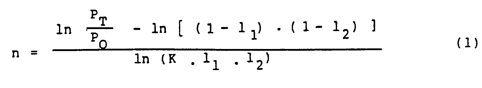
- Because of the characteristics of the couplers, 1, and 1 must be equivalent in order to attain maximum efficiency. By using the formula, if the percentage of power transmitted by the
loop 140 is 100% (K = 1.), the optimal coupling coefficients I, and 12 are .973 to attain the maximum number of useable output signals (which must by definition be at least 1 x 10⁻⁴ of the input level). If 90% of the power is transmitted by the loop (K = .9), the optimum coupling coefficient is .94. A list of the optimum coupling coefficients and maximum number of recirculations for different percentages of power transmitted K by theloop 140 for both the present invention and for the recirculating memory shown in Figure 5 are shown in the chart of Figure 10. - A
typical loop 140 could be a 200 meter length of glass fiber and if the loss of the fiber is about one db per kilometer, the optimum coupling coefficient is about .9575. For convenience, the figure .96 will be used below in describing the operation of the recirculating memory device. Aninput signal 260 of modulated light pulses shown in Figure 9 (and identical to theinput signal 160 shown in Figure 6) is supplied to theinput end 132 of theoptical fiber 130 attime Tl, from alaser light source 150 and amodulator 152. This light will enter the firstoptical coupler 110 through port 110C. Since the coupling efficiency is 96%, 96% of the light will be coupled through theport 110B and lost through theother end 144 of thefiber 112. The remaining 4% of theoriginal input signal 260, which is not coupled, exits thefirst coupler 110 through port 110D, and continues through theoptical fiber 130 into the second coupler 210 through port 210C. Since the coupling coefficiency of the second coupler 210 is also 96%, 96% of the remaining 4% of theoriginal input signal 260 will be coupled and exit the second coupler 210 toport 210b, entering through theoptical fiber 112 into theloop 140, which acts as a delay line. The light not coupled in the second coupler 210 exits through the port 210d through the fiber exit 134, and will be at a power level of .0016 of theoriginal input signal 260. Thisfirst output signal 261, as shown in Figure 9, exits at time T2, which is an instant after Ti, and is thefirst output signal 262 of a series of output signals supplied to the decoder/data processor 154. - After some period of time, which is directly proportional to the length of the
fiber 112 in theloop 140, the light coupled into theloop 140 will leave theloop 140. This light will then enter thefirst coupler 110 throughport 110a, where 96% of it will be coupled toport 110d. This light will enter the second coupler 210 throughport 210c, where 96% of it will be coupled back into theloop 140 and the 4% which is not coupled will leave the coupler 210 through port 210d. This light will be output from thefiber 130 through the fiber exit 134, as thesecond signal 262 of the series of signals at time T3. After thefirst output signal 261 at time T2, the successive output signals occur periodically. Thus, it may be seen that thesecond output signal 262 is an exact reproduction of thefirst signal 261 that was output, although at reduced amplitude, and they both are identical to theinput signal 260, but at a lower amplitude. - As a note of comparison, the
first output signal 261 of Figure 9 is at a useable level, unlike thefirst output signal 161 of Figure 6. Thus, it may be seen that the dual coupler fiber optic recirculating memory of the present invention provides afirst output signal 261 which is at a useable level, eliminating the need for protective circuitry in the decoder/data processor 154. - Each time the light circles the
loop 140, 92.16% of the light will be recirculated back into theloop 140, and 3.84% of the light will be output from the device. About 4% of the light is lost when it exits theother end 144 of thefiber 112, making the output signals shown in Figure 9 decrease at a slightly faster rate than do the output signals of Figure 6. Thus, it may be seen that in order to obtain a series of output pulses all at a useable level, and to prevent the first output pulse from being of a proportionately extremely high level, the trade-off required by the present invention is to reduce the efficiency of operation by about 4% - this decrease in efficiency caused by the light exiting through theend 144 offiber 112. For any input signal, a series of output signals identical to the input signal but with decreasing amplitude will be supplied from the device. - While the successive output signals may differ somewhat in pulse shape due to dispersion, they will be substantially identical, and they will be separated to provide adequate resolution of consecutive output signals as long as the duration of the
input signal 260 supplied to the device is sufficiently shorter than the delay time provided by theloop 140 to compensate for dispersion. Thus, it can be seen that a signal may be modulated onto the light input to the device, and a series of decreasing amplitude output pulses will be periodically provided to the decoder/data processor 154, the length of the period proportional to the length of thefiber 112 in theloop 140. - This feature makes the system highly useful as a recirculating memory device supplying data to a processor, since the series of identical output signals allows the data processor to sample different portions of the data upon successive circulations. In this way, a data processor operating at a slower rate than the device generating the data may be used by utilizing the recirculating memory.
- In Figure 9, for example, during the
first output signal 261, the first data bit may be read by the data processor. During thesecond series 262, the second bit may be read. During thethird series 263, the third bit may be read, and so on. - The device shown in Figure 8 may also be used as a tap delay line transversal filter to pass some frequencies and reject others. A basic optical tap delay line is shown in Figure 7. A
light source 170 injects light into anoptical fiber 172. Thisoptical fiber 172 has fourtaps 180,182,184,186 installed along its length, with thetaps optical fiber 172. Thetaps fiber 172 to their outputs, which are, respectively, outputs 190, 192, 194, 196. - If the
light source 170 provides an input signal which varies as some function of time, the optical tap may be used to filter selected frequencies from the input signal. Thus, by summing theoutputs fiber 172 between thetaps - The recirculating loop device disclosed here may be used as a transversal filter by providing an input signal from the
laser light source 150 and themodulator 152 which varies as some function of time. The period of the fundamental frequency may be set by selecting the length of thefiber 12 in theloop 140 so that its delay time will be equivalent to the period of the fundamental frequency desired. That portion of the input signal corresponding to the fundamental frequency and the harmonics of that frequency will then be passed from the fiber exit 134 to the decoder/data processor 154, but other frequencies will be attenuated, since they do not constructively add at thecouplers 110 and 210, and thus the device may be used to indicate the presence or absence of the fundamental frequency and its harmonics. - The advantages of this device over the Suzaki device are fairly impressive. There are no longer any losses caused by the necessity of having a splice in the loop. Since the presence of a splice causes great losses, the limitation of the Suzaki device is that only a relatively small number of output pulses may be obtained. The device of the present invention, on the other hand, has no loss due to the presence of a splice, and therefore is able to provide a greater number of output pulses of a usable amplitude. This allows a greater difference between processing speed and input speed.
- The second advantage the device of the present invention has over the Suzaki reference is that much higher frequencies may be used, since single mode optical fiber is used rather than the multi-mode fiber of the Suzaki device. This advantage, of course, is also a significant advantage over the coaxial cable and acoustic devices described above. The higher frequencies and lower losses of the device disclosed here enable a recirculating memory device to be used in a system which generates data at such a high rate that a conventional data processor cannot handle it. The accurate transmission of such data is now made possible by this device.
- The advantage the device of the present invention has over the device shown in Figure 5 is that the relatively high level of the first output signal is eliminated, although the trade-off is that the number of useable output signals is reduced somewhat. This enables the data processor used to have a narrower power band, and thus, to be made more accurate. In addition, protective circuitry on the output end is no longer required.
Claims (11)
said fiber optic recirculating memory device being characterized by:

Priority Applications (1)
| Application Number | Priority Date | Filing Date | Title |
|---|---|---|---|
| AT82306164T ATE60144T1 (en) | 1981-12-01 | 1982-11-18 | FIBER OPTIC LOOP MEMORY WITH TWO COUPLERS. |
Applications Claiming Priority (2)
| Application Number | Priority Date | Filing Date | Title |
|---|---|---|---|
| US06/326,215 US4479701A (en) | 1981-12-01 | 1981-12-01 | Dual coupler fiber optic recirculating memory |
| US326215 | 1981-12-01 |
Publications (3)
| Publication Number | Publication Date |
|---|---|
| EP0080841A2 EP0080841A2 (en) | 1983-06-08 |
| EP0080841A3 EP0080841A3 (en) | 1986-06-25 |
| EP0080841B1 true EP0080841B1 (en) | 1991-01-16 |
Family
ID=23271292
Family Applications (1)
| Application Number | Title | Priority Date | Filing Date |
|---|---|---|---|
| EP82306164A Expired - Lifetime EP0080841B1 (en) | 1981-12-01 | 1982-11-18 | Dual coupler fiber optic recirculating memory |
Country Status (11)
| Country | Link |
|---|---|
| US (1) | US4479701A (en) |
| EP (1) | EP0080841B1 (en) |
| JP (1) | JPS58171002A (en) |
| KR (1) | KR880002471B1 (en) |
| AT (1) | ATE60144T1 (en) |
| AU (1) | AU564234B2 (en) |
| BR (1) | BR8206910A (en) |
| CA (1) | CA1194221A (en) |
| DE (1) | DE3280294D1 (en) |
| IL (1) | IL67276A (en) |
| NO (1) | NO824014L (en) |
Cited By (2)
| Publication number | Priority date | Publication date | Assignee | Title |
|---|---|---|---|---|
| CN103149635A (en) * | 2013-03-04 | 2013-06-12 | 东南大学 | Manufacturing method of fixed long-delay optical fiber delay line and optical fiber cutting device |
| CN109074244A (en) * | 2016-03-22 | 2018-12-21 | 利特洛普技术有限公司 | Exercise data storage system and method |
Families Citing this family (39)
| Publication number | Priority date | Publication date | Assignee | Title |
|---|---|---|---|---|
| US4588255A (en) * | 1982-06-21 | 1986-05-13 | The Board Of Trustees Of The Leland Stanford Junior University | Optical guided wave signal processor for matrix-vector multiplication and filtering |
| ATE50071T1 (en) * | 1982-11-12 | 1990-02-15 | Univ Leland Stanford Junior | FIBER OPTIC SWITCH AND DISCREET ADJUSTABLE DELAY LINE. |
| DE3322947A1 (en) * | 1983-06-25 | 1985-01-10 | Standard Elektrik Lorenz Ag, 7000 Stuttgart | TRANSVERSAL FILTER FOR ELECTROMAGNETIC SHAFTS |
| FR2553951B1 (en) * | 1983-10-25 | 1985-12-27 | Thomson Csf | INFORMATION STORAGE DEVICE IN A FIBER OPTIC TRANSMISSION SYSTEM |
| DE3339188A1 (en) * | 1983-10-26 | 1985-05-09 | Heinrich-Hertz-Institut für Nachrichtentechnik Berlin GmbH, 1000 Berlin | OPTICAL RESONATOR WITH A MONOMODE FIBER AS A RESONATOR RING AND USE OF SUCH RESONATORS |
| US4778237A (en) * | 1984-06-07 | 1988-10-18 | The Board Of Trustees Of The Leland Stanford Junior University | Single-mode fiber optic saturable absorber |
| US4815804A (en) * | 1985-02-08 | 1989-03-28 | The Board Of Trustees Of The Leland Stanford Junior University | In-line fiber optic memory and method of using same |
| US4696063A (en) * | 1985-08-30 | 1987-09-22 | Pacific Bell | Optical fiber bandwidth limiting method |
| US4692610A (en) * | 1986-01-30 | 1987-09-08 | Grumman Aerospace Corporation | Fiber optic aircraft load relief control system |
| US4734577A (en) * | 1986-01-30 | 1988-03-29 | Grumman Aerospace Corporation | Continuous strain measurement along a span |
| US4777661A (en) * | 1986-09-22 | 1988-10-11 | Simmonds Precision Products, Inc. | Apparatus and method for self-referencing and multiplexing intensity modulating fiber optic sensors |
| US4859018A (en) * | 1987-06-15 | 1989-08-22 | Northern Telecom Limited | Optical fiber bandwidth limiting |
| US4947693A (en) * | 1987-07-28 | 1990-08-14 | Grumman Aerospace Corporation | Discrete strain sensor |
| US4808999A (en) * | 1988-02-18 | 1989-02-28 | Loral Corp. | Towed decoy with fiber optic link |
| GB8813667D0 (en) * | 1988-06-09 | 1988-07-13 | British Telecomm | Wavelength selective optical waveguide coupler |
| JP2842654B2 (en) * | 1990-02-05 | 1999-01-06 | 日本電信電話株式会社 | Optical elastic store circuit |
| US5253935A (en) * | 1990-05-04 | 1993-10-19 | Raychem Corporation | Couples for terminating optical fiber ends |
| JP3085311B2 (en) * | 1990-05-25 | 2000-09-04 | 日本電信電話株式会社 | FIFO buffer |
| US5185833A (en) * | 1991-02-13 | 1993-02-09 | International Business Machines Corporation | Modular active fiber optic coupler system |
| US5131061A (en) * | 1991-02-13 | 1992-07-14 | International Business Machines Corp. | Modular active fiber optic coupler system |
| US5218652A (en) * | 1991-08-29 | 1993-06-08 | Minnesota Mining And Manufacturing Company | Depolarizer for electromagnetic radiation |
| US5566261A (en) * | 1995-05-25 | 1996-10-15 | Massachusetts Institute Of Technology | Optical memory and data pattern generator |
| GB2321563B (en) * | 1997-01-24 | 1999-04-21 | Plessey Telecomm | Burst mode wavelength manager |
| US6501875B2 (en) * | 2000-06-27 | 2002-12-31 | Oluma, Inc. | Mach-Zehnder inteferometers and applications based on evanescent coupling through side-polished fiber coupling ports |
| US6516114B2 (en) * | 2000-06-27 | 2003-02-04 | Oluma, Inc. | Integration of fibers on substrates fabricated with grooves |
| US6621951B1 (en) * | 2000-06-27 | 2003-09-16 | Oluma, Inc. | Thin film structures in devices with a fiber on a substrate |
| US6597833B1 (en) * | 2000-06-27 | 2003-07-22 | Oluma, Inc. | Wavelength-division multiplexers and demultiplexers based on mach-zehnder interferometers and evanescent coupling |
| US6625349B2 (en) * | 2000-06-27 | 2003-09-23 | Oluma, Inc. | Evanescent optical coupling between a waveguide formed on a substrate and a side-polished fiber |
| US6571035B1 (en) * | 2000-08-10 | 2003-05-27 | Oluma, Inc. | Fiber optical switches based on optical evanescent coupling between two fibers |
| US6621952B1 (en) * | 2000-08-10 | 2003-09-16 | Oluma, Inc. | In-fiber variable optical attenuators and modulators using index-changing liquid media |
| US6542663B1 (en) * | 2000-09-07 | 2003-04-01 | Oluma, Inc. | Coupling control in side-polished fiber devices |
| US7092596B2 (en) * | 2002-04-19 | 2006-08-15 | Raytheon Company | Repetitive waveform generator recirculating delay line |
| US6754417B2 (en) * | 2002-04-24 | 2004-06-22 | Agilent Technologies, Inc. | Optical fiber tap capable of random placement along an optical fiber |
| US8970945B2 (en) | 2012-07-24 | 2015-03-03 | University of Zagreb, Faculty of Electrical Engineering and Computing | Modulation averaging reflectors |
| EP3834019A4 (en) | 2018-08-02 | 2022-05-18 | Lyteloop Technologies, Llc | Apparatus and method for storing wave signals in a cavity |
| RU2754829C1 (en) | 2018-08-10 | 2021-09-07 | ЛАЙТЛУП ТЕКНОЛОДЖИЗ, ЭлЭлСи | System and method for increasing path length of wave signal with using angular multiplexing |
| BR112021004133A8 (en) | 2018-11-05 | 2023-05-09 | Lyteloop Tech Llc | SYSTEMS AND METHODS FOR CONSTRUCTING, OPERATING AND CONTROLLING MULTIPLE AMPLIFIERS, REGENERATORS AND TRANSCEIVERS USING THE COMMON SHARED COMPONENTS |
| CN113804412B (en) * | 2021-07-20 | 2024-05-31 | 广东工业大学 | Micro-chromatic dispersion measuring device of optical fiber device based on annular light path structure |
| CN113804405A (en) * | 2021-08-16 | 2021-12-17 | 广东工业大学 | Micro optical fiber dispersion measuring device based on double-coupler ring optical path structure |
Family Cites Families (5)
| Publication number | Priority date | Publication date | Assignee | Title |
|---|---|---|---|---|
| JPS579041B2 (en) * | 1974-11-29 | 1982-02-19 | ||
| US4159418A (en) * | 1977-06-23 | 1979-06-26 | Hughes Aircraft Company | Delay line encoder-decoder |
| JPS5611432A (en) * | 1979-07-09 | 1981-02-04 | Matsushita Electric Ind Co Ltd | Light delay device |
| US4307933A (en) * | 1980-02-20 | 1981-12-29 | General Dynamics, Pomona Division | Optical fiber launch coupler |
| US4317614A (en) * | 1980-02-20 | 1982-03-02 | General Dynamics, Pomona Division | Fiber optic bus manifold |
-
1981
- 1981-12-01 US US06/326,215 patent/US4479701A/en not_active Expired - Fee Related
-
1982
- 1982-11-16 IL IL67276A patent/IL67276A/en unknown
- 1982-11-18 DE DE8282306164T patent/DE3280294D1/en not_active Expired - Fee Related
- 1982-11-18 EP EP82306164A patent/EP0080841B1/en not_active Expired - Lifetime
- 1982-11-18 AT AT82306164T patent/ATE60144T1/en not_active IP Right Cessation
- 1982-11-23 AU AU90812/82A patent/AU564234B2/en not_active Ceased
- 1982-11-27 JP JP57208369A patent/JPS58171002A/en active Pending
- 1982-11-29 BR BR8206910A patent/BR8206910A/en unknown
- 1982-11-30 NO NO824014A patent/NO824014L/en unknown
- 1982-11-30 CA CA000416685A patent/CA1194221A/en not_active Expired
- 1982-11-30 KR KR8205383A patent/KR880002471B1/en active
Non-Patent Citations (1)
| Title |
|---|
| Electronics Letters, Vol. 16, No. 7, p. 260-261 * |
Cited By (3)
| Publication number | Priority date | Publication date | Assignee | Title |
|---|---|---|---|---|
| CN103149635A (en) * | 2013-03-04 | 2013-06-12 | 东南大学 | Manufacturing method of fixed long-delay optical fiber delay line and optical fiber cutting device |
| CN103149635B (en) * | 2013-03-04 | 2014-06-25 | 东南大学 | Manufacturing method of fixed long-delay optical fiber delay line and optical fiber cutting device |
| CN109074244A (en) * | 2016-03-22 | 2018-12-21 | 利特洛普技术有限公司 | Exercise data storage system and method |
Also Published As
| Publication number | Publication date |
|---|---|
| EP0080841A2 (en) | 1983-06-08 |
| EP0080841A3 (en) | 1986-06-25 |
| NO824014L (en) | 1983-06-02 |
| KR840002530A (en) | 1984-07-02 |
| KR880002471B1 (en) | 1988-11-14 |
| DE3280294D1 (en) | 1991-02-21 |
| BR8206910A (en) | 1983-10-04 |
| US4479701A (en) | 1984-10-30 |
| CA1194221A (en) | 1985-09-24 |
| AU9081282A (en) | 1983-06-09 |
| ATE60144T1 (en) | 1991-02-15 |
| IL67276A (en) | 1987-03-31 |
| JPS58171002A (en) | 1983-10-07 |
| IL67276A0 (en) | 1983-03-31 |
| AU564234B2 (en) | 1987-08-06 |
Similar Documents
| Publication | Publication Date | Title |
|---|---|---|
| EP0080841B1 (en) | Dual coupler fiber optic recirculating memory | |
| EP0078140B1 (en) | Splice-free fiber optic recirculating memory | |
| US4652079A (en) | High speed pulse train generator | |
| US4557552A (en) | Microbend optical fiber tapped delay line | |
| US4693544A (en) | Optical branching device with internal waveguide | |
| AU598129B2 (en) | Optical waveguide with reflection diffraction grating | |
| US4262995A (en) | Planar star coupler device for fiber optics | |
| EP0229456B1 (en) | Molecular bonded fiber optic couplers and method of fabrication | |
| US4566753A (en) | Optical star coupler | |
| JPS6344603A (en) | Optical transmitter | |
| US3967877A (en) | Coupler for coupling optical energy transmitted by optical fiber to optical waveguide and method of manufacture | |
| JPH08262244A (en) | Side-gap mode taper ring for integrated optical waveguide | |
| EP0371675B1 (en) | Non-invasive optical coupler | |
| Hsu et al. | Single-mode coupling between fibers and indiffused waveguides | |
| JPS62291604A (en) | Optical branching/coupling device | |
| Sasaki et al. | Propagation characteristics of optical guided waves in asymmetric branching waveguides | |
| US3887264A (en) | Optical fiber with asymmetric index profile | |
| US4838636A (en) | Optical star coupler | |
| Love et al. | Generalized Fresnel power transmission coefficients for curved graded-index media | |
| Kagami et al. | Multimode power divider using radiation from tight bending waveguide | |
| Abd-Alrahman et al. | Silicon Waveguide Analysis | |
| Ibrahim Fawaz | Silicon Waveguide Analysis | |
| Yoshikawa et al. | Analysis of asymmetric two‐core single‐mode optical fibers for subscriber lines | |
| CA1264582A (en) | Molecular bonded fiber optic couplers and method of fabrication | |
| CA1231566A (en) | Optical guided wave signal processor for matrix- vector multiplication and filtering |
Legal Events
| Date | Code | Title | Description |
|---|---|---|---|
| PUAI | Public reference made under article 153(3) epc to a published international application that has entered the european phase |
Free format text: ORIGINAL CODE: 0009012 |
|
| AK | Designated contracting states |
Designated state(s): AT BE CH DE FR GB IT LI LU NL SE |
|
| PUAL | Search report despatched |
Free format text: ORIGINAL CODE: 0009013 |
|
| AK | Designated contracting states |
Kind code of ref document: A3 Designated state(s): AT BE CH DE FR GB IT LI LU NL SE |
|
| 17P | Request for examination filed |
Effective date: 19861031 |
|
| 17Q | First examination report despatched |
Effective date: 19871229 |
|
| GRAA | (expected) grant |
Free format text: ORIGINAL CODE: 0009210 |
|
| AK | Designated contracting states |
Kind code of ref document: B1 Designated state(s): AT BE CH DE FR GB IT LI LU NL SE |
|
| PG25 | Lapsed in a contracting state [announced via postgrant information from national office to epo] |
Ref country code: SE Effective date: 19910116 Ref country code: NL Effective date: 19910116 Ref country code: LI Effective date: 19910116 Ref country code: CH Effective date: 19910116 Ref country code: BE Effective date: 19910116 Ref country code: AT Effective date: 19910116 |
|
| REF | Corresponds to: |
Ref document number: 60144 Country of ref document: AT Date of ref document: 19910215 Kind code of ref document: T |
|
| ITF | It: translation for a ep patent filed |
Owner name: JACOBACCI & PERANI S.P.A. |
|
| REF | Corresponds to: |
Ref document number: 3280294 Country of ref document: DE Date of ref document: 19910221 |
|
| ET | Fr: translation filed | ||
| REG | Reference to a national code |
Ref country code: CH Ref legal event code: PL |
|
| NLV1 | Nl: lapsed or annulled due to failure to fulfill the requirements of art. 29p and 29m of the patents act | ||
| PLBE | No opposition filed within time limit |
Free format text: ORIGINAL CODE: 0009261 |
|
| STAA | Information on the status of an ep patent application or granted ep patent |
Free format text: STATUS: NO OPPOSITION FILED WITHIN TIME LIMIT |
|
| PG25 | Lapsed in a contracting state [announced via postgrant information from national office to epo] |
Ref country code: LU Free format text: LAPSE BECAUSE OF NON-PAYMENT OF DUE FEES Effective date: 19911130 |
|
| 26N | No opposition filed | ||
| PGFP | Annual fee paid to national office [announced via postgrant information from national office to epo] |
Ref country code: FR Payment date: 19940915 Year of fee payment: 13 |
|
| PGFP | Annual fee paid to national office [announced via postgrant information from national office to epo] |
Ref country code: GB Payment date: 19940928 Year of fee payment: 13 |
|
| PGFP | Annual fee paid to national office [announced via postgrant information from national office to epo] |
Ref country code: DE Payment date: 19941230 Year of fee payment: 13 |
|
| PG25 | Lapsed in a contracting state [announced via postgrant information from national office to epo] |
Ref country code: GB Effective date: 19951118 |
|
| GBPC | Gb: european patent ceased through non-payment of renewal fee |
Effective date: 19951118 |
|
| PG25 | Lapsed in a contracting state [announced via postgrant information from national office to epo] |
Ref country code: FR Effective date: 19960731 |
|
| PG25 | Lapsed in a contracting state [announced via postgrant information from national office to epo] |
Ref country code: DE Effective date: 19960801 |
|
| REG | Reference to a national code |
Ref country code: FR Ref legal event code: ST |