EP0080415B1 - Self-refreshing memory cell - Google Patents
Self-refreshing memory cell Download PDFInfo
- Publication number
- EP0080415B1 EP0080415B1 EP82402116A EP82402116A EP0080415B1 EP 0080415 B1 EP0080415 B1 EP 0080415B1 EP 82402116 A EP82402116 A EP 82402116A EP 82402116 A EP82402116 A EP 82402116A EP 0080415 B1 EP0080415 B1 EP 0080415B1
- Authority
- EP
- European Patent Office
- Prior art keywords
- transistor
- drain
- cell
- floating gate
- voltage
- Prior art date
- Legal status (The legal status is an assumption and is not a legal conclusion. Google has not performed a legal analysis and makes no representation as to the accuracy of the status listed.)
- Expired
Links
- 230000015654 memory Effects 0.000 title claims description 39
- 229910021420 polycrystalline silicon Inorganic materials 0.000 claims description 5
- VYPSYNLAJGMNEJ-UHFFFAOYSA-N Silicium dioxide Chemical compound O=[Si]=O VYPSYNLAJGMNEJ-UHFFFAOYSA-N 0.000 claims description 4
- 235000012239 silicon dioxide Nutrition 0.000 claims description 2
- 239000000377 silicon dioxide Substances 0.000 claims description 2
- 239000004065 semiconductor Substances 0.000 description 4
- 230000003068 static effect Effects 0.000 description 4
- 230000000694 effects Effects 0.000 description 3
- 238000000034 method Methods 0.000 description 3
- 238000013461 design Methods 0.000 description 2
- 238000009792 diffusion process Methods 0.000 description 2
- 230000003014 reinforcing effect Effects 0.000 description 2
- 239000000758 substrate Substances 0.000 description 2
- ZOKXTWBITQBERF-UHFFFAOYSA-N Molybdenum Chemical compound [Mo] ZOKXTWBITQBERF-UHFFFAOYSA-N 0.000 description 1
- 229910052581 Si3N4 Inorganic materials 0.000 description 1
- 229910052782 aluminium Inorganic materials 0.000 description 1
- XAGFODPZIPBFFR-UHFFFAOYSA-N aluminium Chemical compound [Al] XAGFODPZIPBFFR-UHFFFAOYSA-N 0.000 description 1
- 239000003990 capacitor Substances 0.000 description 1
- 239000004020 conductor Substances 0.000 description 1
- 238000010276 construction Methods 0.000 description 1
- 230000008878 coupling Effects 0.000 description 1
- 238000010168 coupling process Methods 0.000 description 1
- 238000005859 coupling reaction Methods 0.000 description 1
- 238000013500 data storage Methods 0.000 description 1
- 230000007423 decrease Effects 0.000 description 1
- 230000001419 dependent effect Effects 0.000 description 1
- 239000003989 dielectric material Substances 0.000 description 1
- 238000009413 insulation Methods 0.000 description 1
- 238000005468 ion implantation Methods 0.000 description 1
- 239000000463 material Substances 0.000 description 1
- 229910052751 metal Inorganic materials 0.000 description 1
- 239000002184 metal Substances 0.000 description 1
- 229910052750 molybdenum Inorganic materials 0.000 description 1
- 239000011733 molybdenum Substances 0.000 description 1
- 229910001120 nichrome Inorganic materials 0.000 description 1
- 238000012856 packing Methods 0.000 description 1
- 229920005591 polysilicon Polymers 0.000 description 1
- 238000012545 processing Methods 0.000 description 1
- 230000008672 reprogramming Effects 0.000 description 1
- 230000004044 response Effects 0.000 description 1
- 229910021332 silicide Inorganic materials 0.000 description 1
- FVBUAEGBCNSCDD-UHFFFAOYSA-N silicide(4-) Chemical compound [Si-4] FVBUAEGBCNSCDD-UHFFFAOYSA-N 0.000 description 1
- HQVNEWCFYHHQES-UHFFFAOYSA-N silicon nitride Chemical compound N12[Si]34N5[Si]62N3[Si]51N64 HQVNEWCFYHHQES-UHFFFAOYSA-N 0.000 description 1
- 238000012546 transfer Methods 0.000 description 1
Images

Classifications
-
- G—PHYSICS
- G11—INFORMATION STORAGE
- G11C—STATIC STORES
- G11C14/00—Digital stores characterised by arrangements of cells having volatile and non-volatile storage properties for back-up when the power is down
-
- H—ELECTRICITY
- H10—SEMICONDUCTOR DEVICES; ELECTRIC SOLID-STATE DEVICES NOT OTHERWISE PROVIDED FOR
- H10B—ELECTRONIC MEMORY DEVICES
- H10B10/00—Static random access memory [SRAM] devices
-
- H—ELECTRICITY
- H10—SEMICONDUCTOR DEVICES; ELECTRIC SOLID-STATE DEVICES NOT OTHERWISE PROVIDED FOR
- H10B—ELECTRONIC MEMORY DEVICES
- H10B10/00—Static random access memory [SRAM] devices
- H10B10/12—Static random access memory [SRAM] devices comprising a MOSFET load element
-
- H—ELECTRICITY
- H10—SEMICONDUCTOR DEVICES; ELECTRIC SOLID-STATE DEVICES NOT OTHERWISE PROVIDED FOR
- H10B—ELECTRONIC MEMORY DEVICES
- H10B10/00—Static random access memory [SRAM] devices
- H10B10/15—Static random access memory [SRAM] devices comprising a resistor load element
Definitions
- This invention relates to a self-refreshing memory cell suitable for use in an integrated circuit with increased packing density over circuits of the prior art, and to its method of operation.
- Bistable memory cells are well known. Such cells are disclosed, for example, in United States Patent No. 3,562,721 to Norman, issued February 9, 1971.
- the Normal cell comprises two cross-coupled bipolar transistors connected in what has now become a standard bistable flip-flop configuration.
- the collector of one bipolar transistor in the cell is connected to the base of the other transistor and the emitters of the two transistors are grounded.
- the collector voltage on that transistor drops thereby turning off the other transistor.
- the collector voltage on the off transistor then rises turning on harder the "on” transistor.
- the state of the cell is changed by pulsing simultaneously the collector of the cross-coupled transistor and a selected switching transistor.
- the state of the cell is sensed by determining the voltages on the collectors of the two transistors.
- Publication E-A-28 935 discloses an electronic memory which exhibits the features set forth in the pre-characterizing portion of patent claim 1. The higher potential is applied to the control gate of the transistor; another publication GB-A-2 000 407 applies the higher potential to the power supply.
- This invention provides structures which resemble conventional cross-coupled flip-flops. However, contrary to such flip-flops, the coupling in the flip-flops of this invention is AC rather than DC.
- the flip-flops of this invention may be written into and read from in a conventional manner. However, since the drain voltage on the active element which is off is always in the same direction as for writing, drain disturb reinforces writing assuming that the volatile information stored in the cell is the same as the non-volatile state of the cell. Should these two states be different, then a normal disturb will degrade, rather than reinforce, writing.
- bistable memory cell 10 comprises two MOS transistors M, and M 2 .
- M, and M 2 are preferably N-channel devices although these devices could also be P-channel with appropriate changes in the polarities of the voltages.
- M has its source grounded and its drain 11-1 connected to one terminal of resistor R i , the other terminal of which is connected to power supply V cc .
- a gate 11 is separate by insulation from an underlying floating gate 16.
- One portion of floating gate 16 is separated from the drain of M 2 by means of a thin tunnel oxide, typically from 500 to 2000 nm (50 to 200 angstroms) thick, above a portion of the drain of transistor M 2 .
- the gate 11 of transistor M is connected at node 14 to the gate 12 of transistor M 2 and also to voltage source V, by means of lead 17.
- Transistor M 2 has its source grounded and its drain 12-1 connected to one terminal of resistor R 2 , the other terminal of which is also connected to voltage source V cc .
- Floating gate 15 is sandwiched between gate 12 and the channel region of transistor M 2 but is insulated from both gate 12 and the channel region by dielectric. One portion of floating gate 15 is separated from the drain of transistor M, by means of a thin tunnel oxide (500-2000 nm) over a portion of the drain.
- an input signal Y is transmitted to node 18 between resistor R, and the drain of transistor M, through an MOS switching transistor 13 of conventional design.
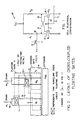
- Figure 2 shows in top view the layout of one embodiment of the circuit shown schematically in Figure 1.
- FIG 2 portions of the layout corresponding to circuit components in Figure 1 are numbered identically.
- Ground in Figure 1 is shown in Figure 2 as a common source diffusion labelled V ss .
- the drain regions of the two transistors M 1 and M 2 are shown in Figure 2 as regions 11-1 and 12-1, respectively.
- the gates 11 and 12 of transistors M 1 and M 2 in Figure 1, respectively, are shown in Figure 2a as a common conductive line 14 with regions 11 and 12 overlying the corresponding channel regions of transistors M 1 and M 2 so as to act as the gate electrodes.
- the drains of transistors M 1 and M 2 are formed by diffusion or by ion-implantation using well-known techniques and extend, in a well-known manner, to contact resistors R 1 and R 2 respectively.
- Resistors R 1 and R 2 can be formed in any one of several ways and can comprise, for example, deposited resistors such as of polysilicon or nichrome on the top surface of the device insulated from the underlying substrate by dielectric or diffused resistors within the semiconductor structure itself or active load devices of well-known construction.
- External signals on lead Y accessed through transistor 13 to the cell, read and write the flip-flop in a conventional manner.
- a volatile memory is one which loses the information stored therein immediately upon loss of power.
- a non-volatile memory is one which retains the information stored therein despite the loss of power.
- memory cell 10 is capable of storing both volatile and non-volatile information.
- the storage in a volatile manner of a logical one within memory cell 10 of Figure 1 will correspond to transistor M 1 nonconducting and transistor M 2 conducting.
- the storage in a volatile manner of a logical zero within memory cell 10 will correspond to transistor M 1 conducting and transistor M, nonconducting.
- the storage in a non-volatile manner of a logical one within memory cell 10 corresponds to a threshold voltage of transistor M 2 which is less than the threshold voltage of transistor M i
- the storage in a non-volatile manner of a logical zero corresponds to a threshold voltage of transistor M 2 which is greater than the threshold voltage of transistor M 1 .
- a data input signal is provided on lead Y ( Figure 1) through gating transistor 13 to node 18.
- This data input signal is high and is approximately equal to V cc (e.g. both the high data input signal and V cc are approximately 5 volts) if a one is to be written into cell 10 and is low (e.g. approximately 0 volts) if a zero is to be written into cell 10.
- the data input signal on node 18 is capacitively coupled to floating gate 15 of transistor M 2 .
- the low voltage on drain 11-1 is capacitively coupled through tunnel oxide to floating gate 15 reinforcing the turning off of M 2 . Accordingly, transistor M 2 remains off and transistor M 1 remains on after removal of the low data input voltage from lead Y. Thus, with the application of a low data input voltage on node 18 from lead Y through gating transistor 13, a logical zero is written into cell 10.
- a high voltage is applied on lead Y to node 18.
- V 1 normal gate voltage
- the high voltage on node 18 is capacitively caoupled through tunnel oxide to floating gate 15, thus increasing the gate potential of transistor M 2 , causing transistor M 2 to conduct.
- transistor M 2 With transistor M 2 conducting, the voltage on drain 12-1 is substantially ground. This low voltage on drain 12-1 is capacitively coupled through tunnel oxide to floating gate 16, thus causing a low gate voltage on transistor M i , thus causing transistor M 1 to remain off.
- transistor M 1 With transistor M 1 turned off, the voltage on node 18 remains substantially V cc , even in the absence of the high data input signal from lead Y. Thus, transistor M 2 remains on and transistor M 1 remains off after the removal of the high data input signal from node 18. In this manner, a logical one is stored in a volatile manner in cell 10.
- the state of the data stored in memory cell 10 in a volatile manner is determined by the voltage on node 18.
- node 18 is connected through gating transistor 13 to lead Y which in turn is connected to a suitable sense amplifier of well known design (not shown).
- the sense amplifier is capable of providing an output signal corresponding to a logical 1 when node 18 is high (transistor M 1 nonconducting and transistor M 2 conducting), and an output signal corresponding to a logical low when the voltage on node 18 is low (transistor M, conducting and transistor M 2 nonconducting).
- Non-volatile writing into the bistable cell 10 of Figure 1 takes place as follows.
- V cc is raised to the writing voltage V w (typically 15 ⁇ 20 volts)
- the state of the cell i.e. transistor M 1 conducting and transistor M 2 nonconducting or vice versa
- V w typically 15 ⁇ 20 volts
- the state of the cell i.e. transistor M 1 conducting and transistor M 2 nonconducting or vice versa
- V w typically 15 ⁇ 20 volts
- the drain 11-1 of transistor M 1 will then be high (at V w ), causing electrons to tunnel from the floating gate 15 of transistor M 2 to the drain 11-1 of transistor M 1 , thereby lowering the threshold voltage of transistor M 2 .
- Transistor M 2 is conducting and therefore the drain 12-1 of transistor M 2 is low. Thus no electrons will tunnel into or out of floating gate 16, and the threshold voltage of transistor M 1 is not affected. There is no tunnelling within the active structures of transistors M 1 and M 2 but rather only in the external tunnelling regions associated with the drains of these two transistors, because these are the only two regions of the device in which the oxide is thin enough (500-2000 nm) to permit tunnelling.
- the threshold voltage V 12 of transistor M 2 is programmed to be less than the threshold voltage V t1 of transistor M, which, as previously mentioned, corresponds to the non-volatile storage of a logical one in cell 10.
- the data stored in a non-volatile manner determines the initial state of cell 10. For example, if a logical 1 is stored in a non-volatile manner in cell 10 such that the threshold voltage of transistor M 2 is less than the threshold voltage of transistor M 1 , upon the application of V cc (approximately 5 volts) and gate voltage V, (also approximately 5 volts) to gates 11 and 12 of transistors M 1 and M 2 respectively, transistor M 2 will turn on first, thereby lowering the voltage of drain 12-1 to ground.
- This low voltage on drain 12-1 is capacitively coupled through tunnel oxide to floating gate 16 of transistor M i , thus causing transistor M 1 to remain off.
- transistor M 2 is on and transistor M 1 is off, corresponding to a logical one.
- transistor M 1 will turn on first, thereby lowering the voltage on drain 11-1 to ground.
- This low voltage on drain 11-1 is capacitively coupled through tunnel oxide to floating gate 15 of transistor M 2 , thus preventing transistor M 2 from turning on, resulting in the flip-flop comprising transistors M i and M 2 being set to a logical zero.
- Erasure of the data stored in cell 10 in a non-volatile manner is performed by increasing V 1 applied to gates 11 and 12 of transistors M 1 and M 2 , respectively, to the erase voltage V E of approximately 20-25 volts. If V cc is five volts, then both M 1 and M 2 turn on, thereby ensuring equal drain voltages on these two devices. Tunnelling occurs such that the same amount of charge is stored on each floating gate and the circuit is balanced upon completion of erase. Erase, which corresponds to the tunnelling of electrons from the drains 11-1 and 12-1 of the transistors M 1 and M 2 , respectively, to the floating gates 15 and 16, respectively, results in an increase in the threshold voltages of transistors M 1 and M 2 . The actual threshold voltages of M, and M 2 are varied by varying the magnitude and duration of the erase signal. It is not required to drive the threshold voltages of transistors M, and M 2 into heavy enhancement since the cell 10 is capable of operating in the depletion mode.
- Figure 3 illustrates the floating gate voltage with respect to time for different levels of drain voltages.
- the effective threshold voltage of the device remains constant for in excess of 10 9 seconds which corresponds to about 33 years.
- the voltage on the floating gate decays only by about 0.3 volts. Accordingly, this device has the ability to hold charge over an extremely long time.
- the charge can be easily erased by merely raising the voltage on lead 17 to a high level. The erasure occurs in a fraction of a second (typically about 100 milliseconds).
- the cell of this invention may be used in two modes, a non-volatile mode wherein the cell comprises a non-volatile static RAM and a volatile mode in which the flip-flop operates as a volatile static RAM cell.
- volatile data can be stored non-volatily provided the cell has already been erased.
- V cc is raised to V w for a few milliseconds.
- the volatile data in the cell is converted to non-volatile data through the tunnelling of electrons in the manner described above.
- the cell's floating gates therefore retain in a non-volatile manner the electrons indicative of the volatile state of the cell prior to powering down.
- the cell can hold this data for many years, if necessary.
- the data transfer to non-volatile storage occurs simultaneously for all bits in the memory.
- Suitable circuitry can be utilized for determining when power-down is about to occur.
- circuitry can be used which determines when V cc drops to a predetermined level below normal.
- a suitable signal may be provided by the system (such as a computer system, for example) in which the memory cell of this invention is utilized, thus instructing memory cell 10 to write the volatile data in the cell in a non-volatile manner, as described above.
- the writing voltage V w may be provided during power-down by a capacitor, for example, which has been charged during normal powered operation of the memory cell 10.
- each cell can be operated as a volatile static memory cell in the standard manner but additionally can have stored on the floating gates of each cell a bit of data corresponding to a different state (for example, "bootstrap" data to be utilized upon initialization or power-up of the device).
- the cell is then operated by ensuring that the drive voltages used to operate the cell in its volatile storage mode are sufficient to overcome the non-volatile information stored in the cell.
- V 1 the gate voltage on lead 17
- V l will have little effect on floating gate 16 because this floating gate is connected through tunnel oxide to a high potential on the drain 12-1 of transistor M 2 and an increase in the voltage V 1 merely reduces the difference between the potential on floating gate 16 and V cc .
- the normal disturbing voltages are in such a direction as to enhance the storage of information in the cell rather than degrade the storage of information.
- the non-volatile bit is opposite to the volatile bit, the non- volatile bit state is degraded rather than enhanced by positive disturb voltages on V cc .
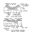
- Figure 4 illustrates in cross section a semiconductor device particularly suited for implementing the structure shown in Figure 1.
- P-type substrate typically ⁇ 100> material with a resistivity of 2-50 ⁇ -cm
- a gate oxide Formed over the surface of the active region of the device is a gate oxide and formed over the gate oxide is a floating gate of a conductive material such as doped polycrystalline silicon or molybdenum.
- dielectric typically silicon dioxide or silicon nitride
- the control gate is again formed of doped polycrystalline silicon, a silicide or selected metal such as aluminum and is capacitively coupled to the floating gate.
- the tunnelling oxide portion is formed directly over the drain such that electrons can tunnel in response to the proper voltages applied to the drain and the floating gate from one to the other.
- a control gate typically formed of doped polycrystalline silicon. This control gate is capacitively coupled to the floating gate so as to control the potential of the floating gate.
Landscapes
- Non-Volatile Memory (AREA)
- Semiconductor Memories (AREA)
Description
- This invention relates to a self-refreshing memory cell suitable for use in an integrated circuit with increased packing density over circuits of the prior art, and to its method of operation.
- Bistable memory cells are well known. Such cells are disclosed, for example, in United States Patent No. 3,562,721 to Norman, issued February 9, 1971. The Normal cell comprises two cross-coupled bipolar transistors connected in what has now become a standard bistable flip-flop configuration. The collector of one bipolar transistor in the cell is connected to the base of the other transistor and the emitters of the two transistors are grounded. When one transistor turns on, the collector voltage on that transistor drops thereby turning off the other transistor. The collector voltage on the off transistor then rises turning on harder the "on" transistor. The state of the cell is changed by pulsing simultaneously the collector of the cross-coupled transistor and a selected switching transistor. The state of the cell is sensed by determining the voltages on the collectors of the two transistors.
- Since the disclosure of this long established cell, new bistable cells have appeared, including cells using a charge stored at the interface between two dissimilar dielectrics (see, for example, U.S. Patent No. 3,641,512 issued February 8, 1972 on an invention of Frohman-Bentchkowsky) and cells using so-called "floating gates" which are conductive gates insulated from the active components of the transistor by dielectric. The charge on the floating gate is often controlled by controlling the potential on an overlying word line in such a manner as to either draw a charge from an underlying source to the floating gate or expell charge from the floating gate to the source. Such devices, often making use of electron tunnelling through a thin dielectric, are described, for example, in an article entitled "Low Power EEPROM Can Be Reprogrammed Fast", published in Electronics, July 31, 1980, by Shelton. The EEPROM, short for "Electrically Erasable Programmable Read Only Memory", has distinct advantages over the prior art memories in that the EEPROM can be erased by programming internal to the chip whereas the standard EPROM is erasable only by UV light from an external source. In addition, the EEPROM lends itself to rapid reprogramming in a simple manner with portable equipment.
- Publication E-A-28 935 discloses an electronic memory which exhibits the features set forth in the pre-characterizing portion of
patent claim 1. The higher potential is applied to the control gate of the transistor; another publication GB-A-2 000 407 applies the higher potential to the power supply. - Both said publications provide data storage in volatile or non-volatile manner. However, data stored in non-volatile modus is the opposite to data stored in volatile modus. Information must be recorded as to the manner in which the data was stored in order to know whether data upon retrieval is or is not to be inverted.
- The present invention overcomes this disadvantage by the features set forth in the characterizing portion of
patent claim 1. Dependent claims 2 through 4 define preferred details of the concept of the invention. - This invention provides structures which resemble conventional cross-coupled flip-flops. However, contrary to such flip-flops, the coupling in the flip-flops of this invention is AC rather than DC. The flip-flops of this invention may be written into and read from in a conventional manner. However, since the drain voltage on the active element which is off is always in the same direction as for writing, drain disturb reinforces writing assuming that the volatile information stored in the cell is the same as the non-volatile state of the cell. Should these two states be different, then a normal disturb will degrade, rather than reinforce, writing.
- This invention will be more fully understood in light of the following description taken together with the drawings.
-
- Figure 1 shows the circuit schematic of a cell of this invention;
- Figure 2 shows a top view of the integrated circuit semiconductor implementation of the cross-coupled structure shown schematically in Figure 1;
- Figure 3 shows graphically an example of the change in threshold voltage with time for the structure of this invention;
- Figures 4 and 5 illustrate in cross-section the floating gate and tunnel oxide structures of a type useful in the semiconductor integrated circuit implementations of the circuits of this invention.
- This invention will be described in conjunction with a specific embodiment. It should be understood, however, that this description is illustrative only and is not meant to limit the scope of the invention.
- As shown in Figure 1,
bistable memory cell 10 comprises two MOS transistors M, and M2. M, and M2 are preferably N-channel devices although these devices could also be P-channel with appropriate changes in the polarities of the voltages. M, has its source grounded and its drain 11-1 connected to one terminal of resistor Ri, the other terminal of which is connected to power supply Vcc. A gate 11 is separate by insulation from an underlyingfloating gate 16. One portion offloating gate 16 is separated from the drain of M2 by means of a thin tunnel oxide, typically from 500 to 2000 nm (50 to 200 angstroms) thick, above a portion of the drain of transistor M2. The gate 11 of transistor M, is connected atnode 14 to thegate 12 of transistor M2 and also to voltage source V, by means oflead 17. - Transistor M2 has its source grounded and its drain 12-1 connected to one terminal of resistor R2, the other terminal of which is also connected to voltage source Vcc. Floating gate 15 is sandwiched between
gate 12 and the channel region of transistor M2 but is insulated from bothgate 12 and the channel region by dielectric. One portion offloating gate 15 is separated from the drain of transistor M, by means of a thin tunnel oxide (500-2000 nm) over a portion of the drain. - In the operation of the circuit of Figure 1, an input signal Y is transmitted to
node 18 between resistor R, and the drain of transistor M, through anMOS switching transistor 13 of conventional design. - Figure 2 shows in top view the layout of one embodiment of the circuit shown schematically in Figure 1. In Figure 2, portions of the layout corresponding to circuit components in Figure 1 are numbered identically. Ground in Figure 1 is shown in Figure 2 as a common source diffusion labelled Vss. The drain regions of the two transistors M1 and M2 are shown in Figure 2 as regions 11-1 and 12-1, respectively. The
gates 11 and 12 of transistors M1 and M2 in Figure 1, respectively, are shown in Figure 2a as a commonconductive line 14 withregions 11 and 12 overlying the corresponding channel regions of transistors M1 and M2 so as to act as the gate electrodes. The drains of transistors M1 and M2 are formed by diffusion or by ion-implantation using well-known techniques and extend, in a well-known manner, to contact resistors R1 and R2 respectively. Resistors R1 and R2 can be formed in any one of several ways and can comprise, for example, deposited resistors such as of polysilicon or nichrome on the top surface of the device insulated from the underlying substrate by dielectric or diffused resistors within the semiconductor structure itself or active load devices of well-known construction. External signals on lead Y, accessed throughtransistor 13 to the cell, read and write the flip-flop in a conventional manner. - Two types of memories are commonly employed-volatile and non-volatile. A volatile memory is one which loses the information stored therein immediately upon loss of power. A non-volatile memory is one which retains the information stored therein despite the loss of power. As will be seen shortly,
memory cell 10 is capable of storing both volatile and non-volatile information. - In describing the operation of
memory cell 10 in this specification, certain conventions will be adopted. Thus, the storage in a volatile manner of a logical one withinmemory cell 10 of Figure 1 will correspond to transistor M1 nonconducting and transistor M2 conducting. Similarly, the storage in a volatile manner of a logical zero withinmemory cell 10 will correspond to transistor M1 conducting and transistor M, nonconducting. The storage in a non-volatile manner of a logical one withinmemory cell 10 corresponds to a threshold voltage of transistor M2 which is less than the threshold voltage of transistor Mi, and the storage in a non-volatile manner of a logical zero corresponds to a threshold voltage of transistor M2 which is greater than the threshold voltage of transistor M1. These conventions are summarized in Table I (wherein Vt represents threshold voltage).
- The operation of the
memory cell 10 as a volatile RAM is as follows. A data input signal is provided on lead Y (Figure 1) throughgating transistor 13 tonode 18. This data input signal is high and is approximately equal to Vcc (e.g. both the high data input signal and Vcc are approximately 5 volts) if a one is to be written intocell 10 and is low (e.g. approximately 0 volts) if a zero is to be written intocell 10. The data input signal onnode 18 is capacitively coupled to floatinggate 15 of transistor M2. - If the data input signal on
node 18 is low, and if a normal gate voltage V1, typically 5 volts, is applied togates 11 and 12 of transistors M1 and M2 respectively, the voltages ongate 12 and floatinggate 15 of transistor M2 are insufficient to turn on transistor M2, thereby causing the voltage on drain 12-1 of transistor M2 to be substantially equal to Vcc. This high voltage on drain 12-1 is capacitively coupled through tunnel oxide to floatinggate 16, thus increasing the gate potential of transistor M1 and thus, together with the low signal voltage onnode 18, causing transistor M1 to conduct. With transistor M1 conducting, the voltage on drain 11-1 is essentially ground. The low voltage on drain 11-1 is capacitively coupled through tunnel oxide to floatinggate 15 reinforcing the turning off of M2. Accordingly, transistor M2 remains off and transistor M1 remains on after removal of the low data input voltage from lead Y. Thus, with the application of a low data input voltage onnode 18 from lead Y through gatingtransistor 13, a logical zero is written intocell 10. - In a similar manner, if it is desired to store in a volatile manner a logical 1 within
memory cell 10, a high voltage is applied on lead Y tonode 18. With a normal gate voltage V1 of approximately 5 volts applied togates 11 and 12 of transistors M, and M2 respectively, the high voltage onnode 18 is capacitively caoupled through tunnel oxide to floatinggate 15, thus increasing the gate potential of transistor M2, causing transistor M2 to conduct. With transistor M2 conducting, the voltage on drain 12-1 is substantially ground. This low voltage on drain 12-1 is capacitively coupled through tunnel oxide to floatinggate 16, thus causing a low gate voltage on transistor Mi, thus causing transistor M1 to remain off. With transistor M1 turned off, the voltage onnode 18 remains substantially Vcc, even in the absence of the high data input signal from lead Y. Thus, transistor M2 remains on and transistor M1 remains off after the removal of the high data input signal fromnode 18. In this manner, a logical one is stored in a volatile manner incell 10. - The state of the data stored in
memory cell 10 in a volatile manner is determined by the voltage onnode 18. To readcell 10,node 18 is connected through gatingtransistor 13 to lead Y which in turn is connected to a suitable sense amplifier of well known design (not shown). The sense amplifier is capable of providing an output signal corresponding to a logical 1 whennode 18 is high (transistor M1 nonconducting and transistor M2 conducting), and an output signal corresponding to a logical low when the voltage onnode 18 is low (transistor M, conducting and transistor M2 nonconducting). - In the volatile operation of
memory cell 10, the voltages applied tonode 18 andnode 14 are not sufficiently high to cause electrons to tunnel through the tunnel oxide between drain 11-1 and floatinggate 15, or between drain 12-1 and floatinggate 16. The situation is different, however, when information is to be stored inmemory cell 10 in a non-volatile manner. - Non-volatile writing into the
bistable cell 10 of Figure 1 takes place as follows. When Vcc is raised to the writing voltage Vw (typically 15―20 volts), the state of the cell (i.e. transistor M1 conducting and transistor M2 nonconducting or vice versa) is written into the cell ina non-volatile manner by the use of floatinggates cell 10 is programmed high (logical one) in a volatile manner such that transistor M1 is off and transistor M2 is on. The gate voltage V1 is 5 volts. The drain 11-1 of transistor M1 will then be high (at Vw), causing electrons to tunnel from the floatinggate 15 of transistor M2 to the drain 11-1 of transistor M1, thereby lowering the threshold voltage of transistor M2. Transistor M2 is conducting and therefore the drain 12-1 of transistor M2 is low. Thus no electrons will tunnel into or out of floatinggate 16, and the threshold voltage of transistor M1 is not affected. There is no tunnelling within the active structures of transistors M1 and M2 but rather only in the external tunnelling regions associated with the drains of these two transistors, because these are the only two regions of the device in which the oxide is thin enough (500-2000 nm) to permit tunnelling. Thus, the threshold voltage V12 of transistor M2 is programmed to be less than the threshold voltage Vt1 of transistor M, which, as previously mentioned, corresponds to the non-volatile storage of a logical one incell 10. - In a similar manner, if
cell 10 is programmed low in a volatile manner such that transistor M1 is on and transistor M2 is off, when Vcc is raised to the writing voltage Vw, drain 12-1 is high (Vw), thus causing electrons to tunnel from floatinggate 16 of transistor M1 to the drain 12-1 of transistor M2, thereby lowering the threshold voltage of transistor M,. Transistor M1 is conducting and the drain 11-1 of transistor M1 is low. Thus no electrons will tunnel into or out of floatinggate 15, and the threshold voltage of transistor M2 is not affected. Thus, the threshold voltage of transistor M1 is programmed to be less than the threshold voltage of transistor M2 which, as previously mentioned, corresponds to the nonvolatile storage of a logical zero incell 10. - Once data has been stored in a non-volatile manner in
memory cell 10, upon normal power-up ofmemory cell 10 by the application of Vcc and V, to the circuit, the data stored in a non-volatile manner determines the initial state ofcell 10. For example, if a logical 1 is stored in a non-volatile manner incell 10 such that the threshold voltage of transistor M2 is less than the threshold voltage of transistor M1, upon the application of Vcc (approximately 5 volts) and gate voltage V, (also approximately 5 volts) togates 11 and 12 of transistors M1 and M2 respectively, transistor M2 will turn on first, thereby lowering the voltage of drain 12-1 to ground. This low voltage on drain 12-1 is capacitively coupled through tunnel oxide to floatinggate 16 of transistor Mi, thus causing transistor M1 to remain off. Thus, transistor M2 is on and transistor M1 is off, corresponding to a logical one. In a similar fashion, if a logical 0 is stored in a non-volatile manner inmemory cell 10 such that the threshold voltage of transistor M1 is less than the threshold voltage of transistor M2, upon power-up, transistor M1 will turn on first, thereby lowering the voltage on drain 11-1 to ground. This low voltage on drain 11-1 is capacitively coupled through tunnel oxide to floatinggate 15 of transistor M2, thus preventing transistor M2 from turning on, resulting in the flip-flop comprising transistors Mi and M2 being set to a logical zero. - Erasure of the data stored in
cell 10 in a non-volatile manner is performed by increasing V1 applied togates 11 and 12 of transistors M1 and M2, respectively, to the erase voltage VE of approximately 20-25 volts. If Vcc is five volts, then both M1 and M2 turn on, thereby ensuring equal drain voltages on these two devices. Tunnelling occurs such that the same amount of charge is stored on each floating gate and the circuit is balanced upon completion of erase. Erase, which corresponds to the tunnelling of electrons from the drains 11-1 and 12-1 of the transistors M1 and M2, respectively, to the floatinggates cell 10 is capable of operating in the depletion mode. - Since the floating
gates lead 17 to a high level. The erasure occurs in a fraction of a second (typically about 100 milliseconds). - The cell of this invention, therefore, may be used in two modes, a non-volatile mode wherein the cell comprises a non-volatile static RAM and a volatile mode in which the flip-flop operates as a volatile static RAM cell. However if desired, volatile data can be stored non-volatily provided the cell has already been erased. To do this, prior to powering down, Vcc is raised to Vw for a few milliseconds. The volatile data in the cell is converted to non-volatile data through the tunnelling of electrons in the manner described above. The cell's floating gates therefore retain in a non-volatile manner the electrons indicative of the volatile state of the cell prior to powering down. As shown in Figure 3, the cell can hold this data for many years, if necessary. As a feature of this invention, the data transfer to non-volatile storage occurs simultaneously for all bits in the memory.
- Suitable circuitry (not shown) can be utilized for determining when power-down is about to occur. For example, circuitry can be used which determines when Vcc drops to a predetermined level below normal. Alternatively, a suitable signal may be provided by the system (such as a computer system, for example) in which the memory cell of this invention is utilized, thus instructing
memory cell 10 to write the volatile data in the cell in a non-volatile manner, as described above. The writing voltage Vw may be provided during power-down by a capacitor, for example, which has been charged during normal powered operation of thememory cell 10. - As an additional feature of this invention, two bits may be stored in each cell, one comprising a volatile storage and the other a non-volatile storage. Thus, the cell can be operated as a volatile static memory cell in the standard manner but additionally can have stored on the floating gates of each cell a bit of data corresponding to a different state (for example, "bootstrap" data to be utilized upon initialization or power-up of the device). The cell is then operated by ensuring that the drive voltages used to operate the cell in its volatile storage mode are sufficient to overcome the non-volatile information stored in the cell.
- The enhancement of the state of the cell due to a disturb voltage is illustrated by assuming M, to be on and M2 to be off. Of importance, most voltage disturbances encountered in memory devices such as the
memory cell 10 of this invention are sudden increases in voltage, rather than decreases in voltage. When M2 is off, the voltage on drain 12-1 of transistor M2 is high, approximately Vcc, while the voltage on the drain 11-1 of transistor M, is low, approximately ground. Should Vcc be driven high by a disturbance, the effect is to remove electrons from floatinggate 16, thereby turning on transistor M, harder and reinforcing the state of the circuit. Floatinggate 15 is not affected because it is connected through tunnel oxide to the drain 11-1 of transistor M, which is substantially at ground. Should V1 (the gate voltage on lead 17) go substantially positive, the effect is to draw further electrons onto floatinggate 15, thereby further turning off transistor M2. Vl will have little effect on floatinggate 16 because this floating gate is connected through tunnel oxide to a high potential on the drain 12-1 of transistor M2 and an increase in the voltage V1 merely reduces the difference between the potential on floatinggate 16 and Vcc. Thus, it is seen that the normal disturbing voltages are in such a direction as to enhance the storage of information in the cell rather than degrade the storage of information. Of course, if the non-volatile bit is opposite to the volatile bit, the non- volatile bit state is degraded rather than enhanced by positive disturb voltages on Vcc. - Figure 4 illustrates in cross section a semiconductor device particularly suited for implementing the structure shown in Figure 1. P-type substrate (typically <100> material with a resistivity of 2-50 Ω-cm) has formed in it N+ source and drain regions using well-known processing techniques. Formed over the surface of the active region of the device is a gate oxide and formed over the gate oxide is a floating gate of a conductive material such as doped polycrystalline silicon or molybdenum. On top of the floating gate is formed dielectric (typically silicon dioxide or silicon nitride) and on top of this dielectric is formed a control gate. The control gate is again formed of doped polycrystalline silicon, a silicide or selected metal such as aluminum and is capacitively coupled to the floating gate. As shown in Figure 5b, the tunnelling oxide portion is formed directly over the drain such that electrons can tunnel in response to the proper voltages applied to the drain and the floating gate from one to the other. Overlying the floating gate but separated therefrom by dielectric is a control gate typically formed of doped polycrystalline silicon. This control gate is capacitively coupled to the floating gate so as to control the potential of the floating gate.
- Other embodiments of this invention will be obvious to those skilled in the art in view of this disclosure.
Claims (4)
Applications Claiming Priority (4)
| Application Number | Priority Date | Filing Date | Title |
|---|---|---|---|
| US324343 | 1981-11-23 | ||
| US06/324,343 US4423491A (en) | 1981-11-23 | 1981-11-23 | Self-refreshing memory cell |
| US324344 | 1981-11-23 | ||
| US06/324,344 US4435786A (en) | 1981-11-23 | 1981-11-23 | Self-refreshing memory cell |
Related Child Applications (1)
| Application Number | Title | Priority Date | Filing Date |
|---|---|---|---|
| EP88118696.9 Division-Into | 1982-11-22 |
Publications (3)
| Publication Number | Publication Date |
|---|---|
| EP0080415A2 EP0080415A2 (en) | 1983-06-01 |
| EP0080415A3 EP0080415A3 (en) | 1985-10-09 |
| EP0080415B1 true EP0080415B1 (en) | 1990-10-10 |
Family
ID=26984408
Family Applications (1)
| Application Number | Title | Priority Date | Filing Date |
|---|---|---|---|
| EP82402116A Expired EP0080415B1 (en) | 1981-11-23 | 1982-11-22 | Self-refreshing memory cell |
Country Status (3)
| Country | Link |
|---|---|
| EP (1) | EP0080415B1 (en) |
| CA (1) | CA1189972A (en) |
| DE (1) | DE3280258D1 (en) |
Family Cites Families (3)
| Publication number | Priority date | Publication date | Assignee | Title |
|---|---|---|---|---|
| GB2000407B (en) * | 1977-06-27 | 1982-01-27 | Hughes Aircraft Co | Volatile/non-volatile logic latch circuit |
| GB2058451B (en) * | 1979-09-13 | 1983-03-16 | Plessey Co Ltd | Semiconductor memory device |
| GB2063601B (en) * | 1979-11-12 | 1984-02-29 | Hughes Microelectronics Ltd | Non-volatile semiconductor memory circuits |
-
1982
- 1982-11-22 CA CA000416051A patent/CA1189972A/en not_active Expired
- 1982-11-22 DE DE8282402116T patent/DE3280258D1/en not_active Expired - Fee Related
- 1982-11-22 EP EP82402116A patent/EP0080415B1/en not_active Expired
Also Published As
| Publication number | Publication date |
|---|---|
| EP0080415A2 (en) | 1983-06-01 |
| DE3280258D1 (en) | 1990-11-15 |
| CA1189972A (en) | 1985-07-02 |
| EP0080415A3 (en) | 1985-10-09 |
Similar Documents
| Publication | Publication Date | Title |
|---|---|---|
| US4435786A (en) | Self-refreshing memory cell | |
| US4907198A (en) | Semiconductor memory device | |
| EP0467928B1 (en) | Improved novram cell using two differential, decouplable nonvolatile memory elements | |
| US4128773A (en) | Volatile/non-volatile logic latch circuit | |
| EP0295935B1 (en) | Electrically erasable programmable read only memory | |
| US4999812A (en) | Architecture for a flash erase EEPROM memory | |
| US5065201A (en) | Semiconductor memory device | |
| US4616245A (en) | Direct-write silicon nitride EEPROM cell | |
| JPH06507039A (en) | Non-volatile programmable/erasable interconnect cells | |
| EP0083386A2 (en) | Memory cell | |
| JPS62117196A (en) | Electrically erasable programmable memory cell and its fabrication method | |
| JPH0143400B2 (en) | ||
| EP0098654A2 (en) | Non-volatile static random-access memory cell | |
| US4479203A (en) | Electrically erasable programmable read only memory cell | |
| US5251171A (en) | Method of operating a semiconductor memory device | |
| US5905675A (en) | Biasing scheme for reducing stress and improving reliability in EEPROM cells | |
| JPS63188896A (en) | Nonvolatile semiconductor memory | |
| KR960012250B1 (en) | Semiconductor Nonvolatile RAM | |
| US4803662A (en) | EEPROM cell | |
| US4520461A (en) | Integrated high voltage distribution and control systems | |
| US4423491A (en) | Self-refreshing memory cell | |
| JPS59121694A (en) | Cross connection type transistor memory cell for mos random access memory reduced in power dissipation | |
| EP0080415A2 (en) | Self-refreshing memory cell | |
| JPH0516119B2 (en) | ||
| JPH0519240B2 (en) |
Legal Events
| Date | Code | Title | Description |
|---|---|---|---|
| PUAI | Public reference made under article 153(3) epc to a published international application that has entered the european phase |
Free format text: ORIGINAL CODE: 0009012 |
|
| AK | Designated contracting states |
Designated state(s): DE FR GB IT NL |
|
| PUAL | Search report despatched |
Free format text: ORIGINAL CODE: 0009013 |
|
| AK | Designated contracting states |
Designated state(s): DE FR GB IT NL |
|
| 17P | Request for examination filed |
Effective date: 19860401 |
|
| 17Q | First examination report despatched |
Effective date: 19870820 |
|
| RAP1 | Party data changed (applicant data changed or rights of an application transferred) |
Owner name: FAIRCHILD SEMICONDUCTOR CORPORATION |
|
| GRAA | (expected) grant |
Free format text: ORIGINAL CODE: 0009210 |
|
| AK | Designated contracting states |
Kind code of ref document: B1 Designated state(s): DE FR GB IT NL |
|
| XX | Miscellaneous (additional remarks) |
Free format text: TEILANMELDUNG 88118696.9 EINGEREICHT AM 22/11/82. |
|
| ET | Fr: translation filed | ||
| ITF | It: translation for a ep patent filed | ||
| REF | Corresponds to: |
Ref document number: 3280258 Country of ref document: DE Date of ref document: 19901115 |
|
| PLBE | No opposition filed within time limit |
Free format text: ORIGINAL CODE: 0009261 |
|
| STAA | Information on the status of an ep patent application or granted ep patent |
Free format text: STATUS: NO OPPOSITION FILED WITHIN TIME LIMIT |
|
| 26N | No opposition filed | ||
| ITTA | It: last paid annual fee | ||
| PGFP | Annual fee paid to national office [announced via postgrant information from national office to epo] |
Ref country code: GB Payment date: 19941017 Year of fee payment: 13 |
|
| PGFP | Annual fee paid to national office [announced via postgrant information from national office to epo] |
Ref country code: FR Payment date: 19941114 Year of fee payment: 13 |
|
| PGFP | Annual fee paid to national office [announced via postgrant information from national office to epo] |
Ref country code: NL Payment date: 19941130 Year of fee payment: 13 |
|
| PG25 | Lapsed in a contracting state [announced via postgrant information from national office to epo] |
Ref country code: GB Effective date: 19951122 |
|
| PG25 | Lapsed in a contracting state [announced via postgrant information from national office to epo] |
Ref country code: NL Effective date: 19960601 |
|
| GBPC | Gb: european patent ceased through non-payment of renewal fee |
Effective date: 19951122 |
|
| PG25 | Lapsed in a contracting state [announced via postgrant information from national office to epo] |
Ref country code: FR Effective date: 19960731 |
|
| NLV4 | Nl: lapsed or anulled due to non-payment of the annual fee |
Effective date: 19960601 |
|
| REG | Reference to a national code |
Ref country code: FR Ref legal event code: ST |
|
| PGFP | Annual fee paid to national office [announced via postgrant information from national office to epo] |
Ref country code: DE Payment date: 19980126 Year of fee payment: 16 |
|
| PG25 | Lapsed in a contracting state [announced via postgrant information from national office to epo] |
Ref country code: DE Free format text: LAPSE BECAUSE OF NON-PAYMENT OF DUE FEES Effective date: 19990901 |