EP0080342A2 - Lichtempfindliches Element, Verfahren zu seiner Herstellung, und photovoltaische Zelle, die dieses Element enthält - Google Patents
Lichtempfindliches Element, Verfahren zu seiner Herstellung, und photovoltaische Zelle, die dieses Element enthält Download PDFInfo
- Publication number
- EP0080342A2 EP0080342A2 EP82306171A EP82306171A EP0080342A2 EP 0080342 A2 EP0080342 A2 EP 0080342A2 EP 82306171 A EP82306171 A EP 82306171A EP 82306171 A EP82306171 A EP 82306171A EP 0080342 A2 EP0080342 A2 EP 0080342A2
- Authority
- EP
- European Patent Office
- Prior art keywords
- layer
- cdte
- electrode
- type
- oxidized
- Prior art date
- Legal status (The legal status is an assumption and is not a legal conclusion. Google has not performed a legal analysis and makes no representation as to the accuracy of the status listed.)
- Withdrawn
Links
- 238000000034 method Methods 0.000 title claims description 15
- 229910004613 CdTe Inorganic materials 0.000 claims abstract description 96
- 229910052751 metal Inorganic materials 0.000 claims abstract description 67
- 239000002184 metal Substances 0.000 claims abstract description 67
- 239000002019 doping agent Substances 0.000 claims abstract description 62
- 239000000463 material Substances 0.000 claims description 48
- 230000004888 barrier function Effects 0.000 claims description 22
- 238000010438 heat treatment Methods 0.000 claims description 13
- 229910052738 indium Inorganic materials 0.000 claims description 12
- APFVFJFRJDLVQX-UHFFFAOYSA-N indium atom Chemical compound [In] APFVFJFRJDLVQX-UHFFFAOYSA-N 0.000 claims description 11
- 239000010936 titanium Substances 0.000 claims description 10
- RTAQQCXQSZGOHL-UHFFFAOYSA-N Titanium Chemical compound [Ti] RTAQQCXQSZGOHL-UHFFFAOYSA-N 0.000 claims description 8
- 229910052782 aluminium Inorganic materials 0.000 claims description 8
- 229910052719 titanium Inorganic materials 0.000 claims description 8
- XAGFODPZIPBFFR-UHFFFAOYSA-N aluminium Chemical compound [Al] XAGFODPZIPBFFR-UHFFFAOYSA-N 0.000 claims description 6
- VYZAMTAEIAYCRO-UHFFFAOYSA-N Chromium Chemical compound [Cr] VYZAMTAEIAYCRO-UHFFFAOYSA-N 0.000 claims description 5
- 239000007795 chemical reaction product Substances 0.000 claims description 5
- 229910052804 chromium Inorganic materials 0.000 claims description 5
- 239000011651 chromium Substances 0.000 claims description 5
- FYYHWMGAXLPEAU-UHFFFAOYSA-N Magnesium Chemical compound [Mg] FYYHWMGAXLPEAU-UHFFFAOYSA-N 0.000 claims description 3
- QCWXUUIWCKQGHC-UHFFFAOYSA-N Zirconium Chemical compound [Zr] QCWXUUIWCKQGHC-UHFFFAOYSA-N 0.000 claims description 3
- 229910052793 cadmium Inorganic materials 0.000 claims description 3
- 229910052735 hafnium Inorganic materials 0.000 claims description 3
- VBJZVLUMGGDVMO-UHFFFAOYSA-N hafnium atom Chemical compound [Hf] VBJZVLUMGGDVMO-UHFFFAOYSA-N 0.000 claims description 3
- 229910052749 magnesium Inorganic materials 0.000 claims description 3
- 239000011777 magnesium Substances 0.000 claims description 3
- 229910052716 thallium Inorganic materials 0.000 claims description 3
- 229910052726 zirconium Inorganic materials 0.000 claims description 3
- 239000000203 mixture Substances 0.000 claims description 2
- 229910052715 tantalum Inorganic materials 0.000 claims description 2
- GUVRBAGPIYLISA-UHFFFAOYSA-N tantalum atom Chemical compound [Ta] GUVRBAGPIYLISA-UHFFFAOYSA-N 0.000 claims description 2
- 239000010409 thin film Substances 0.000 abstract description 2
- 238000000151 deposition Methods 0.000 description 17
- 230000015572 biosynthetic process Effects 0.000 description 12
- 230000008021 deposition Effects 0.000 description 11
- 239000011521 glass Substances 0.000 description 11
- 238000006479 redox reaction Methods 0.000 description 10
- PJXISJQVUVHSOJ-UHFFFAOYSA-N indium(iii) oxide Chemical compound [O-2].[O-2].[O-2].[In+3].[In+3] PJXISJQVUVHSOJ-UHFFFAOYSA-N 0.000 description 8
- 239000010931 gold Substances 0.000 description 6
- 229910003437 indium oxide Inorganic materials 0.000 description 6
- 238000006243 chemical reaction Methods 0.000 description 5
- 239000004065 semiconductor Substances 0.000 description 5
- 239000011248 coating agent Substances 0.000 description 4
- 238000000576 coating method Methods 0.000 description 4
- 150000002739 metals Chemical class 0.000 description 4
- 239000012808 vapor phase Substances 0.000 description 4
- 238000004519 manufacturing process Methods 0.000 description 3
- 230000003647 oxidation Effects 0.000 description 3
- 238000007254 oxidation reaction Methods 0.000 description 3
- 238000005092 sublimation method Methods 0.000 description 3
- PXHVJJICTQNCMI-UHFFFAOYSA-N Nickel Chemical compound [Ni] PXHVJJICTQNCMI-UHFFFAOYSA-N 0.000 description 2
- KDLHZDBZIXYQEI-UHFFFAOYSA-N Palladium Chemical compound [Pd] KDLHZDBZIXYQEI-UHFFFAOYSA-N 0.000 description 2
- 150000001450 anions Chemical class 0.000 description 2
- QVGXLLKOCUKJST-UHFFFAOYSA-N atomic oxygen Chemical compound [O] QVGXLLKOCUKJST-UHFFFAOYSA-N 0.000 description 2
- OKIIEJOIXGHUKX-UHFFFAOYSA-L cadmium iodide Chemical compound [Cd+2].[I-].[I-] OKIIEJOIXGHUKX-UHFFFAOYSA-L 0.000 description 2
- 238000007796 conventional method Methods 0.000 description 2
- 238000009792 diffusion process Methods 0.000 description 2
- PCHJSUWPFVWCPO-UHFFFAOYSA-N gold Chemical compound [Au] PCHJSUWPFVWCPO-UHFFFAOYSA-N 0.000 description 2
- 229910052737 gold Inorganic materials 0.000 description 2
- 238000005286 illumination Methods 0.000 description 2
- 238000003384 imaging method Methods 0.000 description 2
- PSCMQHVBLHHWTO-UHFFFAOYSA-K indium(iii) chloride Chemical compound Cl[In](Cl)Cl PSCMQHVBLHHWTO-UHFFFAOYSA-K 0.000 description 2
- 229910052760 oxygen Inorganic materials 0.000 description 2
- 239000001301 oxygen Substances 0.000 description 2
- BASFCYQUMIYNBI-UHFFFAOYSA-N platinum Chemical compound [Pt] BASFCYQUMIYNBI-UHFFFAOYSA-N 0.000 description 2
- 239000000047 product Substances 0.000 description 2
- 239000010453 quartz Substances 0.000 description 2
- 230000005855 radiation Effects 0.000 description 2
- 238000006722 reduction reaction Methods 0.000 description 2
- VYPSYNLAJGMNEJ-UHFFFAOYSA-N silicon dioxide Inorganic materials O=[Si]=O VYPSYNLAJGMNEJ-UHFFFAOYSA-N 0.000 description 2
- 239000005361 soda-lime glass Substances 0.000 description 2
- 238000000859 sublimation Methods 0.000 description 2
- 230000008022 sublimation Effects 0.000 description 2
- 238000007740 vapor deposition Methods 0.000 description 2
- ZOXJGFHDIHLPTG-UHFFFAOYSA-N Boron Chemical compound [B] ZOXJGFHDIHLPTG-UHFFFAOYSA-N 0.000 description 1
- OKTJSMMVPCPJKN-UHFFFAOYSA-N Carbon Chemical compound [C] OKTJSMMVPCPJKN-UHFFFAOYSA-N 0.000 description 1
- RYGMFSIKBFXOCR-UHFFFAOYSA-N Copper Chemical compound [Cu] RYGMFSIKBFXOCR-UHFFFAOYSA-N 0.000 description 1
- GYHNNYVSQQEPJS-UHFFFAOYSA-N Gallium Chemical compound [Ga] GYHNNYVSQQEPJS-UHFFFAOYSA-N 0.000 description 1
- ZOKXTWBITQBERF-UHFFFAOYSA-N Molybdenum Chemical compound [Mo] ZOKXTWBITQBERF-UHFFFAOYSA-N 0.000 description 1
- OAICVXFJPJFONN-UHFFFAOYSA-N Phosphorus Chemical compound [P] OAICVXFJPJFONN-UHFFFAOYSA-N 0.000 description 1
- BQCADISMDOOEFD-UHFFFAOYSA-N Silver Chemical compound [Ag] BQCADISMDOOEFD-UHFFFAOYSA-N 0.000 description 1
- 229910000831 Steel Inorganic materials 0.000 description 1
- GWEVSGVZZGPLCZ-UHFFFAOYSA-N Titan oxide Chemical compound O=[Ti]=O GWEVSGVZZGPLCZ-UHFFFAOYSA-N 0.000 description 1
- 230000002411 adverse Effects 0.000 description 1
- 229910052787 antimony Inorganic materials 0.000 description 1
- WATWJIUSRGPENY-UHFFFAOYSA-N antimony atom Chemical compound [Sb] WATWJIUSRGPENY-UHFFFAOYSA-N 0.000 description 1
- 229910052785 arsenic Inorganic materials 0.000 description 1
- RQNWIZPPADIBDY-UHFFFAOYSA-N arsenic atom Chemical compound [As] RQNWIZPPADIBDY-UHFFFAOYSA-N 0.000 description 1
- 229910052796 boron Inorganic materials 0.000 description 1
- BDOSMKKIYDKNTQ-UHFFFAOYSA-N cadmium atom Chemical compound [Cd] BDOSMKKIYDKNTQ-UHFFFAOYSA-N 0.000 description 1
- 239000000919 ceramic Substances 0.000 description 1
- 238000010276 construction Methods 0.000 description 1
- 229910052802 copper Inorganic materials 0.000 description 1
- 239000010949 copper Substances 0.000 description 1
- 230000006378 damage Effects 0.000 description 1
- 230000005611 electricity Effects 0.000 description 1
- 239000010408 film Substances 0.000 description 1
- 229910052733 gallium Inorganic materials 0.000 description 1
- 229910002804 graphite Inorganic materials 0.000 description 1
- 239000010439 graphite Substances 0.000 description 1
- 239000008240 homogeneous mixture Substances 0.000 description 1
- 230000006698 induction Effects 0.000 description 1
- 238000005259 measurement Methods 0.000 description 1
- 238000002844 melting Methods 0.000 description 1
- 230000008018 melting Effects 0.000 description 1
- 229910052750 molybdenum Inorganic materials 0.000 description 1
- 239000011733 molybdenum Substances 0.000 description 1
- 229910052759 nickel Inorganic materials 0.000 description 1
- 230000033116 oxidation-reduction process Effects 0.000 description 1
- 229910052763 palladium Inorganic materials 0.000 description 1
- 229910052698 phosphorus Inorganic materials 0.000 description 1
- 239000011574 phosphorus Substances 0.000 description 1
- 229910052697 platinum Inorganic materials 0.000 description 1
- 238000002360 preparation method Methods 0.000 description 1
- 229910052709 silver Inorganic materials 0.000 description 1
- 239000004332 silver Substances 0.000 description 1
- 239000010959 steel Substances 0.000 description 1
- XSOKHXFFCGXDJZ-UHFFFAOYSA-N telluride(2-) Chemical compound [Te-2] XSOKHXFFCGXDJZ-UHFFFAOYSA-N 0.000 description 1
- BKVIYDNLLOSFOA-UHFFFAOYSA-N thallium Chemical compound [Tl] BKVIYDNLLOSFOA-UHFFFAOYSA-N 0.000 description 1
- OGIDPMRJRNCKJF-UHFFFAOYSA-N titanium oxide Inorganic materials [Ti]=O OGIDPMRJRNCKJF-UHFFFAOYSA-N 0.000 description 1
- 238000001771 vacuum deposition Methods 0.000 description 1
Images
Classifications
-
- H—ELECTRICITY
- H10—SEMICONDUCTOR DEVICES; ELECTRIC SOLID-STATE DEVICES NOT OTHERWISE PROVIDED FOR
- H10F—INORGANIC SEMICONDUCTOR DEVICES SENSITIVE TO INFRARED RADIATION, LIGHT, ELECTROMAGNETIC RADIATION OF SHORTER WAVELENGTH OR CORPUSCULAR RADIATION
- H10F71/00—Manufacture or treatment of devices covered by this subclass
- H10F71/125—The active layers comprising only Group II-VI materials, e.g. CdS, ZnS or CdTe
-
- H—ELECTRICITY
- H10—SEMICONDUCTOR DEVICES; ELECTRIC SOLID-STATE DEVICES NOT OTHERWISE PROVIDED FOR
- H10F—INORGANIC SEMICONDUCTOR DEVICES SENSITIVE TO INFRARED RADIATION, LIGHT, ELECTROMAGNETIC RADIATION OF SHORTER WAVELENGTH OR CORPUSCULAR RADIATION
- H10F10/00—Individual photovoltaic cells, e.g. solar cells
- H10F10/10—Individual photovoltaic cells, e.g. solar cells having potential barriers
- H10F10/18—Photovoltaic cells having only Schottky potential barriers
-
- Y—GENERAL TAGGING OF NEW TECHNOLOGICAL DEVELOPMENTS; GENERAL TAGGING OF CROSS-SECTIONAL TECHNOLOGIES SPANNING OVER SEVERAL SECTIONS OF THE IPC; TECHNICAL SUBJECTS COVERED BY FORMER USPC CROSS-REFERENCE ART COLLECTIONS [XRACs] AND DIGESTS
- Y02—TECHNOLOGIES OR APPLICATIONS FOR MITIGATION OR ADAPTATION AGAINST CLIMATE CHANGE
- Y02E—REDUCTION OF GREENHOUSE GAS [GHG] EMISSIONS, RELATED TO ENERGY GENERATION, TRANSMISSION OR DISTRIBUTION
- Y02E10/00—Energy generation through renewable energy sources
- Y02E10/50—Photovoltaic [PV] energy
- Y02E10/543—Solar cells from Group II-VI materials
Definitions
- the invention relates to a photosensitive element comprising a support bearing an electrically conductive electrode and a layer of n-type or p-type CdTe on the electrode.
- a method of preparing the element is provided.
- the element is particularly suitable for use in a photovoltaic cell wherein the layer of n-type or p-type CdTe is sandwiched between the electrode of the element and a barrier electrode comprising a metal forming a photovoltaically active junction with the CdTe layer.
- Schottky barrier solar cells advantageously comprise a layer of n-type CdTe to which is secured a barrier electrode and an ohmic-contact electrode forming a low-resistance contact to the CdTe layer.
- low-resistance contact refers to a contact resistance equal to or less than about 20 ohm-cm 2
- Vapor deposition of the materials of the cell provides an inexpensive process for making the cells.
- CdTe can be deposited from the vapor phase onto the low-resistance contact electrode,. or the low-resistance contact electrode can be deposited onto the CdTe layer.
- the latter technique is disadvantageous because the CdTe layer, in turn, has to be first deposited on the barrier electrode.
- Such a process does not permit prior heat-treatment of the CdTe layer in the portion that is to contact the barrier electrode.
- the photovoltaic cells of U.S. Patent 4,035,197 achieve remarkably high efficiencies by the step of heating, in an oxygen-containing atmosphere, the surface of the CdTe that is contacted subsequently with the barrier electrode. To enable the use of such a heating process, the CdTe is deposited or coated onto the low-resistance contact electrode, rather than vice-versa.
- oxides of indium have interfered with the formation of the desired electrode.
- the conventional procedure of using a molybdenum support coated with n-type CdS as an electrode for CdTe heterojunction solar cells is undesirably expensive.
- the present invention overcomes the drawbacks of the prior art by providing a relatively inexpensive photosensitive element comprising a support bearing an electrode which forms a low-resistance contact to a layer of n-type or p-type CdTe on the electrode wherein the CdTe may be vapor deposited.
- a particular advantage of the invention is that it provides a photosensitive element comprising CdTe and a low-resistance contact electrode for the CdTe that permits vapor deposition of the CdTe without requiring expensive pretreatment of the electrode.
- the photosensitive element' of the invention comprises a support bearing an electrically conductive electrode and a layer of n-type or p-type CdTe on the . electrode,
- said electrode, said CdTe layer or both thereof comprise
- the advantages of the invention are achieved by providing an electrode structure that comprises an oxidized metal or reaction product thereof and by providing in the electrode or the CdTe layer or both thereof, an electronically active form of a material that acts as a dopant for the CdTe.
- the electrode also includes at least one of the reduced form of the oxidized metal and the oxidized form of the material, wherein the reduced form of the metal is capable of reducing the oxidized form of the material to form the dopant.
- said electrode includes a first layer comprising said oxidized form of said material and a second layer comprising said reduced form of said metal, one of said layers being in contact with said CdTe layer, said layers including an interfacial region comprising said electronically active form of said material and said oxidized metal.
- the oxidized form of the material in the first layer is preferably the oxide of the material.
- the CdTe is n-type and the material is an element selected from In, Ga, B, Tl, Al and-Cd.
- the metal is titanium, chromium, zirconium, aluminum, hafnium, tantalum or magnesium.
- the electrode comprises an admixture of indium, oxidized titanium, and titanium.
- a photovoltaic cell may be produced having the features of the aforesaid low-resistance contact electrode.
- Such a cell comprises this electrode and a barrier electrode, with the CdTe layer sandwiched between the two electrodes.
- the photovoltaic cell comprises a layer of n-type or p-type CdTe sandwiched between an electrically conductive electrode on a support and a barrier electrode comprising a metal forming a photovoltaically active junction with said CdTe layer, wherein the layer of n-type or p-type CdTe and the electrically conductive electrode on a support form a photosensitive element of the present invention.
- a method of producing a photosensitive element of the invention comprises
- said steps include
- the electrode described herein is preferably used as a low-resistance contact electrode for a photovoltaic cell of the Schottky barrier type, featuring CdTe as the semiconductor material.
- Such electrode is also useful in any photosensitive element requiring a low-resistance contact electrode.
- such an electrode can be used to manufacture homojunction, MIS and heterojunction solar cells, as well as a photosensitive element useful in electrophotographic imaging. In the case of a photosensitive element for electrophotographic imaging, only one electrode, the low-resistance contact electrode, is necessary.
- the preferred embodiments of the invention are particularly described in connection with n-type CdTe semiconductor material.
- the invention is also useful in making low-resistance contact to p-type CdTe material, the dopant in such case being, for example, phosphorus, antimony, or arsenic.
- the production of the dopant is readily achieved by creating an oxidation-reduction reaction between the oxidized form of the material that becomes the dopant, and a metal capable of reducing the oxidized material to its reduced form.
- the oxidized material and the metal are present as two layers, and the oxidation-reduction reaction takes place at least in an interfacial region between the layers to form the reduced, electronically active form of the material.
- electroly active refers to that oxidation state of the material, having an energy level falling within the band gap of the CdTe semiconductor, that properly dopes that CdTe semiconductor. It is believed that this oxidation state in most cases is the elemental form of the material, e.g., In when indium is used as the dopant. The oxidized state does not appear to function as a dopant. Hence the preferred embodiments discussed hereinafter refer to the elemental dopant as the oxidation state believed to be present for the electronically active form.
- the entire electrode can be constructed to be an admixture of the elemental dopant, the oxidized metal, and optionally either excess elemental metal not yet oxidized or excess oxidized dopant not yet reduced. For best electrical conductivity, those embodiments featuring an excess of elemental metal are preferred.
- oxidized dopant or “oxidized form” is an elemental dopant or material, respectively, modified so as to have a net positive charge such as is produced when the dopant or material is combined with an electro-negative element.
- the preferred form of the oxidized dopant or oxidized material is the oxide of the dopant or material, other forms are also useful, for example, halogenated dopants, e.g., InCl 3 , and GaBrs.
- Useful dopants for n-type CdTe include indium, gallium, boron, aluminum, cadmium and thallium.
- Indium oxide is a particularly preferred oxidized dopant, and useful forms thereof include indium oxide vacuum deposited onto soda-lime glass, and glass coated with doped indium oxide as is available from PPG Industries under the trademark "Nesatron” glass.
- any metal that will reduce the oxidized dopant is useful as the reducing metal.
- metals that normally form a barrier, rather than a low-resistance contact, to n-type CdTe can be used as the metal without adversely affecting the low-resistance contact with n-type CdTe.
- chromium has been found to be useful as the reducing metal when indium oxide is the dopant oxide. It is believed that such a variety of metals is useful because it is the dopant, rather than the metal, that causes the formation of the low-resistance contact with the n-type CdTe layer.
- the capability of a particular metal to reduce the oxidized dopant is ascertained by examining the free energy of formation of the oxidized metal, measured on a per mole of anion basis. If such free energy is more negative than the corresponding free energy of formation of the oxidized dopant that is to be reduced, then reduction of the oxidized dopant is likely to occur.
- the preferred oxidized form is the oxide.
- the following table lists the free energy of formation of some pertinent oxides. A metal is a satisfactory reducing metal if its oxide is higher on the list than the dopant oxide to be reduced.
- the free energy of formation is not readily ascertainable.
- the heats of formation may be compared on the same basis i.e. a metal will reduce the dopant oxide if the heat of formation of the oxide of the metal is more negative than that of the dopant oxide.
- metals particularly useful to reduce dopant oxides such as In 2 0 3 or Ga 2 0 3 include titanium, chromium, zirconium, aluminum, hafnium, tantulum and magnesium.
- the elemental form of the dopant that causes the electrode to produce a low-resistance contact with the CdTe. It is further believed that the elemental dopant forms during the oxidation-reduction reaction and migrates from the interfacial region to the CdTe layer. Some oxidized metal or reaction product thereof is believed also to be present, at least in the interfacial region. Examples of possible reaction products of the oxidized metal include metal telluride and products produced by a reaction with anions from the support, if the support is glass.
- the interfacial region preferably comprises primarily indium and titanium oxide.
- the electrode comprises the elemental dopant, the oxidized metal, and remaining excess metal which is not oxidized.
- any support is useful for the photosensitive element, including conductive supports such as aluminum, steel and graphite and insulative supports such as glass, ceramic, and quartz.
- Insulative supports that is, those that are electrically non-conductive, advantageously permit the element to be constructed as an integrated array of elements on a single support, each element being insulated from the others except where deliberately connected to form the desired circuit. Therefore, a preferred insulative support is glass, for example, "Nesatron" or soda-lime glass.
- the completed photosensitive element comprises such a support, the electrode structure previously described, and a layer of CdTe semiconductor material.
- the CdTe is in polycrystalline form.
- a barrier electrode is added to sandwich the CdTe layer between the two electrodes.
- the barrier electrode is selected to form a photovoltaically active junction with the layer of CdTe.
- Such electrodes are conventional, and examples for use with n-type CdTe include a thin, semi-transparent coating of gold, silver, copper, platinum, nickel, chromium, and palladium.
- a photosensitive element of the invention is prepared by depositing the various layers from the vapor phase.
- Conventional deposition in a high vacuum is preferred for the electrode formation, that is, in a vacuum of 133 x 10 -5 Pa (10 torr).
- the materials of the electrode described above may be deposited so that each form a layer that is quite thin.
- Useful thicknesses for the layers include, for the metal layer 0.02 to 0.4pm, (200 to 4000A), most preferably O.lpm (1000A), and 0.0025 to 0.4pm (25 to 4000A) for the oxidized dopant layer, most preferably 0.01 ⁇ m (100A).
- the interfacial region has a thickness resulting from the reduction of either all or part of the oxidized dopant layer; that is, the thickness is from less than 10 4 um (lA) up to 0.0025pm (25A) or more.
- the order of deposition of the two layers is generally not critical. That is, the photosensitive element is useful whether the oxidized dopant layer is in contact with the support or with the CdTe layer. However, if the reducing metal layer is deposited first, so that the layer of oxidized dopant is formed on the metal, care should be taken to minimize the formation on the metal of a surface of oxide before the oxidized dopant is deposited. Otherwise the desired oxidation-reduction reaction is likely to be inhibited, especially if the metal is aluminum. Preferably, the undesired formation of oxide is avoided by vapor depositing both layers in a high vacuum, such as 133 x 10 -9 Pa (10- 9 torr), in a single pump-down.
- a high vacuum such as 133 x 10 -9 Pa (10- 9 torr
- both the oxidized dopant and the metal may be vapor deposited simultaneously. Usually, this will result in forming a first layer on the support of the material having the higher vapor pressure, followed by a layer of the material having the lower vapor pressure.
- vapor deposit both the oxidized dopant and the metal in a generally homogeneous mixture, preferably with excess amounts of metal.
- the oxidation-reduction reaction produces an admixture of the elemental form of the dopant, the oxidized form of the metal, and excess metal not yet oxidized.
- exact equivalent amounts of oxidized dopant and metal are selected so that neither excess unoxidized metal nor excess oxidized dopant remains after the oxidation-reduction reaction.
- the electrode layers or layer so formed be heated to achieve the desired oxidation-reduction reaction and the desired dopant diffusion. These reactions occur to a certain extent at room temperature. If a heating step follows the step of formation of the electrode layer or layers, the oxidation-reduction reaction and dopant diffusion are accelerated. Preferably, such heating is derived from the heating used for the deposition of the CdTe layer, as described hereafter.
- the deposition of the CdTe layer preferably occurs by a sublimation process at a pressure between 133 X 10 -6 and 133 x 10 2 Pa (10- 6 and 100 torr), and most preferably at a pressure between 133 x 10 -5 and 1330Pa (10-5 and 10 torr).
- the spacing between the CdTe source and the electrode preferably is between 0.5 and 30 mm.
- the CdTe is preferably deposited for a time of 0.1 sec to 10 minutes onto an electrode held at a preferred temperature of between 100°C and 700°C.
- the source temperature is maintained in each instance preferably between 10°C and 700°C higher than the electrode temperature.
- Conventional heating techniques for the source and/or the electrode include, e.g., resistance heating, induction heating and radiation heating.
- the most preferred conditions for such sublimation are a vacuum of less than 13.3Pa (0.1 torr) and a laterally restricted space for the sublimation process.
- a short, cylindrical, quartz tube is positioned between the source and the electrode with a length equal to the desired spacing between source and electrode.
- Both undoped CdTe and p- or n- type CdTe are useful as source material.
- the most preferred range for source temperatures is from 550°C to 800°C and for the electrode temperature, from 250°C to 550°C.
- the barrier electrode layer is'applied by conventional techniques, for example vacuum deposition similar to that described for the other electrode.
- the laminate is heat-treated in an oxygen-containing atmosphere in the manner described in U.S. Patent No. 4,035,197, whereby the open-circuit voltage of the cell is increased.
- a preferred form of such heat treatment is at a temperature between 250°C and 550°C and for a time of preferably between 0.5 and 5 minutes.
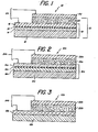
- Fig. 1 illustrates a useful Schottky barrier photovoltaic cell 10 prepared in the manner described above.
- a glass support 12 has deposited on it layers 14 and 16, selected as described above to form a low-resistance contact electrode 18.
- layer 14 is deposited as an oxide of a dopant
- layer 16 is deposited as a metal capable of reducing the dopant oxide.
- Interfacial region 19, represented by "x", Fig. 1, comprises the oxidation-reduction products of layers 14 and 16.
- a layer 20 of polycrystalline n-type CdTe is deposited to form the photosensitive element 21.
- the resulting photosensitive element provides a low-resistance contact to the CdTe layer of no greater than 20 ohm-cm 2. In the preferred embodiments, the resistance is less than 5 ohm-cm 2.
- a suitable barrier electrode layer 22 is deposited over layer 20.
- layer 22 is preferably at least semi-transparent.
- Wires or other suitable connectors 24 are soldered to each of the conductive layers 16 and 22, respectively, to connect the cell to a load or other electrical component. As with other Schottky barrier solar cells, such a cell is useful to generate electricity. Such uses are conventional and readily apparent to the skilled artisan.
- wires 24 are omitted and a plurality of the cells are fabricated into an integrated, series-connected array using, e.g., the procedure described in U.S. Patent No. 3,713,893.
- a large glass sheet 12 provides a common support for the cells in such an embodiment.
- layer 16 is deposited as two separate but contiguous layers, optionally of two different reducing metals.
- cell 10a comprises a support 12a, the two layers 14a and 16a, together with interfacial region 19a, comprising electrode 18a.
- a layer 20a of CdTe is disposed on layer 16a, and barrier electrode 22a completes the cell.
- Wires 24a allow connection of the cell to other electrical components.
- layer 16a of the reducing metal is in contact with support 12a, whereas layer 14a of the oxidized dopant contacts layer 20a.
- the electrode comprises a single admixture layer 19b, which after the oxidation-reduction reaction, comprises the elemental dopant, the oxidized metal, and optionally at least one of excess metal not oxidized and oxidized dopant not reduced.
- Layers 12b, 20b, 22b, and connectors 24b are as described for the other embodiments.
- Preferred photovoltaic cells produced in the manner described above have conversion efficiencies which exceed 6% when measured under sunlight or simulated sunlight of 75 mW/cm 2 intensity.
- a photosensitive element of the invention was prepared from which a photovoltaic cell was prepared.
- a layer of Ti about O.lum (1000A) thick was vacuum deposited on cleaned and degreased indium oxide-coated glass available under the trademark "Nesatron” glass from PPG Industries.
- n-CdTe about 50 ⁇ m thick was deposited over the Ti layer by the sublimation process described above using a vacuum of 2.66 Pa (2 X 10 -2 torr).
- the source of CdTe was an undoped, hot-pressed tablet, which was heated to 650°C by a radiation source during deposition.
- the temperature of the two-layer electrode during CdTe deposition was maintained at 330° to 410°C by a similar heat source, and the deposition continued for about 3.5 minutes.
- the resulting n-type CdTe film was heat-treated in air at 382°C for 3 minutes.
- the cell was completed by vacuum depositing a semi-transparent layer of Au which became the barrier electrode of the solar cell.
- the performance of the solar cell was determined by measuring the current-voltage (I-V) relationship under illumination falling on the Au electrode and transmitted in part through that electrode.
- the shape of the I-V curve thus obtained was such that no current saturation in the forward-voltage direction was detected, indicating that the contact is ohmic with a resistance of less than 20 ohm-cm 2 between the CdTe and the electrode.
- the cell Under an irradiance of 75 mW/cm 2 of simulated sunlight, the cell showed a conversion efficiency of 6.1 percent.
- a solar cell was prepared in a manner similar to that described in Example 1, except that the CdTe source additionally contained about 0.05 weight percent of CdI 2 ; the electrode temperature during CdTe deposition was approximately 335°C; the source temperature was 630°C; and the deposition time was 5 minutes.
- the resulting cell had a conversion efficiency of 7.1 percent when measured in the same manner as in Example 1.
- a cell was prepared using a glass support, a layer of dopant oxide as set forth in Table II, a layer of reducing metal as set forth in Table II, a layer of n-type CdTe and a gold barrier electrode about 100A thick, all in the format of the cell of Fig. 1.
- Dopant oxides listed as "Nesatron” were obtained by using Nesatron glass supports and those designated as In 2 0 3 were coated using a 133 x 10 -5 Pa (10 -5 torr) conventional vacuum evaporator (as were the other dopant oxides listed). The metal layers were coated using the same vacuum evaporator.
- the CdTe layer was about 25 um thick, coated as in the procedure of Example 1 except that the source was heated to a temperature of about 680°C, the electrode to be coated was at a temperature of about 450°C, and the pressure of the coater was about 8 Pa (6 X 10- 2 torr). CdTe coating times were about 90 sec.
- the electrical properties of the cell were determined using simulated AM2 illumination, that is, light of an intensity of 75 mW/cm 2.
- the total forward resistance R D of Table II was measured from the slope of the I-V curves so obtained, of which I sc and V oc are stated in the table (short-circuit current and open-circuit voltage, respectively). From this, R c , the contact resistance of the electrode to the CdTe layer, was estimated by subtracting the resistance of the Au barrier electrode, of the CdTe layer, and of the electrode, and then multiplying by the cell area (0.1 cm 2 ). Each of the subtracted resistances was estimated based upon measurements taken from a representative number of samples.
- the Au resistance is normally 20 to 45 ohms, the CdTe resistance about 25 ohms, and the electrode resistance about 20 ohms.
- the estimated error for the Rc values of Table II is + 200%. With this error range, even the examples with the highest measured Rc values do not exceed a contact resistance of about 20 ohm-cm2.
- Controls 3, 4 and 5 all involved the use of a "reducing" metal that is not capable of reducing In 2 O 3 , as is evident from the location of the oxide of that metal in Table I.
- the contact resistance for such controls was greater than 800 ohm-cm 2 (the maximum determinable value being 800 ohm-cm 2 ).
Landscapes
- Photovoltaic Devices (AREA)
- Physical Deposition Of Substances That Are Components Of Semiconductor Devices (AREA)
Applications Claiming Priority (2)
| Application Number | Priority Date | Filing Date | Title |
|---|---|---|---|
| US32322581A | 1981-11-20 | 1981-11-20 | |
| US323225 | 1981-11-20 |
Publications (1)
| Publication Number | Publication Date |
|---|---|
| EP0080342A2 true EP0080342A2 (de) | 1983-06-01 |
Family
ID=23258246
Family Applications (1)
| Application Number | Title | Priority Date | Filing Date |
|---|---|---|---|
| EP82306171A Withdrawn EP0080342A2 (de) | 1981-11-20 | 1982-11-19 | Lichtempfindliches Element, Verfahren zu seiner Herstellung, und photovoltaische Zelle, die dieses Element enthält |
Country Status (4)
| Country | Link |
|---|---|
| EP (1) | EP0080342A2 (de) |
| JP (1) | JPS5892282A (de) |
| AU (1) | AU9072982A (de) |
| CA (1) | CA1189173A (de) |
Cited By (4)
| Publication number | Priority date | Publication date | Assignee | Title |
|---|---|---|---|---|
| EP0118579A1 (de) * | 1981-09-08 | 1984-09-19 | Sohio Commercial Development Co. | Fotovoltäische Dünnschichtheterojunktionszellen und Verfahren zu ihrer Herstellung |
| US4568792A (en) * | 1984-02-02 | 1986-02-04 | Sri International | Photovoltaic cell including doped cadmium telluride, a dislocation preventing agent and improved ohmic contacts |
| US4697202A (en) * | 1984-02-02 | 1987-09-29 | Sri International | Integrated circuit having dislocation free substrate |
| US20220285569A1 (en) * | 2017-02-27 | 2022-09-08 | First Solar, Inc. | Thin film stacks for group v doping, photovoltaic devices including the same, and methods for forming photovoltaic devices with thin film stacks |
Families Citing this family (1)
| Publication number | Priority date | Publication date | Assignee | Title |
|---|---|---|---|---|
| JP2018039959A (ja) | 2016-09-09 | 2018-03-15 | タツタ電線株式会社 | 導電性接着剤組成物 |
-
1982
- 1982-07-08 CA CA000406855A patent/CA1189173A/en not_active Expired
- 1982-11-18 JP JP57202861A patent/JPS5892282A/ja active Pending
- 1982-11-19 EP EP82306171A patent/EP0080342A2/de not_active Withdrawn
- 1982-11-19 AU AU90729/82A patent/AU9072982A/en not_active Abandoned
Cited By (5)
| Publication number | Priority date | Publication date | Assignee | Title |
|---|---|---|---|---|
| EP0118579A1 (de) * | 1981-09-08 | 1984-09-19 | Sohio Commercial Development Co. | Fotovoltäische Dünnschichtheterojunktionszellen und Verfahren zu ihrer Herstellung |
| US4568792A (en) * | 1984-02-02 | 1986-02-04 | Sri International | Photovoltaic cell including doped cadmium telluride, a dislocation preventing agent and improved ohmic contacts |
| US4697202A (en) * | 1984-02-02 | 1987-09-29 | Sri International | Integrated circuit having dislocation free substrate |
| US20220285569A1 (en) * | 2017-02-27 | 2022-09-08 | First Solar, Inc. | Thin film stacks for group v doping, photovoltaic devices including the same, and methods for forming photovoltaic devices with thin film stacks |
| US12261231B2 (en) * | 2017-02-27 | 2025-03-25 | First Solar, Inc. | Thin film stacks for group V doping, photovoltaic devices including the same, and methods for forming photovoltaic devices with thin film stacks |
Also Published As
| Publication number | Publication date |
|---|---|
| JPS5892282A (ja) | 1983-06-01 |
| AU9072982A (en) | 1983-05-26 |
| CA1189173A (en) | 1985-06-18 |
Similar Documents
| Publication | Publication Date | Title |
|---|---|---|
| US4536607A (en) | Photovoltaic tandem cell | |
| EP0186351B1 (de) | Verfahren zur Herstellung eines Stromkollektorgitters und Werkstoffe dafür | |
| US4213798A (en) | Tellurium schottky barrier contact for amorphous silicon solar cells | |
| US4163677A (en) | Schottky barrier amorphous silicon solar cell with thin doped region adjacent metal Schottky barrier | |
| US4737197A (en) | Solar cell with metal paste contact | |
| AU647286B2 (en) | Improved solar cell and method of making same | |
| EP0274890B1 (de) | Dauerhafte ohmische Kontakte für p-leitende, Tellur enthaltende II-VI-Halbleiterschichten | |
| US4239553A (en) | Thin film photovoltaic cells having increased durability and operating life and method for making same | |
| US4758525A (en) | Method of making light-receiving diode | |
| KR19990063990A (ko) | 부분적으로 깊게 확산된 에미터가 있는 자가조정식(salde) 태양 전지 및 그 제조 방법 | |
| CN85107988A (zh) | 多结半导体器件 | |
| GB2044529A (en) | Amorphous silicon solar cells incorporating a thin insulating layer and a thin doped layer | |
| JPS6231835B2 (de) | ||
| JPH1056190A (ja) | 光起電力素子及びその製造方法 | |
| US4320248A (en) | Semiconductor photoelectric conversion device | |
| US4278704A (en) | Method for forming an electrical contact to a solar cell | |
| CN112133769A (zh) | 太阳能电池及其制造方法 | |
| JP3619681B2 (ja) | 太陽電池及びその製造方法 | |
| US4666569A (en) | Method of making multilayer ohmic contact to thin film p-type II-VI semiconductor | |
| GB2085657A (en) | Photovoltaic solar cells | |
| US4495375A (en) | MIS or SIS Solar cells | |
| EP0080342A2 (de) | Lichtempfindliches Element, Verfahren zu seiner Herstellung, und photovoltaische Zelle, die dieses Element enthält | |
| US20100307561A1 (en) | Doped metal contact | |
| CA1236224A (en) | Multilayer ohmic contact for p-type semiconductor and method for making same | |
| McCandless et al. | A treatment to allow contacting CdTe with different conductors [solar cells] |
Legal Events
| Date | Code | Title | Description |
|---|---|---|---|
| PUAI | Public reference made under article 153(3) epc to a published international application that has entered the european phase |
Free format text: ORIGINAL CODE: 0009012 |
|
| AK | Designated contracting states |
Designated state(s): DE FR GB NL |
|
| STAA | Information on the status of an ep patent application or granted ep patent |
Free format text: STATUS: THE APPLICATION IS DEEMED TO BE WITHDRAWN |
|
| 18D | Application deemed to be withdrawn |
Effective date: 19850531 |
|
| RIN1 | Information on inventor provided before grant (corrected) |
Inventor name: RAYCHAUDHURI, PRANAB KUMAR Inventor name: LIN, ALICE WEI-LUNG LEE |