EP0079098A1 - Amplifier with signal-dependent voltage supply source - Google Patents
Amplifier with signal-dependent voltage supply source Download PDFInfo
- Publication number
- EP0079098A1 EP0079098A1 EP82201345A EP82201345A EP0079098A1 EP 0079098 A1 EP0079098 A1 EP 0079098A1 EP 82201345 A EP82201345 A EP 82201345A EP 82201345 A EP82201345 A EP 82201345A EP 0079098 A1 EP0079098 A1 EP 0079098A1
- Authority
- EP
- European Patent Office
- Prior art keywords
- signal
- amplifier
- output
- feedback
- limiter
- Prior art date
- Legal status (The legal status is an assumption and is not a legal conclusion. Google has not performed a legal analysis and makes no representation as to the accuracy of the status listed.)
- Granted
Links
Images
Classifications
-
- H—ELECTRICITY
- H03—ELECTRONIC CIRCUITRY
- H03F—AMPLIFIERS
- H03F1/00—Details of amplifiers with only discharge tubes, only semiconductor devices or only unspecified devices as amplifying elements
- H03F1/02—Modifications of amplifiers to raise the efficiency, e.g. gliding Class A stages, use of an auxiliary oscillation
- H03F1/0205—Modifications of amplifiers to raise the efficiency, e.g. gliding Class A stages, use of an auxiliary oscillation in transistor amplifiers
- H03F1/0211—Modifications of amplifiers to raise the efficiency, e.g. gliding Class A stages, use of an auxiliary oscillation in transistor amplifiers with control of the supply voltage or current
- H03F1/0216—Continuous control
- H03F1/0222—Continuous control by using a signal derived from the input signal
- H03F1/0227—Continuous control by using a signal derived from the input signal using supply converters
Landscapes
- Engineering & Computer Science (AREA)
- Power Engineering (AREA)
- Amplifiers (AREA)
Abstract
Description
- The invention relates to a combination of an amplifier and a signal-dependent supply voltage source coupled thereto, the supply voltage of this source varying in accordance with the signal which is amplified by the amplifier.
- Such a combination is described in the Netherlands patent application 7604175 which has been laid open for public inspection. To vary the supply voltage, this combination uses pulse-width modulation, it being possible to take the modulating signal from the input or from the output of the amplifier. Such a signal-dependent power supply is rather complicated owing to the use of separate oscillators and modulators for the pulse-width modulation and, in addition, is rather sensitive to component tolerances and load variations, while the required stability imposes exacting requirements on the design.
- The invention has for its object to provide a combination of an amplifier and a signal-dependent supply voltage source whose supply voltage can, with a low sensitivity to tolerances and load variations, adequately follow the instantaneous value of the amplifier output voltage at a fixed difference therefrom.
- According to the invention, the combination of an amplifier and a signal-dependent supply voltage source is characterized in that a portion of the said signal is applied to an input of a comparator whose output signal controls a limiter, a portion of the limiter output signal being applied as a feedback signal to a second input of the comparator through a filter and a feedback network in series, in such a manner that a highrfrequency oscillation is produced in the feedback loop farmed by the comparator, the limiter, the filter and the feedback network,in which a signal-dependent modulation of the pulse width and/or the pulse density of the pulse-shaped output signal of the limiter occurs, a supply voltage for the output portion of the amplifier being derived from the output of the said filter.
- The invention will now be further described by way of example with reference to an embodiment shown in the accompanying drawing.
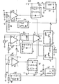
- The signal from a signal source 1 is applied to the non-inverting input of a control amplifier 2 whose supply terminals are connected to a
terminal 3 for a positive supply voltage and a terminal 4 for a negative supply voltage. The complementary outputs 2-1 and 2-2 of the control amplifier 2 control twocomplementary output stages 5 and 6 of a conventional construction. A load 7 is connected to the junction U of thestages 5 and 6. The other side of the load is at a reference potential (ground). - The
output stages 5 and 6 are located between the points P and Q and the load 7. Supply voltages of a positive and a negative polarity, respectively are applied to the points P and Q. Theoutput stages 5 and 6 together form a class-B amplifier and the junction U forms the output of the class-B amplifier. This output is fed back to the inverting input of control amplifier 2 through afeedback network 8. - The signal from signal source 1 is further applied to the non-inverting input of an
operational amplifier 9, whose output is fed back to its inverting input by way of theresistors 10 and 11. The output signal ofamplifier 9 is split into a positive portion bydiode 12 and into a negative portion bydiode 13. - The positive signal portion is applied to the non-inverting input of a
voltage comparator 16 by way of theresistors resistors 17 and 18 a small negative bias voltage is applied to the inverting input ofcomparator 16. The differential input voltage ofcomparator 16 is therefore larger than the positive signal portion by a small fixed amountV.
- The output signal of
comparator 16 is applied to the gate of a P-channel field effect switch 20 (MOSFET) by way of acontrol network 19. This field effect switch is connected between theterminal 3 and the point R, which is connected to ground through adiode 21. Theswitch 20 and thediode 21 together form a limiter circuit having the point R as its output, the point R being connected either to the positive supply voltage (switch 20 conducting;diode 21 cut-off) or to ground (switch 21 non-conducting;diode 21 conducting). - A portion of the output signal of the limiter 20-21 is applied to the inverting input of
comparator 16 via the series arrangement of a low-pass filter 22 and afeedback network 23. - An oscillation is produced in the feedback loop famed by the
components - The supply point P, mentioned above,of the class-B amplifier 5-6 is formed by the output of
filter 22. The output signal of thefilter 22 is the filtered version of the output signal of the limiter 20-21. This last-mentioned output signal is a pulse-width and/or pulse-density modulated pulse-shaped signal. The spectrum of this signal has a baseband portion which corresponds to the input signal, and further consists of double sidebands at either side of the oscillation frequency and the harmonics thereof. The low-pass filter 22 transmits the baseband signal and a portion of the higher frequency components. The degree to which these components are suppressed will depend on the ratio between the oscillation frequency of the loop and the resonant frequency offilter 22. A high oscillation frequency therefore has an advantageous effect. In one embodiment the oscillation frequency was 400 kHz and the resonant frequency offilter 22 was 40 kHz. - The voltage at the point P follows the positive portion of the output signal of
amplifier 9 at a fixed difference voltage VCE therefrom, which difference voltage is proportional to the bias voltage Δ V ofcomparator 16. - The negative portion of the output signal of
amplifier 9 is processed in the circuits shown in the lower portion of the Figure, which circuits correspond in a one-to-one relationship to the circuits shown in the upper portion of the Figure which process the positive signal portion. This correspondence is expressed in the Figures by using the same reference numerals but providing them with an accent notation. The only differences are that comparator 16' receives a small positive bias voltage at its inverting input, that the field effect transistor 20' is of the N-channel type and is connected to the terminal 4 and that the diode 21' is poled differently fromdiode 21. The result is that the voltage at point Q follows the negative portion of the output signal ofamplifier 9 at a fixed difference voltage VCE therefrom. - The signal at the output U of the class-B amplifier 5-6 is proportional to the output signal from signal source 1. By suitable choice of components it can be achieved that the voltage at point P follows the positive portion of the signal on output U at the fixed difference voltage VCE therefrom and that the voltage on point Q follows the negative portion of the signal of output U at the fixed difference voltage VCE therefrom. This choice results in the gain to points P and Q, respectively , from the signal source 1 being equal to the gain to output U from signal source 1. A possible way of realizing this is to make the attentuation cuased by the
resistors amplifier 9 and to make the transfer ratio of thefeedback network 8 for the signal frequencies equal to the transfer ratio of thefeedback network 23 and theresistor 18 for the signal frequencies. - During the positive signal portion at the output U the constant voltage VCE which is determined by the value ― 7 of the bias voltage of the
comparator 16 is present across the output stage 5; during the negative signal portion the constant voltage VCE is present across theoutput stage 6. ―V can be adjusted to be such that theoutput stage 5 or 6 carrying the output current for the load 7 receives sufficient voltage to linearly amplify the signal provided by amplifier 2. - The feedback factor of the feedback loops can be made large at the signal frequencies, as a result of which the supply voltages at the points P and Q can adequately follow the output signal of the amplifier to a large degree independently of the tolerenaces of the components and of any load variations.
- A certain time delay which becomes important at the higher signal frequencies occurs in the supply voltage circuits and is pre- dominatly caused by the
filters 22 and 22'. To prevent signal distortion from resulting in the signal path the same titre delay can be provided in the signal path. This can be realized by including two independent RC-filters . One of these PC-filters is thefilter 24, which is provided in the forward signal path between signal source 1 and amplifier 2. The other RC-filter is provided in the feedback path and is formed by thefeedback network 8, which for this purpose is in the form of a RC-filter. - The
feedback networks 23 and 23' are in the form of networks which are commonly referred to as phase lead networks. These networks shift the frequency at which a 1800 phase shift occurs in the feedback loops to a higher value, so that these loops will oscillate at a high to very high frequency. A high oscillation frequency relative to the highest signal frequency will result in significant suppression of the higher modulation products by thefilters 22 and 22', so that the supply voltages at the points P and Q will follow the signal on output U to the best possible extent.
Claims (4)
Applications Claiming Priority (2)
| Application Number | Priority Date | Filing Date | Title |
|---|---|---|---|
| NL8104914A NL8104914A (en) | 1981-10-30 | 1981-10-30 | AMPLIFIER WITH SIGNAL DEPENDENT SUPPLY SOURCE. |
| NL8104914 | 1981-10-30 |
Publications (2)
| Publication Number | Publication Date |
|---|---|
| EP0079098A1 true EP0079098A1 (en) | 1983-05-18 |
| EP0079098B1 EP0079098B1 (en) | 1986-01-15 |
Family
ID=19838290
Family Applications (1)
| Application Number | Title | Priority Date | Filing Date |
|---|---|---|---|
| EP82201345A Expired EP0079098B1 (en) | 1981-10-30 | 1982-10-28 | Amplifier with signal-dependent voltage supply source |
Country Status (5)
| Country | Link |
|---|---|
| US (1) | US4507619A (en) |
| EP (1) | EP0079098B1 (en) |
| JP (1) | JPS5884509A (en) |
| DE (1) | DE3268594D1 (en) |
| NL (1) | NL8104914A (en) |
Cited By (5)
| Publication number | Priority date | Publication date | Assignee | Title |
|---|---|---|---|---|
| GB2163311A (en) * | 1984-08-17 | 1986-02-19 | Philips Electronic Associated | Bipolar transistor rf power amplifier |
| EP0181613A2 (en) * | 1984-11-08 | 1986-05-21 | Spacelabs, Inc. | Improved power amplifier circuit |
| DE3744112A1 (en) * | 1987-12-01 | 1989-06-15 | Carl Spitzenberger | Amplifier arrangement |
| GB2227396A (en) * | 1988-12-29 | 1990-07-25 | Thomson Consumer Electronics | Dual power source deflection amplifier with signal-dependent higher power supply |
| DE19514450A1 (en) * | 1995-04-25 | 1996-10-31 | Thomson Brandt Gmbh | Power amplifier for LF signal |
Families Citing this family (30)
| Publication number | Priority date | Publication date | Assignee | Title |
|---|---|---|---|---|
| US5191606A (en) * | 1990-05-08 | 1993-03-02 | Industrial Technology Research Institute | Electrical telephone speech network |
| JP2669199B2 (en) * | 1991-06-20 | 1997-10-27 | ヤマハ株式会社 | Amplifier circuit and audio signal amplifier circuit |
| JP3132093B2 (en) * | 1991-09-25 | 2001-02-05 | ヤマハ株式会社 | Power supply circuit |
| US5450036A (en) * | 1993-02-23 | 1995-09-12 | Rohm Co., Ltd. | Power amplifier circuit for audio signal and audio device using the same |
| US5424684A (en) * | 1993-03-04 | 1995-06-13 | Rohm Co., Ltd. | Power amplifier circuit for audio signal and audio device using the same |
| KR0137105B1 (en) * | 1993-06-17 | 1998-04-29 | 모리시다 요이치 | Data-trasmission circuit, data-line driving circuit, amplifying circuit, semiconductor integrated circuit and semiconductor memory |
| US5396194A (en) * | 1993-11-19 | 1995-03-07 | Carver Corporation | Audio frequency power amplifiers |
| US5508658A (en) * | 1994-04-27 | 1996-04-16 | Rohm Co., Ltd. | Power amplifier circuit for audio signal and audio device using the same |
| US5606289A (en) * | 1994-06-22 | 1997-02-25 | Carver Corporation | Audio frequency power amplifiers with actively damped filter |
| US5543753A (en) * | 1994-06-22 | 1996-08-06 | Carver Corporation | Audio frequency power amplifiers with actively damped filter |
| US5554959A (en) * | 1994-10-25 | 1996-09-10 | Vac-Com, Inc. | Linear power amplifier with a pulse density modulated switching power supply |
| US5892404A (en) * | 1994-10-25 | 1999-04-06 | Vac-Com, Inc. | Linear power amplifier with a pulse density modulated switching power supply |
| US6130954A (en) * | 1996-01-02 | 2000-10-10 | Carver; Robert W. | High back-emf, high pressure subwoofer having small volume cabinet, low frequency cutoff and pressure resistant surround |
| US5777519A (en) * | 1996-07-18 | 1998-07-07 | Simopoulos; Anastasios V. | High efficiency power amplifier |
| EP0919107A1 (en) * | 1996-08-12 | 1999-06-02 | CARVER, Robert Weir | High back emf, high pressure subwoofer |
| US5898340A (en) * | 1996-11-20 | 1999-04-27 | Chatterjee; Manjirnath A. | High power efficiency audio amplifier with digital audio and volume inputs |
| US6104248A (en) * | 1998-10-23 | 2000-08-15 | Carver; Robert W. | Audio amplifier with tracking power supply utilizing inductive power converters |
| DE19909706A1 (en) * | 1999-03-05 | 2000-09-07 | Heidenhain Gmbh Dr Johannes | Method and circuit arrangement for mapping the mains voltage for regenerative supply devices |
| AU2001276206A1 (en) * | 2000-07-12 | 2002-01-21 | Indigo Manufacturing Inc. | Power amplifier with multiple power supplies |
| US6535399B2 (en) | 2001-08-14 | 2003-03-18 | Bose Corporation | Tracking power supply controlling |
| US7570931B2 (en) * | 2006-06-02 | 2009-08-04 | Crestcom, Inc. | RF transmitter with variably biased RF power amplifier and method therefor |
| GB2446843B (en) | 2006-06-30 | 2011-09-07 | Wolfson Microelectronics Plc | Amplifier circuit and methods of operation thereof |
| TWI477158B (en) | 2006-10-16 | 2015-03-11 | Thx Ltd | Loudspeaker line array configurations and related sound processing |
| JP2009135903A (en) * | 2007-10-16 | 2009-06-18 | Thx Ltd | Efficient power amplifier |
| US9425747B2 (en) * | 2008-03-03 | 2016-08-23 | Qualcomm Incorporated | System and method of reducing power consumption for audio playback |
| US8064851B2 (en) * | 2008-03-06 | 2011-11-22 | Crestcom, Inc. | RF transmitter with bias-signal-induced distortion compensation and method therefor |
| AU2010217899B2 (en) | 2009-02-25 | 2015-05-07 | Thx, Ltd. | Low dissipation amplifier |
| US8717211B2 (en) | 2010-11-30 | 2014-05-06 | Qualcomm Incorporated | Adaptive gain adjustment system |
| US9484860B2 (en) | 2013-03-12 | 2016-11-01 | Thx Ltd. | Tracking power supply with increased boost capability |
| US10473719B2 (en) * | 2017-10-12 | 2019-11-12 | Keysight Technologies, Inc. | System and method for separating and measuring two signals simultaneously present on a signal line |
Citations (4)
| Publication number | Priority date | Publication date | Assignee | Title |
|---|---|---|---|---|
| US3426266A (en) * | 1966-03-22 | 1969-02-04 | Collins Radio Co | Signal modulated self-regulated switching voltage regulatoramplifier |
| DE2407629A1 (en) * | 1974-02-18 | 1975-08-28 | Guenter Dipl Ing Kallina | High efficiency LF amplifier - switching amplifier designed as self-sustained oscillating control cct. |
| WO1980001023A1 (en) * | 1978-11-06 | 1980-05-15 | R Carver | High efficiency,light weight audio amplifier and power supply |
| FR2451671A1 (en) * | 1979-03-15 | 1980-10-10 | Tokyo Shibaura Electric Co | HIGH FREQUENCY SWITCHING CIRCUIT |
Family Cites Families (2)
| Publication number | Priority date | Publication date | Assignee | Title |
|---|---|---|---|---|
| JPS51121239A (en) * | 1975-04-17 | 1976-10-23 | Sony Corp | An amplification circuit |
| US4218660A (en) * | 1978-11-06 | 1980-08-19 | Carver R W | Audio amplifier and method of operating the same |
-
1981
- 1981-10-30 NL NL8104914A patent/NL8104914A/en not_active Application Discontinuation
-
1982
- 1982-10-25 US US06/436,539 patent/US4507619A/en not_active Expired - Fee Related
- 1982-10-28 EP EP82201345A patent/EP0079098B1/en not_active Expired
- 1982-10-28 DE DE8282201345T patent/DE3268594D1/en not_active Expired
- 1982-10-28 JP JP57189938A patent/JPS5884509A/en active Pending
Patent Citations (4)
| Publication number | Priority date | Publication date | Assignee | Title |
|---|---|---|---|---|
| US3426266A (en) * | 1966-03-22 | 1969-02-04 | Collins Radio Co | Signal modulated self-regulated switching voltage regulatoramplifier |
| DE2407629A1 (en) * | 1974-02-18 | 1975-08-28 | Guenter Dipl Ing Kallina | High efficiency LF amplifier - switching amplifier designed as self-sustained oscillating control cct. |
| WO1980001023A1 (en) * | 1978-11-06 | 1980-05-15 | R Carver | High efficiency,light weight audio amplifier and power supply |
| FR2451671A1 (en) * | 1979-03-15 | 1980-10-10 | Tokyo Shibaura Electric Co | HIGH FREQUENCY SWITCHING CIRCUIT |
Cited By (7)
| Publication number | Priority date | Publication date | Assignee | Title |
|---|---|---|---|---|
| GB2163311A (en) * | 1984-08-17 | 1986-02-19 | Philips Electronic Associated | Bipolar transistor rf power amplifier |
| EP0181613A2 (en) * | 1984-11-08 | 1986-05-21 | Spacelabs, Inc. | Improved power amplifier circuit |
| EP0181613A3 (en) * | 1984-11-08 | 1987-12-23 | Spacelabs, Inc. | Improved power amplifier circuit |
| DE3744112A1 (en) * | 1987-12-01 | 1989-06-15 | Carl Spitzenberger | Amplifier arrangement |
| GB2227396A (en) * | 1988-12-29 | 1990-07-25 | Thomson Consumer Electronics | Dual power source deflection amplifier with signal-dependent higher power supply |
| GB2227396B (en) * | 1988-12-29 | 1993-08-11 | Thomson Consumer Electronics | Dual power source output amplifier |
| DE19514450A1 (en) * | 1995-04-25 | 1996-10-31 | Thomson Brandt Gmbh | Power amplifier for LF signal |
Also Published As
| Publication number | Publication date |
|---|---|
| DE3268594D1 (en) | 1986-02-27 |
| EP0079098B1 (en) | 1986-01-15 |
| US4507619A (en) | 1985-03-26 |
| NL8104914A (en) | 1983-05-16 |
| JPS5884509A (en) | 1983-05-20 |
Similar Documents
| Publication | Publication Date | Title |
|---|---|---|
| EP0079098B1 (en) | Amplifier with signal-dependent voltage supply source | |
| JP4434557B2 (en) | Power amplifier circuit | |
| US4015213A (en) | Pulse width modulated signal amplifier | |
| US5672998A (en) | Class D amplifier and method | |
| US4524335A (en) | Pulse-width modulation circuit with carrier signal frequency control | |
| US4586000A (en) | Transformerless current balanced amplifier | |
| US4504793A (en) | Pulse-width modulation circuit | |
| CA1115360A (en) | Pwm signal power amplifier | |
| JPH053166B2 (en) | ||
| US4021745A (en) | Pulse width modulated signal amplifier | |
| US4437070A (en) | Amplifier arrangement whose overall gain is controllable by means of a control voltage | |
| CA1210089A (en) | Current source circuit arrangement | |
| US4435685A (en) | Amplifier arrangement | |
| KR900002089B1 (en) | Amplifier circuit | |
| JPH0336099Y2 (en) | ||
| EP4102717A1 (en) | Self-oscillating class d audio amplifier with voltage limiting circuit | |
| JPH0335846B2 (en) | ||
| JP2003152463A (en) | Separately-excited pulse width modulation d class power amplifier | |
| US4268796A (en) | Linear amplifier with distortion correction | |
| JPS63314904A (en) | Wide band amplifier circuit for multiplication detector | |
| JP2577946B2 (en) | Amplifier circuit | |
| JPS6340904Y2 (en) | ||
| JP2795964B2 (en) | Pulse width modulation type power amplifier | |
| RU2032981C1 (en) | Amplifier with pulse-duration modulation | |
| JPS58213568A (en) | Circuit for correcting video clamp |
Legal Events
| Date | Code | Title | Description |
|---|---|---|---|
| PUAI | Public reference made under article 153(3) epc to a published international application that has entered the european phase |
Free format text: ORIGINAL CODE: 0009012 |
|
| 17P | Request for examination filed |
Effective date: 19821028 |
|
| AK | Designated contracting states |
Designated state(s): DE FR GB |
|
| GRAA | (expected) grant |
Free format text: ORIGINAL CODE: 0009210 |
|
| AK | Designated contracting states |
Designated state(s): DE FR GB |
|
| REF | Corresponds to: |
Ref document number: 3268594 Country of ref document: DE Date of ref document: 19860227 |
|
| ET | Fr: translation filed | ||
| PLBE | No opposition filed within time limit |
Free format text: ORIGINAL CODE: 0009261 |
|
| STAA | Information on the status of an ep patent application or granted ep patent |
Free format text: STATUS: NO OPPOSITION FILED WITHIN TIME LIMIT |
|
| 26N | No opposition filed | ||
| PGFP | Annual fee paid to national office [announced via postgrant information from national office to epo] |
Ref country code: FR Payment date: 19891020 Year of fee payment: 8 |
|
| PGFP | Annual fee paid to national office [announced via postgrant information from national office to epo] |
Ref country code: GB Payment date: 19891031 Year of fee payment: 8 |
|
| PGFP | Annual fee paid to national office [announced via postgrant information from national office to epo] |
Ref country code: DE Payment date: 19891215 Year of fee payment: 8 |
|
| PG25 | Lapsed in a contracting state [announced via postgrant information from national office to epo] |
Ref country code: GB Effective date: 19901028 |
|
| GBPC | Gb: european patent ceased through non-payment of renewal fee | ||
| PG25 | Lapsed in a contracting state [announced via postgrant information from national office to epo] |
Ref country code: FR Effective date: 19910628 |
|
| PG25 | Lapsed in a contracting state [announced via postgrant information from national office to epo] |
Ref country code: DE Effective date: 19910702 |
|
| REG | Reference to a national code |
Ref country code: FR Ref legal event code: ST |