EP0078487A2 - Verfahren zur Herstellung eines dielektrischen Materials für elektrischen Isolator und erhaltenes dielektrisches Material - Google Patents
Verfahren zur Herstellung eines dielektrischen Materials für elektrischen Isolator und erhaltenes dielektrisches Material Download PDFInfo
- Publication number
- EP0078487A2 EP0078487A2 EP82109873A EP82109873A EP0078487A2 EP 0078487 A2 EP0078487 A2 EP 0078487A2 EP 82109873 A EP82109873 A EP 82109873A EP 82109873 A EP82109873 A EP 82109873A EP 0078487 A2 EP0078487 A2 EP 0078487A2
- Authority
- EP
- European Patent Office
- Prior art keywords
- dielectric
- glass
- manufacturing
- areas
- glass dielectric
- Prior art date
- Legal status (The legal status is an assumption and is not a legal conclusion. Google has not performed a legal analysis and makes no representation as to the accuracy of the status listed.)
- Granted
Links
Images
Classifications
-
- C—CHEMISTRY; METALLURGY
- C03—GLASS; MINERAL OR SLAG WOOL
- C03C—CHEMICAL COMPOSITION OF GLASSES, GLAZES OR VITREOUS ENAMELS; SURFACE TREATMENT OF GLASS; SURFACE TREATMENT OF FIBRES OR FILAMENTS MADE FROM GLASS, MINERALS OR SLAGS; JOINING GLASS TO GLASS OR OTHER MATERIALS
- C03C21/00—Treatment of glass, not in the form of fibres or filaments, by diffusing ions or metals in the surface
Definitions
- the present invention relates to a method of manufacturing a glass dielectric for an electrical insulator and a dielectric obtained by this method.
- Conventional glass dielectrics undergo a thermal toughening treatment such that they present on the surface significant compressive stresses and internally significant extension stresses. This results in a much improved mechanical resistance for the dielectric compared to that of annealed glass.
- the existence of internal stresses allows almost total fragmentation of the dielectric, which does not significantly or dangerously affect the residual mechanical resistance of the insulator, but reduces its line of flight at the distance in the air between the electrodes.
- the object of the present invention is to avoid this drawback and to produce an insulator dielectric capable of better withstanding impacts.
- the subject of the present invention is a process for manufacturing a glass dielectric for an electrical insulator, characterized in that one starts with an annealed glass dielectric and is subjected to chemical toughening at least in certain areas. of this dielectric; for this, a solution based on alkaline salts is applied to said zones, or to the complete dielectric, at ambient temperature, it is dried and then heated for a few hours at a temperature between 300 ° C. and 500 ° C. The treatment is carried out until the hardened zones have external compression constraints whose maximum values are greater than 1 00 Mega Pascal and internal extension constraints whose maximum values remain less than 10 Mega Pascal. These values must be obtained in particular at the critical places of the insulator likely to work mechanically.
- Said solution based on alkaline salts has a composition which can be of the following type: (percentages by weight):
- said solution corresponds to the following composition (percentages by weight)
- a preliminary treatment phase of the annealed glass can be provided to modify the surface composition of the glass so as to accelerate the ion exchanges during the chemical toughening.
- the invention also relates to a glass dielectric for an electrical insulator obtained by the above method; in the treated areas, the external compression stresses appear in a thickness of about 20 m M to 100 .mu.m.
- the treated areas are the areas most stressed mechanically, for example at the level of the insulator head. It may be simpler to process the entire dielectric.
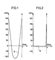
- Figures 1 and 2 show the distribution of stresses (in Mega Pascal) respectively in two samples A and B, sample A having undergone thermal quenching in accordance with the prior art, sample B having undergone chemical quenching according to l 'invention.
- the sample A which has undergone thermal hardening has compression stresses over a thickness of the order of 2 mm; the maximum value of these constraints is of the order of 250 MPa. It also presents significant internal constraints of extension, the maximum value of these constraints being of the order of 100 MPa.
- Sample B has been chemically quenched under the following conditions; the annealed sample was immersed in a solution at room temperature and having the following composition:
- This solution wets the glass very well and the dielectric is completely covered with a liquid film whose viscosity can be controlled.
- a drying operation is carried out followed by a heat treatment for 8 hours at a temperature of 500 ° C.
- curve B the distribution of extension and compression stresses in dielectric B.
- the maximum value of external compression stresses is around 200 MPa, while the maximum value of internal compression stresses is much less than 10 MPa.
- the thickness of the compression zone is of the order of 100 ⁇ m.
- the internal stresses of extension are low enough to avoid fragmentation of the sample in the event of a violent shock.
- the solution used for chemical quenching can be chosen from the following compositions (percentages given by weight):
- the starch can be replaced by an equivalent binder, for example of the emulsifiable adhesive type.
- Heating can last a few hours and the temperature can be between 300 ° C and 500 ° C.
- a dielectric B ′ according to the invention is thus obtained, the mechanical characteristics of which are recorded in table I below.
- the dielectric A ′ is a dielectric of the prior art thermally quenched under different conditions of temperature or hygrometry of the supply air.
- the glass initially contains potassium ions:
- the dielectric is soaked in a solution based on sodium nitrate, dried and heated to 450 ° C. To relax the constraints due to the ionic exchanges which have occurred, the part is then heated to a temperature higher than the glass transformation temperature. The chemical quenching is then carried out as defined above.
- the glass initially contains sodium ions:
- the dielectric is immersed in a solution based on lithium nitrate and sodium nitrate; it is dried and heated to around 350 ° C. To release the stresses due to the ionic exchanges which have taken place, the part is then heated to a temperature higher than the glass transformation temperature.
- Subsequent chemical quenching is done by soaking in a solution of a sodium salt, which allows an ion exchange between lithium and sodium. It can also be done by soaking in a solution of a sodium salt and a potassium salt which allows ionic exchanges between lithium and sodium on the one hand, and sodium and potassium on the other hand.
- the areas of the dielectric undergoing chemical quenching, during the treatment are subjected to an electric field in order to carry out an electromigration which effectively reinforces ionic exchanges.
- a piece of annealed glass is soaked in a bath of pure potassium nitrate at around 400 ° C. This part is subjected for one hour to an electric field of the order of 600V / cm.
- an electric field of the order of 600V / cm.
Landscapes
- Chemical & Material Sciences (AREA)
- Life Sciences & Earth Sciences (AREA)
- Engineering & Computer Science (AREA)
- Chemical Kinetics & Catalysis (AREA)
- General Chemical & Material Sciences (AREA)
- Geochemistry & Mineralogy (AREA)
- Materials Engineering (AREA)
- Organic Chemistry (AREA)
- Glass Compositions (AREA)
- Inorganic Insulating Materials (AREA)
- Surface Treatment Of Glass (AREA)
- Organic Insulating Materials (AREA)
Priority Applications (1)
| Application Number | Priority Date | Filing Date | Title |
|---|---|---|---|
| AT82109873T ATE16993T1 (de) | 1981-10-29 | 1982-10-26 | Verfahren zur herstellung eines dielektrischen materials fuer elektrischen isolator und erhaltenes dielektrisches material. |
Applications Claiming Priority (2)
| Application Number | Priority Date | Filing Date | Title |
|---|---|---|---|
| FR8120294 | 1981-10-29 | ||
| FR8120294A FR2515634A1 (fr) | 1981-10-29 | 1981-10-29 | Procede de fabrication d'un dielectrique en verre pour isolateur electrique et dielectrique en resultant |
Publications (3)
| Publication Number | Publication Date |
|---|---|
| EP0078487A2 true EP0078487A2 (de) | 1983-05-11 |
| EP0078487A3 EP0078487A3 (en) | 1983-07-20 |
| EP0078487B1 EP0078487B1 (de) | 1985-12-18 |
Family
ID=9263517
Family Applications (1)
| Application Number | Title | Priority Date | Filing Date |
|---|---|---|---|
| EP82109873A Expired EP0078487B1 (de) | 1981-10-29 | 1982-10-26 | Verfahren zur Herstellung eines dielektrischen Materials für elektrischen Isolator und erhaltenes dielektrisches Material |
Country Status (11)
| Country | Link |
|---|---|
| EP (1) | EP0078487B1 (de) |
| JP (1) | JPS58100309A (de) |
| AR (1) | AR240110A1 (de) |
| AT (1) | ATE16993T1 (de) |
| AU (1) | AU558928B2 (de) |
| BR (1) | BR8206274A (de) |
| CA (1) | CA1177652A (de) |
| DE (1) | DE3268055D1 (de) |
| FR (1) | FR2515634A1 (de) |
| NO (1) | NO155618C (de) |
| ZA (1) | ZA827891B (de) |
Cited By (1)
| Publication number | Priority date | Publication date | Assignee | Title |
|---|---|---|---|---|
| US4757162A (en) * | 1984-04-20 | 1988-07-12 | Ceraver | Rigid electrical insulator including a lightly tempered soda-lime glass dielectric |
Family Cites Families (4)
| Publication number | Priority date | Publication date | Assignee | Title |
|---|---|---|---|---|
| NL6500068A (de) * | 1965-01-06 | 1966-07-07 | ||
| DE1804839B1 (de) * | 1968-10-24 | 1969-12-04 | Jenaer Glaswerk Schott & Gen | Verfahren zur Verbesserung der mechanischen Festigkeit von Glas |
| US4042405A (en) * | 1976-03-18 | 1977-08-16 | American Optical Corporation | High strength ophthalmic lens |
| US4212919A (en) * | 1979-06-28 | 1980-07-15 | Corning Glass Works | Strengthened polychromatic glasses |
-
1981
- 1981-10-29 FR FR8120294A patent/FR2515634A1/fr active Granted
-
1982
- 1982-10-26 NO NO823548A patent/NO155618C/no unknown
- 1982-10-26 AT AT82109873T patent/ATE16993T1/de active
- 1982-10-26 EP EP82109873A patent/EP0078487B1/de not_active Expired
- 1982-10-26 DE DE8282109873T patent/DE3268055D1/de not_active Expired
- 1982-10-27 BR BR8206274A patent/BR8206274A/pt unknown
- 1982-10-27 AR AR291109A patent/AR240110A1/es active
- 1982-10-27 JP JP57188894A patent/JPS58100309A/ja active Granted
- 1982-10-28 CA CA000414421A patent/CA1177652A/fr not_active Expired
- 1982-10-28 ZA ZA827891A patent/ZA827891B/xx unknown
- 1982-10-28 AU AU89871/82A patent/AU558928B2/en not_active Ceased
Cited By (1)
| Publication number | Priority date | Publication date | Assignee | Title |
|---|---|---|---|---|
| US4757162A (en) * | 1984-04-20 | 1988-07-12 | Ceraver | Rigid electrical insulator including a lightly tempered soda-lime glass dielectric |
Also Published As
| Publication number | Publication date |
|---|---|
| JPS6313284B2 (de) | 1988-03-24 |
| AU558928B2 (en) | 1987-02-12 |
| JPS58100309A (ja) | 1983-06-15 |
| NO155618C (no) | 1987-04-29 |
| ZA827891B (en) | 1983-08-31 |
| BR8206274A (pt) | 1983-09-20 |
| NO155618B (no) | 1987-01-19 |
| EP0078487B1 (de) | 1985-12-18 |
| AR240110A1 (es) | 1990-01-31 |
| FR2515634A1 (fr) | 1983-05-06 |
| DE3268055D1 (en) | 1986-01-30 |
| FR2515634B1 (de) | 1984-10-26 |
| ATE16993T1 (de) | 1986-01-15 |
| CA1177652A (fr) | 1984-11-13 |
| AU8987182A (en) | 1983-05-05 |
| EP0078487A3 (en) | 1983-07-20 |
| NO823548L (no) | 1983-05-02 |
Similar Documents
| Publication | Publication Date | Title |
|---|---|---|
| EP0078488B1 (de) | Verfahren zur Herstellung eines in gehärtetem Glas dielektrischen materials für elektrischen Isolator und erhaltener Isolator | |
| KR102599962B1 (ko) | 산화물 단결정 박막을 구비한 복합 웨이퍼의 제조 방법 | |
| RU2009132524A (ru) | Способ изготовления термически обработанного изделия с покрытием с использованием покрытия из алмазоподобного углерода (dlc) и защитной пленки | |
| FR2640258A1 (fr) | Procede de fabrication de materiaux composites a renfort en fibres de carbure de silicium et a matrice ceramique | |
| FR2758338A1 (fr) | Procede de fabrication d'une piece superelastique en alliage de nickel et de titane | |
| CA2715174C (fr) | Procede de revetement d'une bande metallique et installation de mise en oeuvre du procede | |
| CN112410782A (zh) | 一种激光熔覆涂层材料的热处理方法 | |
| EP0078487A2 (de) | Verfahren zur Herstellung eines dielektrischen Materials für elektrischen Isolator und erhaltenes dielektrisches Material | |
| EP0784100A1 (de) | Eisen-Kobalt Legierung, Herstellungsverfahren für Band aus dieser Legierung, und die Erzeugnisse dieses Verfahren | |
| CN116043153B (zh) | 一种提高亚稳β钛合金双性能结构件强度和塑性的方法 | |
| FR2496706A1 (fr) | Procede de fabrication d'acier au silicium oriente | |
| CN111118367B (zh) | 一种难熔金属钼合金表面硅化物涂层的修复方法 | |
| CN114561527A (zh) | 一种316h钢锻件固溶处理晶粒度主动控制方法 | |
| WO1997032052A1 (fr) | Procede de traitement thermique d'un superalliage a base de nickel | |
| EP0235067B1 (de) | Verfahren zum Aufbringen von Schutzüberzügen auf metallurgischen Produkten | |
| JPS634627B2 (de) | ||
| FR2563843A1 (fr) | Procede de fabrication de plaques en alliage de titane | |
| JP3869172B2 (ja) | 脆性材の表面強靭化方法 | |
| FR2642438A1 (fr) | Procede pour former une couche d'oxyde de fer sur un objet en acier exempt de decarburation peripherique et application de ce procede | |
| FR3159176A1 (fr) | Procédé de fabrication de pièces dentées endurcies par nitruration, notamment de pièces pour turbomachine d’aéronef | |
| JPH0362770B2 (de) | ||
| FR2675816A1 (fr) | Procede pour la fabrication de toles d'aluminium. | |
| FR2587728A1 (fr) | Procede de traitement thermique d'une piece en alliage d'uranium | |
| CN119640202A (zh) | 一种铸造/喷射成形的金属件的表面净化处理方法 | |
| BE439840A (de) |
Legal Events
| Date | Code | Title | Description |
|---|---|---|---|
| PUAI | Public reference made under article 153(3) epc to a published international application that has entered the european phase |
Free format text: ORIGINAL CODE: 0009012 |
|
| AK | Designated contracting states |
Designated state(s): AT BE CH DE FR GB IT LI LU NL SE |
|
| PUAL | Search report despatched |
Free format text: ORIGINAL CODE: 0009013 |
|
| AK | Designated contracting states |
Designated state(s): AT BE CH DE FR GB IT LI LU NL SE |
|
| 17P | Request for examination filed |
Effective date: 19840112 |
|
| ITF | It: translation for a ep patent filed | ||
| GRAA | (expected) grant |
Free format text: ORIGINAL CODE: 0009210 |
|
| AK | Designated contracting states |
Designated state(s): AT BE CH DE FR GB IT LI LU NL SE |
|
| REF | Corresponds to: |
Ref document number: 16993 Country of ref document: AT Date of ref document: 19860115 Kind code of ref document: T |
|
| REF | Corresponds to: |
Ref document number: 3268055 Country of ref document: DE Date of ref document: 19860130 |
|
| PGFP | Annual fee paid to national office [announced via postgrant information from national office to epo] |
Ref country code: AT Payment date: 19861015 Year of fee payment: 5 |
|
| PLBE | No opposition filed within time limit |
Free format text: ORIGINAL CODE: 0009261 |
|
| STAA | Information on the status of an ep patent application or granted ep patent |
Free format text: STATUS: NO OPPOSITION FILED WITHIN TIME LIMIT |
|
| PG25 | Lapsed in a contracting state [announced via postgrant information from national office to epo] |
Ref country code: LU Free format text: LAPSE BECAUSE OF NON-PAYMENT OF DUE FEES Effective date: 19861031 |
|
| 26N | No opposition filed | ||
| PGFP | Annual fee paid to national office [announced via postgrant information from national office to epo] |
Ref country code: NL Payment date: 19871031 Year of fee payment: 6 |
|
| PG25 | Lapsed in a contracting state [announced via postgrant information from national office to epo] |
Ref country code: GB Effective date: 19881026 Ref country code: AT Effective date: 19881026 |
|
| PG25 | Lapsed in a contracting state [announced via postgrant information from national office to epo] |
Ref country code: SE Effective date: 19881027 |
|
| PG25 | Lapsed in a contracting state [announced via postgrant information from national office to epo] |
Ref country code: LI Effective date: 19881031 Ref country code: CH Effective date: 19881031 Ref country code: BE Effective date: 19881031 |
|
| BERE | Be: lapsed |
Owner name: CERAVER Effective date: 19881031 |
|
| PG25 | Lapsed in a contracting state [announced via postgrant information from national office to epo] |
Ref country code: NL Effective date: 19890501 |
|
| NLV4 | Nl: lapsed or anulled due to non-payment of the annual fee | ||
| PG25 | Lapsed in a contracting state [announced via postgrant information from national office to epo] |
Ref country code: FR Free format text: LAPSE BECAUSE OF NON-PAYMENT OF DUE FEES Effective date: 19890630 |
|
| REG | Reference to a national code |
Ref country code: CH Ref legal event code: PL |
|
| PG25 | Lapsed in a contracting state [announced via postgrant information from national office to epo] |
Ref country code: DE Effective date: 19890701 |
|
| GBPC | Gb: european patent ceased through non-payment of renewal fee | ||
| REG | Reference to a national code |
Ref country code: FR Ref legal event code: ST |
|
| EUG | Se: european patent has lapsed |
Ref document number: 82109873.8 Effective date: 19890619 |