EP0078034A1 - Data processing machine suitable for high-speed processing - Google Patents
Data processing machine suitable for high-speed processing Download PDFInfo
- Publication number
- EP0078034A1 EP0078034A1 EP82109783A EP82109783A EP0078034A1 EP 0078034 A1 EP0078034 A1 EP 0078034A1 EP 82109783 A EP82109783 A EP 82109783A EP 82109783 A EP82109783 A EP 82109783A EP 0078034 A1 EP0078034 A1 EP 0078034A1
- Authority
- EP
- European Patent Office
- Prior art keywords
- data
- memory
- bus
- output
- input
- Prior art date
- Legal status (The legal status is an assumption and is not a legal conclusion. Google has not performed a legal analysis and makes no representation as to the accuracy of the status listed.)
- Granted
Links
Images


Classifications
-
- G—PHYSICS
- G06—COMPUTING; CALCULATING OR COUNTING
- G06F—ELECTRIC DIGITAL DATA PROCESSING
- G06F9/00—Arrangements for program control, e.g. control units
- G06F9/06—Arrangements for program control, e.g. control units using stored programs, i.e. using an internal store of processing equipment to receive or retain programs
- G06F9/44—Arrangements for executing specific programs
- G06F9/448—Execution paradigms, e.g. implementations of programming paradigms
- G06F9/4494—Execution paradigms, e.g. implementations of programming paradigms data driven
Definitions
- the present invention relates to a data processing machine suitable for high-speed processing, and more particularly to a data processing machine fit for processing programs which require to be processed through repeated executions of a certain operation flow.
- a pipe line mode has been proposed as an architecture adaptable to high-speed processing required.
- This mode is based on parallel processing of data and is to control the respective operation flows (i.g., addition processing, subtraction processing, multiplication processing or division processing) for processing of programs in parallel.
- a processor system employing the pipe line mode is so structured that a plurality of arithmetic circuits each having a fixed single function, such as an adder or multiplier, are connected to each other in a ring form with a bus of the pipe line mode.
- This system is suitable for high-speed processing in that a plurality of operation flows can be executed in parallel.
- the operation system thus structured can produce an effect of the pipe line mode for the given processing, but has a defect that the performance is significantly reduced for other processings.
- Such reduction in the performance can be compensated to some degree by preparing the operation systems in accordance with the respective processings independently.
- the kinds of required arithmetic circuits are increased and the system structure is enlarged, thus resulting in a great increase of the cost.
- a computing time in each pipe line that is, a period of time necessary for data to be input to the pipe line and then output therefrom, is fixed and the individual pipe lines have different computing times from one another.
- Such prior microprocessor is operated in the control flow mode where the program counter is employed as an addresss specifying means to fetch instructions from the memory and the fetched instructions are decoded so as to process data. Consequently, such microprocessor is not suitable for high-speed processing because of the increased number of memory accesses.
- a data flow mode in which data is caused to flow through a bus, a certain arithmetic circuit takes out the data and the result is fed to the next arithmetic circuit through the bus, has the reduced number of memory accesses and hence is fit for high-speed processing.
- This mode has a feature such that predetermined arithmetic processings are carried out on the way of the bus, so that data is transferred while being treated sequentially and the final result is obtained at the end of the bus.
- the data flow mode has a disadvantage such that it is not useful the art of image processing including a number of those processings which do not require to be so much.
- An object of the invention is to provide a data processing machine which has a function to process a large amount of data at a high speed.
- Another object of the invention is to provide a data processing machine which can easily control designation and change of operations to be processed.
- Still another object of the invention is to provide a data processing machine which can execute the designated operation repeatedly.
- Still another object of the invention is to provide a novel microprocessor of modular type which can be easily coupled to a bus, ' and particularly which is coupled to a common bus to permit data transfer with respect to the general microcomputer.
- Still another object of the invention is to provide a processor in which an internal bus is coupled with an improved pipe line system, particularly in which a processing time in a pipe is variable.
- Still another object of the invention is to provide a processor in which executing sequence of operations is controlled with an improved data flow mode, and particularly which is suitable for prallel processing or composit processing.
- Still another object of the invention is to provide a novel processor in which the data flow mode and the pipe line mode are organically combined so as to obtain the respective advantages thereof in an additive manner.
- Still another object of the invention is to provide a data processing machine which is so structured that extensions can be realized with ease and the performance is improved in proportion to such extensions.
- Still another object of the invention is to provide a novel parallel-processing system in which a plurality of programmable microprocessors are coupled to each other via a common bus.
- Still another object of the invention is to provide a processor which can self-control input and output timing of information.
- Still another object of the invention is to provide a processor which can cotrol an amount of data to be input and an amount of data to be output.
- Still another object of the invention is to provide a data processing machine which is fit to execute such a program as including a number of processings that require changes to a relatively small degree.
- Still another object of the invention is to provide a novel microprocessor in which coupling between data to be treated and the associated instructions is separated on the program.
- Still another object of the invention is to provide a data processing machine which does not require to release an incomplete data on the way of the predetermined arithmetic processing sequence.
- Still another object of the invention is to provide a data processing machine which has a function not only to extinguish useless data but also to bypass irrelevant data.
- Still another object of the invention is to provide a data processing machine which has a copying function able to easily producing the same data at any desirous repeated number.
- Still another object of the invention is to provide a data processing machine which has a branching function to change processing in accordance with data or the reault of operation.
- Still another object of the invention is to provide a microprocessor which can perform loop operation therein.
- Still another object of the invention is to provide a microprocessor which has a function to detect the number of input data.
- Still another object of the invention is to provide a microprocessor which has a function to control a flow rate of data and is able to prevent an internal memory from falling into the overflow state.
- Still another object of the invention is to provide a data processing machine which has a function to execute processing and transfer of data in parallel through an internal ring and an operation ring and also which has a function to permit data transfer to and from other processors through an external ring.
- Still another object'of the invention is to provide an information processing machine which can control an outflow of information from the inside and an inflow of information from the outside in accordance with capacity of the memory.
- Still another object of the invention is to provide a data processing machine in a system which performs identification of the treated data using identified information, wherein data . is caused to flow in the same sequence with respect to the data having the same identified information.
- Still another object of the invention is to provide a microprocessor of modular type which can perform vector operation by using the pipe line mode with variable length.
- Still another object of the invention is to provide a data processing machine which can preset the desired operation sequence in a programmable manner without changing the kind of any arithmetic unit and arrangement thereof.
- a data processing machine comprises a first memory for storing destination addresses of data, a second memory for storing instructions, a third memory for storing the data, a fourth memory allowing the data from the third memory to wait for another, an arithmethic means for arithmetically processing the data output from the fourth memory, a bus for coupling these memories and the arithmetic means into a ring form, and an interface means coupled to the bus, the second memory being accessed with the destination addresses output from the first memory and the arithmetic means being controlled in accordance with the accessed instructions.
- the present invention is characterized in that the arithmetic means and the first to fourth memories are formed in a pipe line mode, the instructions input through the interface part are stored in the second memory, and arithmetic processing for data flowing through the ring-shaped bus is executed in the arithmetic means in accordance with instructions which are fetched from the second memory.
- the sequence of operations is controlled in the data flow mode within the ring.
- the sequence of operation can be programmably controlled in accordance with the arranged instructions in the second memory, so that various operations may be desirously executed without changing the kind of any arithmetic unit and arrangement thereof or increasing the number of units.
- the ring includes therein the third and fourth memories allowing data to wait for another, so that both data flows within the ring and out of the ring may be controlled effectively. Therefore, both processings indide and outside of the ring do not require to be subject to synchronous timing control based on common clock and they can be executed in an asynchronous relation therebetween, while data transfer between both the processings can be performed under precise timing control.
- the arithmetic part and the memory part are connected to each other through the ring-shaped bus, so that loop operation or repetitive operation may be executed at any desirous number without temporarily shelterring data out of the ring.
- loop operation or repetitive operation may be executed at any desirous number without temporarily shelterring data out of the ring.
- the data porcessing machine of this invention basically comprises a memory part capable of reading and writing, an arithmetic circuit part for selectively executing various operations, and an interface part for controlling data transfer to and from the outside.
- the memory part includes therein a transfer table memory (first memory) for storing destination addresses of data, a parameter table memory (second memory) being accessed with the addresses in the first memory and storing pnedetermined instructions, a data memory (third memory) for temprarily storing one half of input data for dyadic operation, and a queue memory (fourth memory) waiting a data to be processed by an arithmetic circuit.
- first memory for storing destination addresses of data
- second memory being accessed with the addresses in the first memory and storing pnedetermined instructions
- a data memory third memory for temprarily storing one half of input data for dyadic operation
- a queue memory fourth memory waiting a data to be processed by an arithmetic circuit.
- the arithmetic circuit part includes therein a processor unit for performing dyadic - operation or monadic operation, and a parameter table memory adapted to generate, extinguish and branch the data, to generate addresses for the data memory, to count the number of incoming data and to perform dyadic control.
- the present data processing machine is realized by such an architecture that the transfer table memory for storing destination addresses of data, the parameter table memory being accessed with the destination addresses and storing instructions, the data memory for temporarily stroing . one half of input data for dyadic operation,. the queue memory allowing the data from the data memory to wait for another and the processor unit performing dyadic or monadic operation for output from the queue memory and outputting the result to the transfer table memory are connected with a bus in a ring form, the bus is connected to a bus interface for controlling data transfer to and from an external bus, and the processor unit is operated in accordance with the instructions which have been desirously set in the parameter table memory at the time of initial setting.
- the foregoing architecture has such features as follows.
- the arithmetic circuit part with multi functions is concentrated in the processor unit.
- the transfer table memory, the parameter table memory, the data memory, the queue memory and the processor unit are coupled to each other with the ring-shaped bus.
- operation control in a data flow mode can be executed within the ring using the initially preset parameter table memory and data memory.
- bus interface for performing data transfer to and from external circuits-or external other machines.
- each block can be easily arranged into one module and the performance is improved just by coupling to a plurality of identical modules in series, corresponding to the number of coupled modules.
- it is enough only to wire an input terminal of one module with an output terminal of the other module.
- both the pipe line mode and data flow mode are combined so as to produce their merits in an additive manner, thus providing a high-speed processing processor adaptable widely for various purposes.
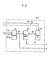
- FIG. 1 shows a block diagram of a data processing machine according to one embodiment of the invention.
- a bus interface (BI) 1, transfer table memory (TT) 2, parameter table memory (PT) 3, data memory (DM) 4, queue memory (QM) 5 and a processor unit (PU) 6 are arranged into one module.
- the transfer table memory 2, parameter table memery 3, data memory 4, queue memory 5 and the processor unit 6 are connected in due sequence with a bus of pipe line mode so as to form a ring shape.
- Input/output data transferred to and from external circuits includes module number setting data, template setting data, template reading data, data memory setting data, data memory reading data, resetting data, ineffective data, passing data, executing data, error status data, and processing data.
- the module number setting data comprises only the module number and is to set the module number into a module number register within the bus interface 1 when reset. After setting, the content of the module number register remains unchanged until a reset signal will become newly active.
- the content of the module number register is used to be compared with the module number of data taken into the processing module of the present invention after resetting.
- the template setting data comprises the module number, address for the transfer table memory 2, a data value written into the transfer table memory 2, address for the parameter table memory 3 and a data value written into the parameter table memory 3.
- the template setting data is to set template data into the transfer table memory 2 and the parameter table memory 3.
- the template data includes such data as representing the content and procedure of processing and is normally transferred into the processing module as shown in Fig. 1, that is, into the transfer table memory 2 and the parameter table memory 3, from a host processor of the outside at the starting of a required program processing.
- the template reading data comprises the module number, address for the transfer table memory 2 and address for the parameter table memory 3.
- the template reading data is to read the template data set in the transfer table memory 2 and the parameter table memory 3.
- the module number there is used the number of module which is intended to read the template data therefrom.
- the template reading data can be utilized to check the content of the template data in the event there occurs an error.
- the template reading data serves to output the read-out data value to the external circuit, but the module number at this time is replaced of the specified module number (e.g., 1) in order to discriminate it from other data.
- the data memory setting data comprises the module number and a data value, and is to write the data value into the data memory 4. Addresses used for writing the data value into the data memory 4 are generated from the parameter table memory 3 while being sequentially incremented one by one from 0.
- the data memory reading data comprises the module number and address for the data memory 4.
- the data memory reading data is to access the data memory 4 with the address for the data memory 4 included therein and to output the read-out data value to the external circuit.
- the resetting data comprises only the module number and is used to release the error state after there has occurred such state within the processing module of Fig. 1.
- the error state is resulted from an overflow error in the queue memory 5. If this error occurs, the data input to the bus interface 1 is not taken into the processing module and is extinguished.
- the resetting data is input to the bus interface 1, the error state is released and normal processing will be continued after that.
- the resetting data has another function to initialize the state within the processing module, that is, to clear counters and memories included therein. The resetting data disappears within the bus interface 1.
- the ineffective data comprises only the specified module number (e.g., 0). This data will disappear within the bus interface 1, even if it should be input. to the processing module shown in Fig. 1.
- the passing data represents such data as having therein the module number which does not coincide with the content of the module number register set at the time of resetting, and as not constituting the ineffective data as well as the module number setting data.
- the passing data directly passes through the bus interface 1 and is then output to the external circuit.
- the executing data comprises the module number, address for the transfer table memory 2, a cotrol bit, a code bit and a data value.
- the control bit will be set when the result of operation in the processor unit 6 coincides with the designated condition. In the case the control bit is set, address in the transfer table memory 2 is changed upon the designation of a branching instruction by the processor unit 6. Stated differently, in such case the data will be processed in a manner . different from the data where control bit is not set.
- the branching instruction is used to change a flow of processing in accordance with the operation result.
- the error status data comprises the module number and error status.
- the error status data has a function to inform the external circuit of the occurrence of error, when there occurs an overflow error in the queue memory 5 within the processing module.
- the module number included in the error status data corresponds to the read-out content of the module number register set within the module which has been subject to the error.
- the processing data comprises the module number, address for the transfer table memory 2, a control bit, a code bit and a data value.
- the processing data makes reference to the transfer table memory 2 and the parameter table memory 3.
- the processing data is added with address for the transfer table memory 2 and the module number obtained by referring to the transfer table memory 2 and the parameter table memory 3, and then output to the external circuit.
- the executing data comprises the module number, address for the transfer table memory 2, a control bit, a code bit and a data value.
- This data is taken into the ring-shaped bus of pipe line mode from the external circuit via the bus interface 1 and then sent to the transfer table memory 2.
- the data is allowed to be input from the external circuit into the processing module only on such conditions that the processor unit 6 is not under output operation, the number of data stored in the queue memory 5 is less than a certain value (e.g., 16 data), and the module number included in the input data coincides with the content of the module number register which has been taken therein at the time of resetting.
- the data input from the external circuit to the bus interface 1 is added with a use bit within the bus interface 1 and then sent to the transfer table memory 2.
- the transfer table memory 2 receives data from the bus interface 1 or the pro- cesssor unit 6.
- the data input to the transfer table memory 2 comprises a data value, address for the transfer table memory 2,a use flag and a template flag.
- the use flag is to indicate whether the data is effective or ineffective.
- the transfer table memory 2 checks both use flags of output data from the processor unit 6 and the bus interface 1, and then takes therein the data with its use flag assuming "1". In the case both use flags assume "1", the output data from the processor unit 6 is taken in with priority. The data in such a case where both use flags assume "0”, will turn to ineffective data. This ineffective data passes through the transfer table memory 2, parameter table memory 3 and the data memory 4, and then it disappears before reaching the queue memory 5.
- the transfer table memory 2 judges the input data as normal processing data, so that the transfer table memory 2 is accessed with the address for the transfer table memory 2 and then the read-out data is sent to the parameter table memory 3.
- the data is written into and read out from the transfer table memory 2 with the control bit.
- the data written into the transfer table memory 2 comprises information to discriminate processings before and after the reference to the transfer table memory 2, and information to discriminate paired components from each other when addresses used for newly referring to the transfer table memory 2, addresses used for referring to the parameter table memory 3 and the data sent to the parameter table memory 3 are operated as a pair, respectively, after data processing in the processor unit 6.
- the parameter table memory 3 is referred with the address for the parameter table memory 3, which is included in the data read out from the transfer table memory 2.
- the parameter table memory 3 mainly stores therein codes of instructions. Such codes include information to control data exchange where two data are operated as a pair, code information to designate the number of output data, the module number attached to the data taken out to the external circuit and the content of processing in the processor unit 6, and information for supervising the states such as reading or writing of the data memory 4, dyadic queue control of data or flow rate control thereof.
- Writing of data into the parameter table memory 3 is effected when the template flag is set, and the data is divided into permanent information which content remains unchanged during normal processing and temporary information which constitutes address information for the data memory 4.
- the parameter table memory 3 receives the use flag, template flag, control bit, instruction code and a data exchange signal from the transfer table memory 2, and it outputs a write enable signal to the data memory 4.
- the data memory 4 is used for storing a queue in which the data having reached in advance is allowed to temporarily wait until both data for dyadic operation (i.e., operation using two kinds of data as input) will be all present, a constant used for constant operation, a look up table, a transition table for processing the transition of state, and input/output data.
- the write enable signal for the data memory 4 is sent from the parameter table memory 3. With the instruction of dyadic operation being designated and both data being all present, input data from the parameter table memory 3 and read data from the data memory 4 are output to the queue memory 5 at the same time.
- the queue memory 5 comprises a data queue and a generator. queue.
- the data queue serves as.- a memory for temporarily holding data in the case the processor unit 6 outputs the plural number of data or receives data from the bus interface 1, because the processor unit 6 becomes busy and unable to input any more data at that time.
- the generator queue receives starting data for generating a numerical value, the number of generated data and control information from the data memory, and it outputs data to the processor unit 6 upon checking the information indicative of whether or not the data queue has a vacant space more than a predetermined value ( a half of capacity of the data queue in this embodiment).
- the processor unit 6 comprises arithmetic circuits which have various functions to permit arithmetic operation, logical operation, shift, comparison, bit inversion, priority encoding, branching, generation of numeric value, and copying.
- the bit inversion means such processing as providing an output data value which has an inverted bit position with respect to an input data value.
- priority encoding a value of each bit included in the input data value is sequentially checked from a bit with highest priority to a bit with lowest priority. As a result of this check, when there appears a bit which assumes "1" for the first, a position of the _bit is indicated in the form of binary integer and this is turned into the output data value.
- the branching performes such processing that upon checking the control bit, the address for the template memory 2 included in the input data is directly output as the address for the template memory 2 included in the output data with the control bit assuming "0", while address obtained by incrementing the address for the template memory 2 included in the input data is output as the address for the template memory 2 included in the output data with the control bit assuming "1".
- the generation of numeric value performs such processing as which checks a data value in the input data, the number of generatios and an increment value, then adds the increment value to the data value in the input data corresponding to the number of generations, and then issues the output data corresponding to the number of generations.
- This function is used in the case of including repetitive processing or including a need to generate addresses for the memory. On this occasion, the address for the transfer table memory 2 in the output data remains unchanged and the address for the transfer table memory 2 in the input data is directly output.
- the copying performs such processing that a data value in the input data and the number of copyings are checked and the data value in the input data is directly copied into the output data corresponding to the number of co p yings.
- the address for the transfer table memory 2 included in the output data assumes a value which is obtained by incrementing the address for the transfer table memory 2 in the input data one by one in sequence of outputs.
- the number of input data to the processor unit 6 is one or two, while the number of output data can be designated to have a range of 1 to 16. Processing where the number of input data is one is called as monadic operation (or monomial operation), and processing where the number of input data is two is called as dyadic operation. In the case of monadic operation, it is not required to make waiting because the number of input data is one , while in the case of dyadic operation (or binomial operation), the data having reached in advance is stored in a dyadic queue within the data memory to make waiting because it is impossible to execute operation until both data will be completely present.
- monadic operation or monomial operation
- dyadic operation or binomial operation
- the delayed data when it has reached, it is sent to the processor unit 6 through the queue memory 5 together with the former data read out from the dyadic queue within the data memory.
- the dyadic operation will be subject to execution control in a data flow mode.
- a busy flag is set while being output so as to inhibit the data to be input from the queue memory 5.
- Fig. 2 is a block diagram showing the bus interface 1 in Fig. 1 in more detail.
- the reference numeral 11 denotes an input latch
- 12 denotes an input buffer memory
- 13 denotes an output buffer memory
- 14 denotes an output latch
- 15 denotes a bus controller
- 16 denotes a reset signal
- 17 denotes a clock signal
- 18 denotes an input demand signal
- 19 denotes an input permission signal
- 20 denotes an output demand signal
- 21 denotes an output permission signal
- 22 denotes an input bus
- 23 denotes an output bus.
- data on the input bus 22 is taken into a module number register within the input latch of the bus interface included in the processing module.
- the reset signal 16 is not active, the data is input and output in a normal manner.
- the input demand signal 18 being active, data on the input bus 22 is taken into the input latch 11.
- the module number included in the data latched by the input latch 11 coincides with the content of the module number register, the data is taken into the input buffer memory 12, while in the case of not meeting such coincidence, the data is passed to the external circuit through the output latch 14.
- the data having the specified module number (e.g., the module number 0) is treated as ineffective data.
- the latched data is assumed as ineffective data and then will disappear within the input latch 11.
- a use flag is added to the data which is transferred from the input latch 11 to the input buffer memory 12.
- the input demand signal 18 When inputting data from the external circuit into the processing module, the input demand signal 18 is made active and the input data is fed to the input bus 22. Within the processing module, the input demand signal 18 is sampled synchronously with the clock signal 17. In the presence of an input demand and with input being permissible, the sampled data is latched into the input latch 11 irrespective of the module number on the input data. Then, the input permission signal 19 is made active and the external circuit is informed of that the data on the input bus 22 has been taken in.
- the input buffer memory 12 is to receive data from the input latch 11 and to temporarily store it therein.
- the output buffer memory 13 is to receive data from the data queue within the queue memory 5 of Fig. 5 and to store data which is output to the external circuit through the output latch 14.
- priority is given to the data output to directly pass through the processing module, so that the processed output data serves to latch the data from the data queue in the absence of such passing data.
- the data is added with the module number allocated to ineffective data and then output to the external circuit as ineffective data.
- the designated operation will be executed with blocks coupled into a ring shape.
- the ring it is possible to perform not only pipe line processing but also repetitive operation such as copy operation.
- data is not required to be taken out of the ring during its processing, thus permitting high-speed processing.
- write enable parameter table memory and transfer table memory so that the kind of operations and the sequence thereof may be selected desirously. It becomes possible, therefore, to effect the pipe line processing with variable length. The same operation can be executed for different data without changing the memory content, thus permitting to execute advanced processings such as vector operation with ease and at a high speed.
- the queue memory which has an important role as an output timing control mechanism for the data read out to an external bus through the bus interface.
- the result of operation processed within the ring is stored into the queue memory in sequence. Accordingly, if the operation result will be continued to be formed in the state where the queue memory issues no output, there may occour an overflow.
- the queue memory allowing the data to wait for another is subject to an overflow of data, this overflow has to be detected thereby to perform error processing.
- the overflow error is a fatal error, so that even if the execution is started once again, the system will be soon fallen into the overflow error.
- a processing speed is increased by executing the processing within the module independently of, that is, asynchronously with that on the outside, so that it is not appropriate to monitor the overflow error in the queue memory from the outside. Therefore, the overflow is required to be prevented within the module before it happens.
- a hardwar circuit should be used to realize this.
- an amount of data stored in the queue memory is monitored at all times and read-out from the queue memory is controlled in accordance with the amount of data, thereby to prevent an overflow in the queue memory.
- the queue memory is added with a queue memory control circuit with which an amount of data stored in the queue memory is monitored at all times and an overflow is prevented before it happens, by temporarily forbidding read-out from the queue memory or changing the priority sequence of read-out from the queue memory, in the event the sum of the monitored amount of data and an amount of data genetated at one time exceeds capacity of the queue memory.
- the present invention also provides a queue memory comprising a data que memory allowing the data with no possiblity of generation to wait for another, a generator queue memory allowing the data with a possibility of generation to wait for another, a counter for counting an amount of data stored in the data queue memory, a register for storing an upper limit value in the amount of data to be stored in the data queue memory, and a comparator for judging whether the value of the counter exceeds the value of the register or not, read-out from the data queue memory and the generator queue memory being selectively controlled in accordance with the compared result from the comparator.
- the queue memory includes therein the data queue (DQ), the generator queue (GQ) and an output queue (OQ), and further is composed of a. counter for counting an amount of data stored in the queue memory, a comparator for judging whether the value of the counter exceeds a difference of ((capacity of the queue memory) - (the maximum value of data genetated at one time by the generator)) or not, and a control circuit for controlling read-out from the queue memory.
- Fig. 3 shows a block diagram of one embodiment of the queue memory.
- the queue memory shown in Fig. 3 can be replaced of the queue memory 5 used in the data processing machine of Fig. 1.
- the data queue serves as a memory for temporarily holding input data in the case the processor 6 outputs the plural number of data or receives data from the bus interface 1, because the processor unit 6 becomes busy and unable to input any more data at that time.
- the generator- queue serves as a memory adapted to receive starting data for generating a numerical value, the number of generated data and control information from the data memory, and it issues output to the processor unit 6 upon checking the information indicative of whether or not the data queue has a vacant space more than a predetermined value (a half of capacity of the data queue in this embodiment).
- the processor unit 6 performs not only processing where the number of input data is one (i.e., monadic operation) but also processing where the number of input data is two (i.e., dyadic operation).
- monadic (monomial) operation it is not required to make waiting because the number of input data is one, while in the case of dyadic operation, the data having reached in advance is stored in a dyadic queue within the data memory 4 to make waiting because it is impossibe to execute operation until both data will be completely present.
- the delayed data when it has reached after waiting, it is transferred to the processor unit 6 through the queue memory 5 together with the former data read out from the dyadic queue within the data memory, and thereafter the d yadic (binomial) operation will be started.
- a busy flag is set during a period of output thereby to forbid the data to be input from the queue memory 5.
- the data output from the queue memory 5 includes therein;
- the number of data is reduced in the cases of (1), (2) and (3), while the number of data is increased in the cases of (4), (5) and (6).
- the number of data is greatly increased in the cases of (4) and (5), so that it is effective to control the data in such cases for the purpose of preventing an overflow in the queue memory.
- the reference numeral 101 denotes a data queue memory
- 102 denotes a queue memory control circuit
- 103 denotes a generator queue memory
- 104 denotes a multiplexer.
- the numeral 111 denotes data written into the data queue memory 101, that is, which data is output from the data memory 4 shown in Fig. 1 and input to the data queue memory 101.
- the numeral 112 denotes data which is read out from the data queue memory and then input to the multiplexer 104.
- the numeral 114 denotes a control signal and addresses for the data queue memory 101.
- the numeral 115 denotes data written into the generator queue memory 103, that is, which data is output from the data memory 4 shown in Fig. 1 and input to the generator queue memory 103.
- the numeral 116 denotes a control signal and addresses for the generator queue memory 103.
- the numeral 117 denotes data which is read out from the generator queue memory 103 and input to the multiplexer 104.
- the numeral 118 denotes output data from the multi- p lexer 104, which data is output to the multiprocessor 6 shown in Fig. 1.
- the numeral 113 denotes an input selection signal for the multiplexer 104. In response to this signal either one of the output data 112 from the data queue memory 101 and the output data 117 from the generator queue memory 103 is selected and then output from the multiplexer 104 as output data 118.
- the data stored in the data queue memory 101 corresponds to data which is output to the processor unit 6 in Fig. 1 through the multiplexer 104. This data is not accompanied with generation of data, so that its number will not be increased.
- the data stored in the generator queue memory 103 corresponds to data which is output to the processor unit 6 in Fig. 1 through the multiplexer 104, and this data is accompanied with generation of data. Therefore, the number of data is increased in the processor unit 6 shown in Fig. 1, so that the processor unit 6 falls into the busy state during such a period and becomes unable to input any more data.
- An amount of data stored in the data queue memory 101 is limited by capacity of the data queue memory.
- the data queue memory 101 is brought into the state of overflow so that the result of data processing may not be obtained correctly. Since an overflow is one of fatal errors, any further execution of program becomes impossible and hence processing is interrupted at once when fallen into that state. Thus, it is required to provide a means for preventing the interruption of processing before it happens.
- read-out from the generator queue memory 103 should be forbidden in the case there is a possibility that the data queue memory 101 may come into an overflow.
- read-out from the generator queue memory 103 is given with higher priority than that of read-out from the data queue memory 101 so as to prevent reduction of the performance which is resulted from the absence of data in the data queue memory 101.
- Fig. 4 shows a detailed block diagram of the queue memory control circuit 102 shown in Fig. 3.
- the circuit 102 includes therein a counter 211, a comparator 212 and a register 213.
- the reference numeral 221 denotes data written into the register 213 and 222 denotes a write pulse fed to the register 213.
- An upper limit setting value for preventing an overflow in the data queue memory 101 is preset into the register 213 by the write pulse 222. Through the subsequent processing, the preset value remains unchanged.
- a reset signal 223 is to clear the counter 211 prior to processing.
- the numeral 224 denotes a clock signal for the counter 211.
- a value of the counter 211 is incremented by one when the clock signal 224 is input to the counter 211.
- a value of the counter 211 is decremented by one when the clock signal 224 is input to the counter 211.
- the value of the counter 211 indicates the number of data stored in the data queue memory 101 shown in Fig. 3 at present. Thus, upon write into the data queue memory 101, the value is incremented by one, while upon read-out from the da ⁇ a queue memory 101, the value is decremented by one.
- the reference numeral 226 denotes data read-out from the counter 751 and sent to the comparator 752 and the queue memory 645 in Fig. 6.
- the numeral 767 denotes data read out from the register 213, that is, the upper limit setting value as mentioned above.
- the comparator 212 makes comparison between the output data 114 from the counter 211 and the output data 226 from the register 213. As a result of the comparison, if the output data 114 from the counter 211 is larger, there issues a queue memory switching signal, that is, a signal 227 for forbidding read-out from the generator queue memory 103. Upon this signal 227, read-out from the generator queue memory 103 is forbidden and priority is given to read-out from the data queue memory 101.
- the data processing machine of this invention is characterized in that for the purpose of preventing an overflow in the queue memory allowing data to wait for another, there is included the queue control circuit which monitors an amount of data stored in the queue memory and which controls read-out from the queue memory to avoid occurrence of the overflow. More specifically, data accompanied with generation of data and another data accompanied with no generation of data are separately stored in the different que memories, and read-out from the generator oueue memory for storing the data accompanied with generation of data is controlled in accordance with an amount of data present in the data queue memory for storing the data accompanied with no generation of data.
- This control is performed so as to .forbid read-out from the generator queue memory when the sum of the maximum amount of data generated at one time and the amount of data stored in the data queue memory exceeds capacity of the data queue memory.
- the above shows an exemplified structure in which an overflow in the queue memory is prevented beforehand by controlling read-out from the queue memory in accordance with an amount of data stored therein (particularly an amount of data sent to the processor unit). According to this structure, it becomes possible to execute processing with no interruption, because the queue memory will never fall into the overflow state even if the processor unit becomes busy.
- Fig. 5 shows a block diagram of thus arranged system.
- three modules 511, 512 and 513 are serially connected through pipe line buses 521, 522, 523 and 524 in the unidirection.
- Control signals 531, 532, 533 and 534 fed in the direction opposite to a flow of the data are input to and output from the modules, respectively.
- Each adjacent processor modules can be directly connected to each other without a need of any attached external circuit, so that an increase in the number of processor modules can easily realize the improved performance corresponding to that number.
- multistage connection Such a structure in which a plurality of processor modules are directly connected in series, will be now referred to as multistage connection.
- a problem encountered in the multistage connection is how to allocate the required processings to the respective processor modules. In other words, it is demanded to find an allocation method which ensures the higher performance, without producing no fear of overflow in the data queue memory within each processor module.
- the processor system including the multistage connection with the respective processor modules having a large variation in their processing times, data is jammed in the processor module having a longer p recessing time, so that there occurs an overflow in the queue memory.
- an amount of data stored in the queue memory is monitored at all times and data input from the external circuit is temporarily forbidden when the monitored data amount exceeds an upper limit preset with respect to capacity of the queue memory, thus restraining the generation of data in the previous processor module.
- the remaining processor modules can be controlled to operate.' at a speed which is suitable for the processor module hving the largest processing amount and the lowest processing speed among all of the connected modules.
- the present invention is able to provide a processor system which can perform control of the multistage connection.
- the system accoding to this embodiment icludes therein a counter for counting an amount of data stored in the queue memory, a comparator for judging whether or not a value of the counter exceeds an upper limit, that is, an value of (capacity of the queue memory) - (the number of latches constituting the piep line), and a control circuit adapted to forbid input from the external circuit in accordance with output from the comparator.
- Fig. 6 shows a block diagram of one module.
- This module icludes therein a bus interface (BI) 641, a transfer table memory (TT) 642, a parameter table memory (PT) 643, a data memory (DM) 644, a queue memory (QM) 645, a processor unit (PU) 646 and an input data control circuit (IC) 647.
- TT 642, PT 643, DM 644, QM 645 and PU 646 are connected into a ring shape with a pipe line bus in the sequence as illustrated in the drawing.
- Destination address for data is stored in the TT 642.
- the PT 643 is accessed with the destination address output from the TT 642 and stores therein instructions transferred from a host processor in the initialized state.
- the DM 644 serves as a memory for temporarily storing one half of input data for dyadic operation.
- the QM 645 serves as a queue memory allowing to make waiting of data from the DM 644.
- the PU 646 is a processor unit which has a function to perform dyadic operation (i.e., operation for two kinds of input data) or monadic operation (i.e., operation for one kind of input data) with respect to output from the QM 645.
- the BI 641 is an interface circuit for controlling the input/output transfer of data between the pipe line bus and the external bus.
- the PT 643 has such additional functions as to permit generation, extinction and branching of data, counting of incoming data, dyadic control, and address generation for the DM 644.
- the input data control cirucit 647 controls the BI 641 upon checking the state of the QM 645.
- p ut/output treated in the BI 641 includes module number setting data, template setting data, template reading data, data memory setting data, data memory setting data, data memory reading data, resetting data, ineffective data, passing data, executing data, error status data, and processing data.
- the module number setting data comprises only the module number and is to set the module number into a module number register within the bus interface 641 when reset. After once being set upon resetting, the content of the module number register remains unchanged until a reset signal will become newly active. The content of the module number register is used to be compared with the module number of data taken into the processing module after resetting.
- the template setting data comprises the module number, address for the transfer table memory 642, a data value written into the transfer table memory 642, address for the parameter table memory 643 and a data value written into the parameter table memory 643.
- the template setting data is to set template data into the transfer table memory 642 and the parameter table memory 643.
- the template data represents the content and procedure of processing and is normally transferred into the internal processing module, that is, into the transfer table memory 642 and the parameter table memory 643, from a host processor on the outside at the starting of serial processing.
- the template reading data comprises the module number, address for the transfer table memory 642 and address for the parameter table memory 643.
- the template reading data is to read the template data set in the transfer table memory 642 and the parameter table memory 643.
- the module number for the data there there is used the number of module which is intended to read the template data therefrom.
- the template reading data can be utilized to check the content of the template data in the event there occurs an error.
- the template reading data serves to output the read-out data value to the external circuit, but the module number at this time is replaced of the specified module number (e.g., 1) in order to discriminate it from other data.
- the data memory setting data comprises the module number and a data value, and is to write the data value into the data memory 644. Addresses used for writing the data value into the data memory 644 are generated from the parameter table memory 643 while being sequentially incremented one by one from 0.
- the data memory reading data comprises the module number and address for the data memory 644. The data memory reading data is to access the data memory 644 with the address for the data memory 644 included therein and to output the read-out data value to the external circuit.
- the resetting data comprises only the module number and is used to release the error state after there has occurred such state within the processing module.
- the error state is resulted from an overflow error in the queue memory 645. If this error occurs, the data input to the bus interface 641 is not taken into the processing module and is extinguished. But in the case the resetting data is input to the bus interface 641, the error state is released and normal processing will be continued after that.
- the resetting data has another function to initialize the state within the processing module, that is, to clear counters and memories included therein. The resetting data disappears within the bus interface 641.
- the ineffective data comprises only the specified module number (e.g., 0). This data will disappear within the bus interface 641, even if it should be input to the processing module.
- the passing data represents such data as having therein the module number which does not coincide with the content of the module number register set at the time of resetting, and as not constituting the ineffective data as well as the module number setting data.
- the passing data input from the external data directly passes through the bus interface 641 and is then output to the external circuit. This means the bypassing of data.
- the executing data comprises the module number, address for the transfer table memory 642, a control bit, a code bit and a data value.
- the control bit is set when the result of operation in the processor unit 646 coincides with the designated condition.
- address in the transfer table memory 642 is changed upon the designation of a branching instruction by the processor unit 646. Stated differently, in such case the data will be processed in a manner different-from the data where the control bit is not set. With the branching instruction not being designated, no change of processing will occur so that the control bit and the branching instruction are normally used as a pair.
- the branching instruction is used to change a flow of processing in accordance with the operation result.
- the error status data comprises the module number and error status.
- the error status data has a function to inform the external circuit of the occurrence of error, when there occurs an overflow error in the queue memory 645 within the processing module.
- the module number included in the error status data corresponds to the read-out content of the module number register set within the module which has been subject to the error.
- the processing data comprises the module number, address for the transfer table memory 642, a control bit, a code bit and a data value.
- the processing data makes reference to the transfer table memory 642 and the parameter table memory 643.
- the processing data is added with address for the transfer table memory 642 and the module number obtained by referring to the transfer table memory 642 and the parameter table memory 643, and then output to the external circuit.
- the executing data comprises the module number, address for the transfer table memory 642, a control bit, a code bit and a data value.
- This data is taken into the ring-shaped bus of pipe line mode from the external circuit via the bus interface 641 and then sent to the transfer table memory 642.
- the data is allowed to be input from the external circuit into the processing module only on such conditions that the processor unit 6 is not under output operation, the number of data stored in the queue memory 645 is less than a certain value (e.g., 16 data), and the module number included in the input data coincides with the content of the module number register which has been taken therein at the time of resetting.
- the data input from the external circuit to the bus interface 641 is added with a use bit within bus interface 641 and then sent to the transfer table memory 642.
- the transfer table memory 642 receives data from the bus interface 641 or the processor unit 646.
- the data input to the transfer table memory 642 comprises a data value, address for the transfer table memory 642, use flag and a template flag.
- the use flag is to indicate whether the data is effective or ineffective.
- the transfer table memory 642 checks both use flags of output data from the processor unit 646 and the bus interface 641, and then takes therein the data with its use flag assuming "1". In the case both use flags assume "1", the output data from the processor unit 646 is taken in with priority. The data in such a case where both use flags assume "0", will turn to ineffective data. This ineffective data passes through the transfer table memory 642, parameter table memory 643 and the data memory 644, and then it disappears before reaching the queue memory 645.
- the transfer table memory 642 judges the input data as normal processing data, so that the transfer table memory 642 is accessed with the address for the transfer table memory 642 and then the read-out data is sent to the parameter table memory 643. With the use flag assuming "1" and the template flag assuming "1”, the data is written into and read out from the transfer table memory 642 with the control-bit.
- the data written into the transfer table memory 642 comprises information to discriminate processings before and after the reference to the transfer table memory 642, and information to discriminate paired components from each other when addresses used for newly referring to the transfer table memory 642, addresses used for referring to the parameter table memory 643 and the data sent to the parameter table memory 643 are oprated as a pair, respectively, after data processing in the processor unit 646.
- the parameter table memory 643 is referred with the address for the parameter table memory 643, which is included in the data read out from the transfer table memory 642.
- the parameter table memory 643 mainly stores therein codes of instructions. Such codes include information to control data exchange where two data-are operated as a pair, code information to designate the number of output data, the module number attached to the data taken out to the external circuit and the content of processing in the processor unit 646, and information for supervising the states such as reading/writing of the data memory 644, dyadic queue control of data or flow rate control thereof.
- Writing of data into the parameter table memory 643 is effected when the template flag is set. This data is divided into permanent information which content remains unchanged during normal processing and temporary information which constitutes address information for the data memory 644.
- the parameter table memory 643 receives the use flag, template flag, control bit, instruction code and a data exchange signal from the transfer table memory 642, and it outputs a write enable signal to the data memory 644.
- the data memory 644 is used for storing a queue in which the data having reached in advance is allowed to temporarily wait until both data for dyadic operation (i.e., operating using two kinds of data as input) will be all present, a constant used for constant operation, a look up table, a transition table for processing the transition of state, and input/output data,
- the write enable signal for the data memory 644 is sent from the parameter table memory 643. With the instruction of dyadic operation being designated and both data being all present, input data from the parameter table memory 643 and read data from the data memory 644 are output to the queue memory 645 at the same time.
- the queue memory 645 comprises a data queue and a generator queue.
- the data queue serves as a memory for temporarily holding data in the case the processor unit 646 outputs the plural number of data or receives data from the bus interface 641, because the processor unit 646 becomes busy and unable to input any more data at that time.
- the generator queue receives starting data for generating a numerical value, the number of generated data and control information from the data memory, and it outputs data to the processor unit 646 upon checking the information indicative of whether or not the data queue has a vacant space more than a predetermined value (a half of capacity of the data queue in this embodiment).
- the processor unit 646 comprises arithmetic circuits which have various functions to permit arithmetic operation, logical operation, shift, comparison, bit inversion, priority encoding, branching, generation of numeric value, and copying.
- the bit inversion means such processing as providing an output data value which has an inverted bit position with respect to an input data 7 alue.
- a value of each bit included in the input data value is sequentially checked from a bit with highest priority to a bit with lowest priority. As a result of this check, when there appears a bit which assumes "1" for the first, a posi- tion of the bit is indicated in the form of binary integer and this is turned into the output data value.
- the branching performes such processing that upon checking the control bit, the address for the template memory 642 included in the input data is directly output as the address for the template memory 642 included in the output data with the control bit assuming "0", while address obtained by incrementing the address for the template memory 642 included in the input data is output as the address for the template memory 642 included in the output data with the control bit assuming "1".
- the generation of numeric value performs such processing as which checks a data value in the input data, the number of generations and an increment value, then adds the increment value to the data value in the input data corresponding to the number of generations, and then issues the output data corresponding to the number of generations.
- This function is used in the case of including repetitive processing or including a need to generate addresses for the memory. On this occasion, the address for the transfer table memory 642 in the output data remains unchanged and the address for the transfer table memory 642 in the input data is directly output.
- the copying performs such processing that a data value in the input data and the number of copyings are checked and the data value in the input data is directly copied into the output data corresponding to the number of copyings.
- the address for the transfer table memory 642 included in the output data assumes a value which is obatined by incrementing the address for the transfer table memory 642 in the input data one by one in sequence of outputs.
- the number of input data to the processor unit 646 is one or two, while the number of output data can be designated to have a range of 1 to 16. Processing where the number of input data is one is called as monadic operation, and processing where the number of input data is two is called as dyadic operation. In the case of monadic operation, it is not required to make waiting because the number of input data is one, while in the case of dyadic operation, the data having reached in advance is stored in a dyadic queue within the data memory 644 to make waiting because it is impossible to execute processing until both data will be completely present.
- the delayed data when it has reached, it is sent to the processor unit 646 through the queue memory 645 together with the former data read out from the dyadic queue within the data memory. Whereupon, the operation will be started. In other words, the dyadic operation will be subject to execution control in a..data flow mode.
- a busy flag is set while being output so as to inhibit the data to be input from the queue memory 645.
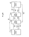
- Fig. 7 shows a block diagram showing one embodiment of the input data control circuit 647 shown in Fig. 6.
- This newly proposed circuit 647 includes therein a counter 751, a comparator 752 and a register 753.
- the reference numeral 761 denotes data written into the register 753, and 762 denotes a write pulse fed to the register 753.
- An upper limit setting value for preventing an overflow in the queue memory 645 shown in Fig. 6 is preset into the register 753 by the write pulse 762. Through the subsequent processing, the preset value remains unchanged.
- the reference numeral 763 denotes a reset signal, which is to clear the counter 751 prior to processing.
- the numeral 764 denotes a clock signal for the counter 751.
- a value of the counter 751 is incremented by one when the clock signal 764 is input to the counter 751. Meanwhile, with the up/down switching signal 765 assuming the down-state, a value of the counter 751 is decremented by one when the clock signal 764 is input to the counter 751.
- the value of the counter 751 indicates the number of data stored in the queue memory 645 shown in Fig.6 at present. Thus, upon write into the queue memory 645, the value is incremented by one, while upon read-out from the queue memory 645, the value is decremented by one.
- the reference numeral 766 denotes data read-out from the counter 751 and sent to the comparator 752 and the que memory 645 in Fig. 6.
- the numeral 767 denotes data read-out from the register 753, that is, the upper limit setting value as mentioned above.
- the comparator 752 makes comparison between the output data 766 from the counter 751 and the output data 767 from the register 753. As a result of the comparison, if the output data 766 from the counter 751 is larger, there issues a data input inhibition signal 768 which is output to the bus interface 641 shown in 6.
- This data input inhibition signal 768 is used as an input control signal in the bus interface 641, so that data input is forbidden while the data input inhibition signal 768 is active, that is, while the number of data stored in the queue memory 645 esceeds the aforesaid upper limit. As the data input inhibition signal 768 becomes inactive, data input will be started once again.
- the reason why a difference between capacity of the queue memory 645 and the number of latches constituting the pipe line is adopted as the upper limit value is as follows.
- the data in the queue memory 645 includes data to be output to the external circuit through the bus interface 641. At this time, if the bus in the external circuit is in the busy state, the data is unable to be output. But even such occasion, the latches constituting the pipe line continue operation thereof, so that data in amount corresponding to the number of latches is caused to flow into the queue memory 645 even with data input from the external circuit being inhibited, thus producing a possibility of overflow. Therefore, the upper limit value is determined to avoid such possibility.
- the data processing system is characterized in that for the purpose of preventing an overflow in the queue memory allowing data to wait for another, there is included the input data control circuit which monitors an amount of data stored in the queue memory and which inhibits input of data temporarily to avoid occurrence of the overflow.
- This control is performed so as to forbid input of data when the sum of the maximum amount of data generated at one time and the amount of data stored in the queue memory exceeds capacity of the queue memory.
- the number of data stored in the queue memory becomes less than the value of (capacity of the queue memory) - (data amount generated at one time)
- data input is released from is inhibited state and then started once again.
- Figs. 1 to 6 The data processing machine of modular type as shown in Figs. 1 to 6 is programmable and easy in bus connection, so that it is also fit for a composite processing system. In addition, since transfer of instructions to each module (that is, setting of the initial state) can be performed with ease, a general microcomputer is able to be used as a host processor.
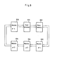
- Fig. 8 shows a block diagram of the system and there will be now described the structure and operation thereof.
- Fig. 8 is a block diagram showing an embodiment in which a plurality of modules are connected through a ring-shaped bus under pipe line control.
- a host processor 831 a main memory 832 and four modules (#1 to #4) 833 to 836 are coupled into a ring shape with the unidirectional bus.
- the respective modules #1 to #4 have the structure as illustrated in Fig. 1 or 6, and they serve as auxiliary processing machines for the host processor 831.
- the module number is loaded into a module number register within each module. Among data flowing through the ring-shaped bus, only the data which coincides with the loaded module number is taken into that module, while other data are controlled to pass through that module.
- initial setting data is sent from the host processor 831 to the respective modules 833 to 836.
- the initial setting data is to first set such data as instructions or control information necessary for processing into the parameter table memory 3, the data memory 4 and tne transfer table memory 2.
- the data to be set in the parameter table memory 3 and the transfer table memory 2 is referred to as a template.
- the subsequent processing will be performed in accordance with this template.
- Fig. 8 again.
- data such as image information has been input into the main memory 832 previously. This data is read out from the main memory 832 and subject to the desired processing in the respective modules 833 to 836, and then the result is written into the main memory 832.
- the respective modules 833 to 836 are connected through the bus under pipe line control.
- Each module has a composite processing function and is able to set the template therein, so that various processing functions different from one another may be set in the modules, respectively.
- most efficent processing is obtained and a processing speed is increased up to the maximum value.
- the structure as mentioned above has a feature that a high-speed in the pipe line made and parallel execution control in the data flow mode are effectively combined, and hence can realize high-speed processing with ease just by connecting a plurality of identical modules in series.
- the foregoing system is featured in permitting selection of functions in the arithmetic part with a composite function in response to the desired processing, and then makes it possible to reduce a vacancy in the arithmetic part for the connection using the ring-shaped bus.
- the performance can be significantly improved. It is enough to prepare one kind of module and this is preferable for a tendency toward LSI.
- the module structure can be arranged so as to fit for a flow of data and hence the number of collisions of data on the bus is reduced, thus making system design very easy.
- each of the processor modules is to execute predetermined serial arithmetic processing with use of the bus therein independently. So there is a possibility that the modules may have their processing times different from one another. On this occasion, when plural modules with their processing times having a great difference therebetween are connected through a common bus to constitute the system, this produces the module in which an input and output amount of data are different from each other.
- the queue memory serves as a memory to assuredly ensure P . that such difference in the input and output amounts is self-controlled in that module and there occurs no adverse influence upon other modules.
- capacity of the queue itself is fixed based on the hardware, it is unable to control a data flow exceeding the fixed capacity.
- the proposed data flow rate control circuit attention is directed to one of elements included in a set of data as a unit, for example zi and vi, so as to prevent an inflow of data exceeding capacity af the respective information processing machines in such a manner that an absolute value of the difference between the number of zi's sent from the information processing machine A to B and the number of vi's sent from the information processing machine B to A is monitored from time to time, and then this value is controlled not to exceed a given constant.
- the three data xi, yi and zi are given with-different discriminators such as '0', '1' and '2', respectively, while the two data ui and vi are similarly given with different discriminators such as '0' and '1'.
- Fig. 9 shows a block diagram of the. proposed data flow rate control circuit and a pair of information processing machines.
- data is required to be sent from an information processing machine #1 to another information processing machine #2 and a queue memory 900 with an FIFO function has therein a data storing area.
- the information processing machine #1 With a data receive enable signal being output on a signal line 902, the information processing machine #1 outputs iata to a data line 901, the data comprising a data discriminator and a data value.
- the queue memory 900 holds thus output data temporarily,
- the data discriminator is used to access a table memory 910 through a data line 904.
- a discriminator for new data having been stored in the table memory 910 is read out to a data line 906, while an increase monitor bit is read out to a signal line 914.
- a data value fed to a data line 905 and the discriminator for new data fed to the data line 906 are input to the information processing machine #2 through a data line 907 together.
- data input from the information processing machine #2 through a data line 911 is directly fed to the information processing machine #1 through a data line 918.
- the data discriminator is used to access an memory 920 through a data line 912 and then the accessed data is output to a signal line 913 as a decrease monitor bit.
- a counter 930 is incremented by one when the increase.
- monitor bit is output to the signal line 914, and is decremented by one when the decrease monitor bit is output to the signal line 913.
- An absolute value of the counter 930 is output to a data line 905 and then compared with output from a register 950 by a comparator 940. When the value on the data line 915 is less than the value on a data line 916, a value of '1' is output to a signal line 917. If the information processing machine #2 is under the state able to receive data, a value of '1' is output to a signal line 908. At the same time, with a value of '1' being output to the signal line 917, an output signal line 909 of a logical product circuit 960 assumes '1'.
- the queue memory 900 continues to read only when '1' is output to the signal line 909. In this embodiment, an output part corresponds to the queue memory 900, while an output control part corresponds to a block 300 shown by a broken line.
- Fig. 10 is a block diagram showing another embodiment.
- This embodiment represents the case that data transfer is mutually controlled between a pair of two information processing machines.
- a flow rate control circuit 20-1 When there exists data to be given from an information processing machine #11 to the other information processing machine #10 and a flow rate control circuit 20-1 outputs the data receiving enable state to a data line 70-1, data comprising a data discriminator and a data value is output from the information processing machine #11 to a data line 50-2.
- the dara discriminator has a function to discriminate data individually and the information processing machine #10 will be subject different processing for each discriminator.
- the data input from the data line 50-2 is added in a flow rate control circuit 20-2 with an increase monitor bit in accordance with the discriminator and then input ro the flow rate control circuit 20-1 through a data line 30-1 to be stored therein temporarily.
- the flow rate control circuits 20-1 and 20-2 are composed of circuits of the same construction.
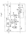
- Fig. 11 is an exemplified block diagram showing the flow rate control circuit 20-1 in more detail.
- a table memory 204 is accessed with the discriminator input through the data line 50-1, while a decrease and increase monitor bit are output to signal lines 256 and 255, respectively.
- the input data on the data line 50-1 and the increase monitor bit on the signal line 255 are fed to the flow rate control circuit 20-2 in Fig. 10 through the data line 30-2.
- a counter 202 is decremented by one.
- the increase monitor bit and data input to the data line 30-1 from the flow rate control circuit 20-2 in Fig. 10 are temporarily stored in a queue memory 200.
- the queue memory 200 When the queue memory 200 is under the state capable of storing data therein, the data receiving enable state is output to the information processing machine #11 in Fig. 10 through the signal line 70-1.
- the increase monitor bit read out from the queue memory 200 is fed through a signal line 251 to increment the counter 202 by one, while the data therefrom is fed to the information processing machine #10 in Fig. 10 through the data line 40-1.
- An absolute value of the counter 202 is output to a data line 257 and then compared with the value of the register 201 by a comparator 203. If the value on the data line 258 is larger than the value on the data line 257, a value of '1' is output to a data line 259. In the opposite relation, a value of '0' is output thereto.
- a signal indicating the data input enable state is input from the information processing machine #10 in Fig. 10 through the signal line 60-1, then logical product of the value on the signal line 259 and the value on the signal line 60-1 is obtained by a logical product circuit 205, and then the result is output to a signal line 260.
- the register 202 and the table memory 204 may be replaced of a constant generator and a read-only memory, respectively.
- a data flow rate control circuit used for transferring data between at least two information processing machines A and B each treating data consisted of a discriminator and a data value, which circuit comprises; an output part holding data input from the information processing machine A and including FIFO adapted to output the held data to the information processing machine B; and an output control part for counting the number of data fed from the information processing machine B to the information processing machine A while checking the data discriminator therein, counting the number of data output from the output part to the information processing machine B while checking the data discriminator therein, and then controlling output from the output part so as to maintain a difference between both the counted values within a p re- determined value.
- sequence and time for processing of data can be changed in a programmable manner, thus permitting pipe line processing with variable length and high-speed data processing.
- the machine includes therein a bus structure of closed loop, whereby multiple loop operation and copying operation can be executed with ease. There are included functions to extinguish ineffective data or bypass useless data, so that the program may be processed with an operation flow having no loss. Since the machine includes therein a means to branch a data flow in accordance with data or the result of operation, it becomes possible with a simple circuit loop to execute such processing as corresponding conditional branch processing or so in the program.
- both an amount of incoming data and an amount of outgoing data are able to be monitored and controlled, whereby data can be transferred to and from external processors or memories with neither loss nor error.
- the machine can be used to arrange a system of three-ring structure comprising an outer ring, an inner ring and an operation ring, so that it is highly suitable for multiprocessing.
- a novel microprocessor by which the treated data and the associtated instructions are controlled to be separated from each other or coupled together in a programmable manner as required, thus providing a great effect in the art of data processing where a large number of data has to be treated.
Abstract
Description
- The present invention relates to a data processing machine suitable for high-speed processing, and more particularly to a data processing machine fit for processing programs which require to be processed through repeated executions of a certain operation flow.
- There has been heretofore adopted a control flow mode in microprocessors as well known. A basic process of this node is such that a necessary instruction is fetched by accessing to a memory, the fetched instruction is decoded to read out data and execute the processing specified by the instruction, and the result is stored in the memory. Such process is sequentially repeated so as to process a set of program. In order to apply the processor of this kind to the art (e.g., image processing or voice processing) which requires high-speed processing, there has been developed in the past such an attempt as improving an operating speed of semiconductor devices used for the processor or increasing the number of bits treated in the processor at the same time. In the present situation, however, the former is limited due to difficulties in the semiconductor manufacturing technology and the latter leads to an increase in size of the device and system and has a limit from the view point of economy.
- Under the background as mentioned above, a pipe line mode has been proposed as an architecture adaptable to high-speed processing required. This mode is based on parallel processing of data and is to control the respective operation flows (i.g., addition processing, subtraction processing, multiplication processing or division processing) for processing of programs in parallel. A processor system employing the pipe line mode is so structured that a plurality of arithmetic circuits each having a fixed single function, such as an adder or multiplier, are connected to each other in a ring form with a bus of the pipe line mode. This system is suitable for high-speed processing in that a plurality of operation flows can be executed in parallel. It is required, however, to select the kind of arithmetic circuits to be used and determine the sequence of the selected arithmetic circuits optimum for the given processing. Therefore, the operation system thus structured can produce an effect of the pipe line mode for the given processing, but has a defect that the performance is significantly reduced for other processings. Such reduction in the performance can be compensated to some degree by preparing the operation systems in accordance with the respective processings independently. But the kinds of required arithmetic circuits are increased and the system structure is enlarged, thus resulting in a great increase of the cost. Furthermore, a computing time in each pipe line, that is, a period of time necessary for data to be input to the pipe line and then output therefrom, is fixed and the individual pipe lines have different computing times from one another. As a result, in the case a plurality of processors of the pipe line mode are used to constitute the so-called multiprocessor, timing control of data transfer between the processors becomes very complicated. In addition, according to the conventional processor of the pipe line mode, it is difficult to cause processing to be looped within a pipe. Stated differently, processing can not be executed repeatedly within a single pipe line, so that such processing has required intricate software control and a prolonged processing time.
- Meanwhile, in the art requiring high-speed processing (e.g., image processing adapted to process images from satellites or of X-ray photograghs by a man-machine system), a large amount of data up to about 6 millions piccellsfor each image has to be processed in a short period of time. For instance, to process one image for 3 seconds, the image has to be processed at a speed of 500 ns per 1 piccell. It is required, therefore, that the processor itself has a function to permit high-speed processing and that data transfer between the processor and the memory can be performed at a high speed. Particularly, the latter is a major problem for the conventional microprocessor in which the memory is accessed by using a program counter. As mentioned above, such prior microprocessor is operated in the control flow mode where the program counter is employed as an adress specifying means to fetch instructions from the memory and the fetched instructions are decoded so as to process data. Consequently, such microprocessor is not suitable for high-speed processing because of the increased number of memory accesses.
- To the contrary, a data flow mode in which data is caused to flow through a bus, a certain arithmetic circuit takes out the data and the result is fed to the next arithmetic circuit through the bus, has the reduced number of memory accesses and hence is fit for high-speed processing. This mode has a feature such that predetermined arithmetic processings are carried out on the way of the bus, so that data is transferred while being treated sequentially and the final result is obtained at the end of the bus. In the data flow node, however, it is difficult to control a flow of data and make coupling with the prior microprocessor. Therefore, an effect meeting expectations can not be obtained in repetitive operations, parallel processing or composite processing using a common bus. In other words, the data flow mode has a disadvantage such that it is not useful the art of image processing including a number of those processings which do not require to be so much.
- An object of the invention is to provide a data processing machine which has a function to process a large amount of data at a high speed.
- Another object of the invention is to provide a data processing machine which can easily control designation and change of operations to be processed.
- Still another object of the invention is to provide a data processing machine which can execute the designated operation repeatedly.
- Still another object of the invention is to provide a novel microprocessor of modular type which can be easily coupled to a bus, ' and particularly which is coupled to a common bus to permit data transfer with respect to the general microcomputer.
- Still another object of the invention is to provide a processor in which an internal bus is coupled with an improved pipe line system, particularly in which a processing time in a pipe is variable.
- Still another object of the invention is to provide a processor in which executing sequence of operations is controlled with an improved data flow mode, and particularly which is suitable for prallel processing or composit processing.
- Still another object of the invention is to provide a novel processor in which the data flow mode and the pipe line mode are organically combined so as to obtain the respective advantages thereof in an additive manner.
- Still another object of the invention is to provide a data processing machine which is so structured that extensions can be realized with ease and the performance is improved in proportion to such extensions.
- Still another object of the invention is to provide a novel parallel-processing system in which a plurality of programmable microprocessors are coupled to each other via a common bus.
- Still another object of the invention is to provide a processor which can self-control input and output timing of information.
- Still another object of the invention is to provide a processor which can cotrol an amount of data to be input and an amount of data to be output.
- Still another object of the invention is to provide a data processing machine which is fit to execute such a program as including a number of processings that require changes to a relatively small degree.
- Still another object of the invention is to provide a novel microprocessor in which coupling between data to be treated and the associated instructions is separated on the program.
- Still another object of the invention is to provide a data processing machine which does not require to release an incomplete data on the way of the predetermined arithmetic processing sequence.
- Still another object of the invention is to provide a data processing machine which has a function not only to extinguish useless data but also to bypass irrelevant data.
- Still another object of the invention is to provide a data processing machine which has a copying function able to easily producing the same data at any desirous repeated number.
- Still another object of the invention is to provide a data processing machine which has a branching function to change processing in accordance with data or the reault of operation.
- . Still another object of the invention is to provide a microprocessor which can perform loop operation therein.
- Still another object of the invention is to provide a microprocessor which has a function to detect the number of input data.
- Still another object of the invention is to provide a microprocessor which has a function to control a flow rate of data and is able to prevent an internal memory from falling into the overflow state.
- Still another object of the invention is to provide a data processing machine which has a function to execute processing and transfer of data in parallel through an internal ring and an operation ring and also which has a function to permit data transfer to and from other processors through an external ring.
- Still another object'of the invention is to provide an information processing machine which can control an outflow of information from the inside and an inflow of information from the outside in accordance with capacity of the memory.
- Still another object of the invention is to provide a data processing machine in a system which performs identification of the treated data using identified information, wherein data . is caused to flow in the same sequence with respect to the data having the same identified information.
- Still another object of the invention is to provide a microprocessor of modular type which can perform vector operation by using the pipe line mode with variable length.
- Still another object of the invention is to provide a data processing machine which can preset the desired operation sequence in a programmable manner without changing the kind of any arithmetic unit and arrangement thereof.
- A data processing machine according to the present invention comprises a first memory for storing destination addresses of data, a second memory for storing instructions, a third memory for storing the data, a fourth memory allowing the data from the third memory to wait for another, an arithmethic means for arithmetically processing the data output from the fourth memory, a bus for coupling these memories and the arithmetic means into a ring form, and an interface means coupled to the bus, the second memory being accessed with the destination addresses output from the first memory and the arithmetic means being controlled in accordance with the accessed instructions.
- The present invention is characterized in that the arithmetic means and the first to fourth memories are formed in a pipe line mode, the instructions input through the interface part are stored in the second memory, and arithmetic processing for data flowing through the ring-shaped bus is executed in the arithmetic means in accordance with instructions which are fetched from the second memory.
- As a result, it becomes possible to effectively execute such pipe line processing that the sequence of operations is controlled in the data flow mode within the ring. Particularly, the sequence of operation can be programmably controlled in accordance with the arranged instructions in the second memory, so that various operations may be desirously executed without changing the kind of any arithmetic unit and arrangement thereof or increasing the number of units.
- Moreover, the ring includes therein the third and fourth memories allowing data to wait for another, so that both data flows within the ring and out of the ring may be controlled effectively. Therefore, both processings indide and outside of the ring do not require to be subject to synchronous timing control based on common clock and they can be executed in an asynchronous relation therebetween, while data transfer between both the processings can be performed under precise timing control.
- Further, the arithmetic part and the memory part are connected to each other through the ring-shaped bus, so that loop operation or repetitive operation may be executed at any desirous number without temporarily shelterring data out of the ring. Thus, it is possible to optionally change a processing time or the number of operation stages in the ring.
- In addition, there is no need such that data is shelterred out of the ring before a determined processing sequence will be completed, will be completed, and that memories outside of the ring are accessed during the determined processing sequence, so that data processing may be carried out at an extremely high speed.
- Hardware of a data processing machine according to the present invention will be described in more detail hereinafter.
- The data porcessing machine of this invention basically comprises a memory part capable of reading and writing, an arithmetic circuit part for selectively executing various operations, and an interface part for controlling data transfer to and from the outside.
- The memory part includes therein a transfer table memory (first memory) for storing destination addresses of data, a parameter table memory (second memory) being accessed with the addresses in the first memory and storing pnedetermined instructions, a data memory (third memory) for temprarily storing one half of input data for dyadic operation, and a queue memory (fourth memory) waiting a data to be processed by an arithmetic circuit.
- The arithmetic circuit part includes therein a processor unit for performing dyadic - operation or monadic operation, and a parameter table memory adapted to generate, extinguish and branch the data, to generate addresses for the data memory, to count the number of incoming data and to perform dyadic control.
- Moreover, there is also included an interface and these members are correlated with one another as below.
- The present data processing machine is realized by such an architecture that the transfer table memory for storing destination addresses of data, the parameter table memory being accessed with the destination addresses and storing instructions, the data memory for temporarily stroing . one half of input data for dyadic operation,. the queue memory allowing the data from the data memory to wait for another and the processor unit performing dyadic or monadic operation for output from the queue memory and outputting the result to the transfer table memory are connected with a bus in a ring form, the bus is connected to a bus interface for controlling data transfer to and from an external bus, and the processor unit is operated in accordance with the instructions which have been desirously set in the parameter table memory at the time of initial setting.
- The foregoing architecture has such features as follows.
- Firstly, the arithmetic circuit part with multi functions is concentrated in the processor unit.
- Secondly, the transfer table memory, the parameter table memory, the data memory, the queue memory and the processor unit are coupled to each other with the ring-shaped bus.
- Thirdly, operation control in a data flow mode can be executed within the ring using the initially preset parameter table memory and data memory.
- Fourthly, there is included the bus interface for performing data transfer to and from external circuits-or external other machines.
- Therefore, it is possible to obtain a data processing machine in which each block can be easily arranged into one module and the performance is improved just by coupling to a plurality of identical modules in series, corresponding to the number of coupled modules. In particular, when connecting two modules, it is enough only to wire an input terminal of one module with an output terminal of the other module. Furthermore, both the pipe line mode and data flow mode are combined so as to produce their merits in an additive manner, thus providing a high-speed processing processor adaptable widely for various purposes.
- The above object and other objects, features and advantages of the present invention will become apparent from the following description of preferred embodiments thereof taken in conjunction with the accompanying drawings:
- Fig. 1 is a block diagram of a data processing machine according to one embodiment of the invention;
- Fig. 2 is a block diagram showing one embodiment of a bus interface in Fig. 1;
- Fig. 3 is a block diagram showing one embodiment of a queue memory in Fig. 1;
- Fig. 4 is a block diagram showing one embodiment of a queue memory control circuit in Fig. 3;
- Fig. 5 is a block diagram of a system which is structured by connecting ' in series the data processsing machines according to one embodiment of the invention into
- Fig. 6 is a block diagram of a data processing machine according to another embodiment of the invention;
- Fig. 7 is a block diagram showing one embodiment of an input data control circuit in Fig. 6;
- Fig. 8 is a block diagram of a multiprocessor system comprising the data processing machines of the invention, a host processor and a main memory;
- Fig. 9 is a block diagram showing one embodiment of a data flow rate control circuit effective in a system including the multi-coupled data processing machines of the invention, and showing the connection between a pair of two data processing machines;
- Fig. 10 is a block diagram of the system including the multi-coupled data processing machines of the invention, showing one embodiment which permits mutual control of a data flow rate between the machines; and
- Fig. 11 is a block diagram showing one embodiment of a data flow rate control circuit in Fig. 10.
- In the following preferred embodiments of the present invention will be described in detail with reference to the accompanying drawings. -Fig. 1 shows a block diagram of a data processing machine according to one embodiment of the invention. A bus interface (BI) 1, transfer table memory (TT) 2, parameter table memory (PT) 3, data memory (DM) 4, queue memory (QM) 5 and a processor unit (PU) 6 are arranged into one module.
- As shown in the drawing, the
transfer table memory 2,parameter table memery 3,data memory 4,queue memory 5 and the processor unit 6 are connected in due sequence with a bus of pipe line mode so as to form a ring shape. - Input/output data transferred to and from external circuits includes module number setting data, template setting data, template reading data, data memory setting data, data memory reading data, resetting data, ineffective data, passing data, executing data, error status data, and processing data.
- The module number setting data comprises only the module number and is to set the module number into a module number register within the
bus interface 1 when reset. After setting, the content of the module number register remains unchanged until a reset signal will become newly active. - The content of the module number register is used to be compared with the module number of data taken into the processing module of the present invention after resetting.
- The template setting data comprises the module number, address for the
transfer table memory 2, a data value written into thetransfer table memory 2, address for theparameter table memory 3 and a data value written into theparameter table memory 3. - The template setting data is to set template data into the
transfer table memory 2 and theparameter table memory 3. The template data includes such data as representing the content and procedure of processing and is normally transferred into the processing module as shown in Fig. 1, that is, into thetransfer table memory 2 and theparameter table memory 3, from a host processor of the outside at the starting of a required program processing. - The template reading data comprises the module number, address for the
transfer table memory 2 and address for theparameter table memory 3. The template reading data is to read the template data set in thetransfer table memory 2 and theparameter table memory 3. As the module number, there is used the number of module which is intended to read the template data therefrom. Mareover, the template reading data can be utilized to check the content of the template data in the event there occurs an error. After reading out the template data, the template reading data serves to output the read-out data value to the external circuit, but the module number at this time is replaced of the specified module number (e.g., 1) in order to discriminate it from other data. - The data memory setting data comprises the module number and a data value, and is to write the data value into the
data memory 4. Addresses used for writing the data value into thedata memory 4 are generated from theparameter table memory 3 while being sequentially incremented one by one from 0. The data memory reading data comprises the module number and address for thedata memory 4. The data memory reading data is to access thedata memory 4 with the address for thedata memory 4 included therein and to output the read-out data value to the external circuit. The resetting data comprises only the module number and is used to release the error state after there has occurred such state within the processing module of Fig. 1. The error state is resulted from an overflow error in thequeue memory 5. If this error occurs, the data input to thebus interface 1 is not taken into the processing module and is extinguished. But in the case the resetting data is input to thebus interface 1, the error state is released and normal processing will be continued after that. Other than the above function to reset the error state, the resetting data has another function to initialize the state within the processing module, that is, to clear counters and memories included therein. The resetting data disappears within thebus interface 1. - The ineffective data comprises only the specified module number (e.g., 0). This data will disappear within the
bus interface 1, even if it should be input. to the processing module shown in Fig. 1. - The passing data represents such data as having therein the module number which does not coincide with the content of the module number register set at the time of resetting, and as not constituting the ineffective data as well as the module number setting data. The passing data directly passes through the
bus interface 1 and is then output to the external circuit. The executing data comprises the module number, address for thetransfer table memory 2, a cotrol bit, a code bit and a data value. The control bit will be set when the result of operation in the processor unit 6 coincides with the designated condition. In the case the control bit is set, address in thetransfer table memory 2 is changed upon the designation of a branching instruction by the processor unit 6. Stated differently, in such case the data will be processed in a manner . different from the data where control bit is not set. With the branching instruction not being designated, no change of processing will occur so that the control bit and the branching instruction are normally used as a pair. The branching instruction is used to change a flow of processing in accordance with the operation result. The error status data comprises the module number and error status. The error status data has a function to inform the external circuit of the occurrence of error, when there occurs an overflow error in thequeue memory 5 within the processing module. The module number included in the error status data corresponds to the read-out content of the module number register set within the module which has been subject to the error. - The processing data comprises the module number, address for the
transfer table memory 2, a control bit, a code bit and a data value. The processing data makes reference to thetransfer table memory 2 and theparameter table memory 3. As a result, upon the presence of an output instruction, the processing data is added with address for thetransfer table memory 2 and the module number obtained by referring to thetransfer table memory 2 and theparameter table memory 3, and then output to the external circuit. - Hereinafter there will be described in detail a flow of data through the bus of pipe line mode. The executing data comprises the module number, address for the
transfer table memory 2, a control bit, a code bit and a data value. This data is taken into the ring-shaped bus of pipe line mode from the external circuit via thebus interface 1 and then sent to thetransfer table memory 2. The data is allowed to be input from the external circuit into the processing module only on such conditions that the processor unit 6 is not under output operation, the number of data stored in thequeue memory 5 is less than a certain value (e.g., 16 data), and the module number included in the input data coincides with the content of the module number register which has been taken therein at the time of resetting. The data input from the external circuit to thebus interface 1 is added with a use bit within thebus interface 1 and then sent to thetransfer table memory 2. Thetransfer table memory 2 receives data from thebus interface 1 or the pro- cesssor unit 6. The data input to thetransfer table memory 2 comprises a data value, address for thetransfer table memory 2,a use flag and a template flag. The use flag is to indicate whether the data is effective or ineffective. Thetransfer table memory 2 checks both use flags of output data from the processor unit 6 and thebus interface 1, and then takes therein the data with its use flag assuming "1". In the case both use flags assume "1", the output data from the processor unit 6 is taken in with priority. The data in such a case where both use flags assume "0", will turn to ineffective data. This ineffective data passes through thetransfer table memory 2,parameter table memory 3 and thedata memory 4, and then it disappears before reaching thequeue memory 5. - With the use flag assuming "1" and the template flag assuming "0", the
transfer table memory 2 judges the input data as normal processing data, so that thetransfer table memory 2 is accessed with the address for thetransfer table memory 2 and then the read-out data is sent to theparameter table memory 3. With the use flag assuming "1" and the template flag assuming "1", the data is written into and read out from thetransfer table memory 2 with the control bit. The data written into thetransfer table memory 2 comprises information to discriminate processings before and after the reference to thetransfer table memory 2, and information to discriminate paired components from each other when addresses used for newly referring to thetransfer table memory 2, addresses used for referring to theparameter table memory 3 and the data sent to theparameter table memory 3 are operated as a pair, respectively, after data processing in the processor unit 6. - The
parameter table memory 3 is referred with the address for theparameter table memory 3, which is included in the data read out from thetransfer table memory 2. Theparameter table memory 3 mainly stores therein codes of instructions. Such codes include information to control data exchange where two data are operated as a pair, code information to designate the number of output data, the module number attached to the data taken out to the external circuit and the content of processing in the processor unit 6, and information for supervising the states such as reading or writing of thedata memory 4, dyadic queue control of data or flow rate control thereof. Writing of data into theparameter table memory 3 is effected when the template flag is set, and the data is divided into permanent information which content remains unchanged during normal processing and temporary information which constitutes address information for thedata memory 4. - The
parameter table memory 3 receives the use flag, template flag, control bit, instruction code and a data exchange signal from thetransfer table memory 2, and it outputs a write enable signal to thedata memory 4. Thedata memory 4 is used for storing a queue in which the data having reached in advance is allowed to temporarily wait until both data for dyadic operation (i.e., operation using two kinds of data as input) will be all present, a constant used for constant operation, a look up table, a transition table for processing the transition of state, and input/output data. The write enable signal for thedata memory 4 is sent from theparameter table memory 3. With the instruction of dyadic operation being designated and both data being all present, input data from theparameter table memory 3 and read data from thedata memory 4 are output to thequeue memory 5 at the same time. - The
queue memory 5 comprises a data queue and a generator. queue. The data queue . serves as.- a memory for temporarily holding data in the case the processor unit 6 outputs the plural number of data or receives data from thebus interface 1, because the processor unit 6 becomes busy and unable to input any more data at that time. The generator queue receives starting data for generating a numerical value, the number of generated data and control information from the data memory, and it outputs data to the processor unit 6 upon checking the information indicative of whether or not the data queue has a vacant space more than a predetermined value ( a half of capacity of the data queue in this embodiment). - The processor unit 6 comprises arithmetic circuits which have various functions to permit arithmetic operation, logical operation, shift, comparison, bit inversion, priority encoding, branching, generation of numeric value, and copying. The bit inversion means such processing as providing an output data value which has an inverted bit position with respect to an input data value. In the priority encoding, a value of each bit included in the input data value is sequentially checked from a bit with highest priority to a bit with lowest priority. As a result of this check, when there appears a bit which assumes "1" for the first, a position of the _bit is indicated in the form of binary integer and this is turned into the output data value.
- The branching performes such processing that upon checking the control bit, the address for the
template memory 2 included in the input data is directly output as the address for thetemplate memory 2 included in the output data with the control bit assuming "0", while address obtained by incrementing the address for thetemplate memory 2 included in the input data is output as the address for thetemplate memory 2 included in the output data with the control bit assuming "1". - The generation of numeric value performs such processing as which checks a data value in the input data, the number of generatios and an increment value, then adds the increment value to the data value in the input data corresponding to the number of generations, and then issues the output data corresponding to the number of generations. This function is used in the case of including repetitive processing or including a need to generate addresses for the memory. On this occasion, the address for the
transfer table memory 2 in the output data remains unchanged and the address for thetransfer table memory 2 in the input data is directly output. - The copying performs such processing that a data value in the input data and the number of copyings are checked and the data value in the input data is directly copied into the output data corresponding to the number of copyings. At this time, the address for the
transfer table memory 2 included in the output data assumes a value which is obtained by incrementing the address for thetransfer table memory 2 in the input data one by one in sequence of outputs. - The number of input data to the processor unit 6 is one or two, while the number of output data can be designated to have a range of 1 to 16. Processing where the number of input data is one is called as monadic operation (or monomial operation), and processing where the number of input data is two is called as dyadic operation. In the case of monadic operation, it is not required to make waiting because the number of input data is one , while in the case of dyadic operation (or binomial operation), the data having reached in advance is stored in a dyadic queue within the data memory to make waiting because it is impossible to execute operation until both data will be completely present. More specifically, when the delayed data has reached, it is sent to the processor unit 6 through the
queue memory 5 together with the former data read out from the dyadic queue within the data memory. In other words, the dyadic operation will be subject to execution control in a data flow mode. When the number of output data is two or more, a busy flag is set while being output so as to inhibit the data to be input from thequeue memory 5. - Fig. 2 is a block diagram showing the
bus interface 1 in Fig. 1 in more detail. In the drawing, thereference numeral 11 denotes an input latch, 12 denotes an input buffer memory, 13 denotes an output buffer memory, 14 denotes an output latch, 15 denotes a bus controller, 16 denotes a reset signal, 17 denotes a clock signal, 18 denotes an input demand signal, 19 denotes an input permission signal, 20 denotes an output demand signal, 21 denotes an output permission signal, 22 denotes an input bus, and 23 denotes an output bus. When the reset signal 16 is active, the processing module is initialized. At the time of rising of the reset signal 16, data on theinput bus 22 is taken into a module number register within the input latch of the bus interface included in the processing module. When the reset signal 16 is not active, the data is input and output in a normal manner. With theinput demand signal 18 being active, data on theinput bus 22 is taken into theinput latch 11. In the case the module number included in the data latched by theinput latch 11 coincides with the content of the module number register, the data is taken into theinput buffer memory 12, while in the case of not meeting such coincidence, the data is passed to the external circuit through theoutput latch 14. The data having the specified module number (e.g., the module number 0) is treated as ineffective data. More specifically, in the case the module number included in the data latched by theinput latch 11 coincides with the specified module number, the latched data is assumed as ineffective data and then will disappear within theinput latch 11. A use flag is added to the data which is transferred from theinput latch 11 to theinput buffer memory 12. - When inputting data from the external circuit into the processing module, the
input demand signal 18 is made active and the input data is fed to theinput bus 22. Within the processing module, theinput demand signal 18 is sampled synchronously with theclock signal 17. In the presence of an input demand and with input being permissible, the sampled data is latched into theinput latch 11 irrespective of the module number on the input data. Then, theinput permission signal 19 is made active and the external circuit is informed of that the data on theinput bus 22 has been taken in. Theinput buffer memory 12 is to receive data from theinput latch 11 and to temporarily store it therein. - The
output buffer memory 13 is to receive data from the data queue within thequeue memory 5 of Fig. 5 and to store data which is output to the external circuit through theoutput latch 14. In theoutput latch 14, priority is given to the data output to directly pass through the processing module, so that the processed output data serves to latch the data from the data queue in the absence of such passing data. In the case of including neither directly passing data nor processed output data, the data is added with the module number allocated to ineffective data and then output to the external circuit as ineffective data. - As mentioned above, the designated operation will be executed with blocks coupled into a ring shape. Within the ring it is possible to perform not only pipe line processing but also repetitive operation such as copy operation. Moreover, data is not required to be taken out of the ring during its processing, thus permitting high-speed processing. In addition, there are included write enable parameter table memory and transfer table memory, so that the kind of operations and the sequence thereof may be selected desirously. It becomes possible, therefore, to effect the pipe line processing with variable length. The same operation can be executed for different data without changing the memory content, thus permitting to execute advanced processings such as vector operation with ease and at a high speed.
- Hereinafter there will be described in more detail the queue memory'which has an important role as an output timing control mechanism for the data read out to an external bus through the bus interface. As mentioned in the above, when it is unable to output the data to the external bus, the result of operation processed within the ring is stored into the queue memory in sequence. Accordingly, if the operation result will be continued to be formed in the state where the queue memory issues no output, there may occour an overflow. In the event the queue memory allowing the data to wait for another is subject to an overflow of data, this overflow has to be detected thereby to perform error processing. The overflow error is a fatal error, so that even if the execution is started once again, the system will be soon fallen into the overflow error. Consequently, it is impossible to eliminate such error until a flow of the data will be changed. There may be proposed such a method as one solution that the software has been arranged in advance to form a flow of data which will never produce the overflow error. However, this method is very difficult practically and in the case there occurs the. error as a result of the trial execution, it is required to repeat such a procedure that a flow of data is changed and then the execution is.started once again. This procedure leads to a great load for users. Moreover, when control data for cotrolling a flow of data is used to effect complete control, the number of control data is increased and becomes unnegligible in comparison with the number of processing data, thus resulting in the reduced performance of the entire data processing machine.
- Meanwhile, a processing speed is increased by executing the processing within the module independently of, that is, asynchronously with that on the outside, so that it is not appropriate to monitor the overflow error in the queue memory from the outside. Therefore, the overflow is required to be prevented within the module before it happens. Preferably, a hardwar circuit should be used to realize this.
- According to the present invention, there is included such a mechanism that an amount of data stored in the queue memory is monitored at all times and read-out from the queue memory is controlled in accordance with the amount of data, thereby to prevent an overflow in the queue memory.
- More specifically, the queue memory is added with a queue memory control circuit with which an amount of data stored in the queue memory is monitored at all times and an overflow is prevented before it happens, by temporarily forbidding read-out from the queue memory or changing the priority sequence of read-out from the queue memory, in the event the sum of the monitored amount of data and an amount of data genetated at one time exceeds capacity of the queue memory. In other words, the present invention also provides a queue memory comprising a data que memory allowing the data with no possiblity of generation to wait for another, a generator queue memory allowing the data with a possibility of generation to wait for another, a counter for counting an amount of data stored in the data queue memory, a register for storing an upper limit value in the amount of data to be stored in the data queue memory, and a comparator for judging whether the value of the counter exceeds the value of the register or not, read-out from the data queue memory and the generator queue memory being selectively controlled in accordance with the compared result from the comparator.
- The queue memory (QM) includes therein the data queue (DQ), the generator queue (GQ) and an output queue (OQ), and further is composed of a. counter for counting an amount of data stored in the queue memory, a comparator for judging whether the value of the counter exceeds a difference of ((capacity of the queue memory) - (the maximum value of data genetated at one time by the generator)) or not, and a control circuit for controlling read-out from the queue memory.
- Fig. 3 shows a block diagram of one embodiment of the queue memory. The queue memory shown in Fig. 3 can be replaced of the
queue memory 5 used in the data processing machine of Fig. 1. - Firstly, functions of the data queue and the generator queue housed in the queue memory will be described by referring to Fig. 1. The data queue serves as a memory for temporarily holding input data in the case the processor 6 outputs the plural number of data or receives data from the
bus interface 1, because the processor unit 6 becomes busy and unable to input any more data at that time. The generator- queue serves as a memory adapted to receive starting data for generating a numerical value, the number of generated data and control information from the data memory, and it issues output to the processor unit 6 upon checking the information indicative of whether or not the data queue has a vacant space more than a predetermined value (a half of capacity of the data queue in this embodiment). - As mentioned hereinbefore, the processor unit 6 performs not only processing where the number of input data is one (i.e., monadic operation) but also processing where the number of input data is two (i.e., dyadic operation). In the case of monadic (monomial) operation, it is not required to make waiting because the number of input data is one, while in the case of dyadic operation, the data having reached in advance is stored in a dyadic queue within the
data memory 4 to make waiting because it is impossibe to execute operation until both data will be completely present. More specifically, when the delayed data has reached after waiting, it is transferred to the processor unit 6 through thequeue memory 5 together with the former data read out from the dyadic queue within the data memory, and thereafter the dyadic (binomial) operation will be started. When the number of output data is two or more, a busy flag is set during a period of output thereby to forbid the data to be input from thequeue memory 5. The data output from thequeue memory 5 includes therein; - (1) data output to the external circuit,
- (2) data which will disappear,
- (3) data having reached in advance in the case of operation with respect to two input data (i.e., dyadic operation),
- (4) data producing plural trains of data,
- (5) data to be copied, and
- (6) data producing two data output as a result of operation,
- Among them, the number of data is reduced in the cases of (1), (2) and (3), while the number of data is increased in the cases of (4), (5) and (6).
- Particularly, the number of data is greatly increased in the cases of (4) and (5), so that it is effective to control the data in such cases for the purpose of preventing an overflow in the queue memory.
- This control will be now described by referring to Fig. 3. In the drawing, the
reference numeral 101 denotes a data queue memory, 102 denotes a queue memory control circuit, 103 denotes a generator queue memory and 104 denotes a multiplexer. The numeral 111 denotes data written into thedata queue memory 101, that is, which data is output from thedata memory 4 shown in Fig. 1 and input to thedata queue memory 101. The numeral 112 denotes data which is read out from the data queue memory and then input to themultiplexer 104. The numeral 114 denotes a control signal and addresses for thedata queue memory 101. The numeral 115 denotes data written into thegenerator queue memory 103, that is, which data is output from thedata memory 4 shown in Fig. 1 and input to thegenerator queue memory 103. The numeral 116 denotes a control signal and addresses for thegenerator queue memory 103. - The numeral 117 denotes data which is read out from the
generator queue memory 103 and input to themultiplexer 104. The numeral 118 denotes output data from the multi- plexer 104, which data is output to the multiprocessor 6 shown in Fig. 1. The numeral 113 denotes an input selection signal for themultiplexer 104. In response to this signal either one of theoutput data 112 from thedata queue memory 101 and theoutput data 117 from thegenerator queue memory 103 is selected and then output from themultiplexer 104 asoutput data 118. The data stored in thedata queue memory 101 corresponds to data which is output to the processor unit 6 in Fig. 1 through themultiplexer 104. This data is not accompanied with generation of data, so that its number will not be increased. On the other hand, the data stored in thegenerator queue memory 103 corresponds to data which is output to the processor unit 6 in Fig. 1 through themultiplexer 104, and this data is accompanied with generation of data. Therefore, the number of data is increased in the processor unit 6 shown in Fig. 1, so that the processor unit 6 falls into the busy state during such a period and becomes unable to input any more data. - An amount of data stored in the
data queue memory 101 is limited by capacity of the data queue memory. When the amount of data exceeds the upper limit, thedata queue memory 101 is brought into the state of overflow so that the result of data processing may not be obtained correctly. Since an overflow is one of fatal errors, any further execution of program becomes impossible and hence processing is interrupted at once when fallen into that state. Thus, it is required to provide a means for preventing the interruption of processing before it happens. In order to avoid the interruption of processing, read-out from thegenerator queue memory 103 should be forbidden in the case there is a possibility that thedata queue memory 101 may come into an overflow. The possibility of overflow will be caused when the sum of the amount of data stored in thedata queue memory 103 and the maximum amount of data generated from output data exceeds capacity of thedata queue memory 101. Accordingly, there should be controlled in such a manner that read-out of data from thegenerator queue memory 103 is stopped and read-out of data from thedata queue memory 101 is started instead. - In the case there is no possibility of overflow, read-out from the
generator queue memory 103 is given with higher priority than that of read-out from thedata queue memory 101 so as to prevent reduction of the performance which is resulted from the absence of data in thedata queue memory 101. - Fig. 4 shows a detailed block diagram of the queue
memory control circuit 102 shown in Fig. 3. Thecircuit 102 includes therein acounter 211, acomparator 212 and aregister 213. Thereference numeral 221 denotes data written into theregister register 213. An upper limit setting value for preventing an overflow in thedata queue memory 101 is preset into theregister 213 by thewrite pulse 222. Through the subsequent processing, the preset value remains unchanged. Areset signal 223 is to clear thecounter 211 prior to processing. The numeral 224 denotes a clock signal for thecounter 211. With an up/down switchingsignal 225 assuming the up state, a value of thecounter 211 is incremented by one when theclock signal 224 is input to thecounter 211. Meanwhile, with the up/down switchingsignal 225 assuming the down state, a value of thecounter 211 is decremented by one when theclock signal 224 is input to thecounter 211. The value of thecounter 211 indicates the number of data stored in thedata queue memory 101 shown in Fig. 3 at present. Thus, upon write into thedata queue memory 101, the value is incremented by one, while upon read-out from thedaτa queue memory 101, the value is decremented by one. Thereference numeral 226 denotes data read-out from thecounter 751 and sent to thecomparator 752 and thequeue memory 645 in Fig. 6. The numeral 767 denotes data read out from theregister 213, that is, the upper limit setting value as mentioned above. - The
comparator 212 makes comparison between theoutput data 114 from thecounter 211 and theoutput data 226 from theregister 213. As a result of the comparison, if theoutput data 114 from thecounter 211 is larger, there issues a queue memory switching signal, that is, asignal 227 for forbidding read-out from thegenerator queue memory 103. Upon thissignal 227, read-out from thegenerator queue memory 103 is forbidden and priority is given to read-out from thedata queue memory 101. - As described hereinabove, the data processing machine of this invention is characterized in that for the purpose of preventing an overflow in the queue memory allowing data to wait for another, there is included the queue control circuit which monitors an amount of data stored in the queue memory and which controls read-out from the queue memory to avoid occurrence of the overflow. More specifically, data accompanied with generation of data and another data accompanied with no generation of data are separately stored in the different que memories, and read-out from the generator oueue memory for storing the data accompanied with generation of data is controlled in accordance with an amount of data present in the data queue memory for storing the data accompanied with no generation of data. This control is performed so as to .forbid read-out from the generator queue memory when the sum of the maximum amount of data generated at one time and the amount of data stored in the data queue memory exceeds capacity of the data queue memory. As a result, there can be eliminated such a need as reforming the program due to occurrence of an overflow error, thus resulting in an effect that programs can be desirously arranged taking no consideration on a possibility of overflow.
- The above shows an exemplified structure in which an overflow in the queue memory is prevented beforehand by controlling read-out from the queue memory in accordance with an amount of data stored therein (particularly an amount of data sent to the processor unit). According to this structure, it becomes possible to execute processing with no interruption, because the queue memory will never fall into the overflow state even if the processor unit becomes busy.
- Meanwhile, the present invention can provide another effect such that a multiporcessor system is arranged with ease by serially connecting a plurality of data processing modules shown in Fig. 1. Fig. 5 shows a block diagram of thus arranged system. In this embodiment, three
modules pipe line buses - According to the present invention, an amount of data stored in the queue memory is monitored at all times and data input from the external circuit is temporarily forbidden when the monitored data amount exceeds an upper limit preset with respect to capacity of the queue memory, thus restraining the generation of data in the previous processor module. As a result, the remaining processor modules can be controlled to operate.' at a speed which is suitable for the processor module hving the largest processing amount and the lowest processing speed among all of the connected modules. In other words, the present invention is able to provide a processor system which can perform control of the multistage connection.
- Hereinafter one embodiment of the processor system will be described by referring to Fig. 6.
- The system accoding to this embodiment icludes therein a counter for counting an amount of data stored in the queue memory, a comparator for judging whether or not a value of the counter exceeds an upper limit, that is, an value of (capacity of the queue memory) - (the number of latches constituting the piep line), and a control circuit adapted to forbid input from the external circuit in accordance with output from the comparator.
- Fig. 6 shows a block diagram of one module. This module icludes therein a bus interface (BI) 641, a transfer table memory (TT) 642, a parameter table memory (PT) 643, a data memory (DM) 644, a queue memory (QM) 645, a processor unit (PU) 646 and an input data control circuit (IC) 647. These
members TT 642,PT 643,DM 644,QM 645 andPU 646 are connected into a ring shape with a pipe line bus in the sequence as illustrated in the drawing. Destination address for data is stored in theTT 642. ThePT 643 is accessed with the destination address output from theTT 642 and stores therein instructions transferred from a host processor in the initialized state. TheDM 644 serves as a memory for temporarily storing one half of input data for dyadic operation. TheQM 645 serves as a queue memory allowing to make waiting of data from theDM 644. ThePU 646 is a processor unit which has a function to perform dyadic operation (i.e., operation for two kinds of input data) or monadic operation (i.e., operation for one kind of input data) with respect to output from theQM 645. TheBI 641 is an interface circuit for controlling the input/output transfer of data between the pipe line bus and the external bus. ThePT 643 has such additional functions as to permit generation, extinction and branching of data, counting of incoming data, dyadic control, and address generation for theDM 644. The input data control cirucit 647 controls theBI 641 upon checking the state of theQM 645. - Input/output treated in the
BI 641 includes module number setting data, template setting data, template reading data, data memory setting data, data memory setting data, data memory reading data, resetting data, ineffective data, passing data, executing data, error status data, and processing data. - The module number setting data comprises only the module number and is to set the module number into a module number register within the
bus interface 641 when reset. After once being set upon resetting, the content of the module number register remains unchanged until a reset signal will become newly active. The content of the module number register is used to be compared with the module number of data taken into the processing module after resetting. The template setting data comprises the module number, address for thetransfer table memory 642, a data value written into thetransfer table memory 642, address for theparameter table memory 643 and a data value written into theparameter table memory 643. The template setting data is to set template data into thetransfer table memory 642 and theparameter table memory 643. The template data represents the content and procedure of processing and is normally transferred into the internal processing module, that is, into thetransfer table memory 642 and theparameter table memory 643, from a host processor on the outside at the starting of serial processing. The template reading data comprises the module number, address for thetransfer table memory 642 and address for theparameter table memory 643. The template reading data is to read the template data set in thetransfer table memory 642 and theparameter table memory 643. As the module number for the data there is used the number of module which is intended to read the template data therefrom. Moreover, the template reading data can be utilized to check the content of the template data in the event there occurs an error. After reading out the template data, the template reading data serves to output the read-out data value to the external circuit, but the module number at this time is replaced of the specified module number (e.g., 1) in order to discriminate it from other data. - The data memory setting data comprises the module number and a data value, and is to write the data value into the
data memory 644. Addresses used for writing the data value into thedata memory 644 are generated from theparameter table memory 643 while being sequentially incremented one by one from 0. The data memory reading data comprises the module number and address for thedata memory 644. The data memory reading data is to access thedata memory 644 with the address for thedata memory 644 included therein and to output the read-out data value to the external circuit. - The resetting data comprises only the module number and is used to release the error state after there has occurred such state within the processing module. The error state is resulted from an overflow error in the
queue memory 645. If this error occurs, the data input to thebus interface 641 is not taken into the processing module and is extinguished. But in the case the resetting data is input to thebus interface 641, the error state is released and normal processing will be continued after that. Other than the above function to reset the error state, the resetting data has another function to initialize the state within the processing module, that is, to clear counters and memories included therein. The resetting data disappears within thebus interface 641. - The ineffective data comprises only the specified module number (e.g., 0). This data will disappear within the
bus interface 641, even if it should be input to the processing module. - The passing data represents such data as having therein the module number which does not coincide with the content of the module number register set at the time of resetting, and as not constituting the ineffective data as well as the module number setting data. The passing data input from the external data directly passes through the
bus interface 641 and is then output to the external circuit. This means the bypassing of data. - The executing data comprises the module number, address for the
transfer table memory 642, a control bit, a code bit and a data value. The control bit is set when the result of operation in theprocessor unit 646 coincides with the designated condition. In the case the control bit is set, address in thetransfer table memory 642 is changed upon the designation of a branching instruction by theprocessor unit 646. Stated differently, in such case the data will be processed in a manner different-from the data where the control bit is not set. With the branching instruction not being designated, no change of processing will occur so that the control bit and the branching instruction are normally used as a pair. The branching instruction is used to change a flow of processing in accordance with the operation result. The error status data comprises the module number and error status. The error status data has a function to inform the external circuit of the occurrence of error, when there occurs an overflow error in thequeue memory 645 within the processing module. The module number included in the error status data corresponds to the read-out content of the module number register set within the module which has been subject to the error. - The processing data comprises the module number, address for the
transfer table memory 642, a control bit, a code bit and a data value. The processing data makes reference to thetransfer table memory 642 and theparameter table memory 643. As a result, upon the presence of an output instruction, the processing data is added with address for thetransfer table memory 642 and the module number obtained by referring to thetransfer table memory 642 and theparameter table memory 643, and then output to the external circuit. - Hereinafter there will be described in detail a flow of data in the operation processing.
- The executing data comprises the module number, address for the
transfer table memory 642, a control bit, a code bit and a data value. This data is taken into the ring-shaped bus of pipe line mode from the external circuit via thebus interface 641 and then sent to thetransfer table memory 642. The data is allowed to be input from the external circuit into the processing module only on such conditions that the processor unit 6 is not under output operation, the number of data stored in thequeue memory 645 is less than a certain value (e.g., 16 data), and the module number included in the input data coincides with the content of the module number register which has been taken therein at the time of resetting. - The data input from the external circuit to the
bus interface 641 is added with a use bit withinbus interface 641 and then sent to thetransfer table memory 642. - The
transfer table memory 642 receives data from thebus interface 641 or theprocessor unit 646. The data input to thetransfer table memory 642 comprises a data value, address for thetransfer table memory 642, use flag and a template flag. The use flag is to indicate whether the data is effective or ineffective. Thetransfer table memory 642 checks both use flags of output data from theprocessor unit 646 and thebus interface 641, and then takes therein the data with its use flag assuming "1". In the case both use flags assume "1", the output data from theprocessor unit 646 is taken in with priority. The data in such a case where both use flags assume "0", will turn to ineffective data. This ineffective data passes through thetransfer table memory 642,parameter table memory 643 and thedata memory 644, and then it disappears before reaching thequeue memory 645. - With the use flag assuming "1" and the template flag assuming "0", the
transfer table memory 642 judges the input data as normal processing data, so that thetransfer table memory 642 is accessed with the address for thetransfer table memory 642 and then the read-out data is sent to theparameter table memory 643. With the use flag assuming "1" and the template flag assuming "1", the data is written into and read out from thetransfer table memory 642 with the control-bit. - The data written into the
transfer table memory 642 comprises information to discriminate processings before and after the reference to thetransfer table memory 642, and information to discriminate paired components from each other when addresses used for newly referring to thetransfer table memory 642, addresses used for referring to theparameter table memory 643 and the data sent to theparameter table memory 643 are oprated as a pair, respectively, after data processing in theprocessor unit 646. - The
parameter table memory 643 is referred with the address for theparameter table memory 643, which is included in the data read out from thetransfer table memory 642. Theparameter table memory 643 mainly stores therein codes of instructions. Such codes include information to control data exchange where two data-are operated as a pair, code information to designate the number of output data, the module number attached to the data taken out to the external circuit and the content of processing in theprocessor unit 646, and information for supervising the states such as reading/writing of thedata memory 644, dyadic queue control of data or flow rate control thereof. Writing of data into theparameter table memory 643 is effected when the template flag is set. This data is divided into permanent information which content remains unchanged during normal processing and temporary information which constitutes address information for thedata memory 644. - The
parameter table memory 643 receives the use flag, template flag, control bit, instruction code and a data exchange signal from thetransfer table memory 642, and it outputs a write enable signal to thedata memory 644. - The
data memory 644 is used for storing a queue in which the data having reached in advance is allowed to temporarily wait until both data for dyadic operation (i.e., operating using two kinds of data as input) will be all present, a constant used for constant operation, a look up table, a transition table for processing the transition of state, and input/output data, The write enable signal for thedata memory 644 is sent from theparameter table memory 643. With the instruction of dyadic operation being designated and both data being all present, input data from theparameter table memory 643 and read data from thedata memory 644 are output to thequeue memory 645 at the same time. Thequeue memory 645 comprises a data queue and a generator queue. The data queue serves as a memory for temporarily holding data in the case theprocessor unit 646 outputs the plural number of data or receives data from thebus interface 641, because theprocessor unit 646 becomes busy and unable to input any more data at that time. - The generator queue receives starting data for generating a numerical value, the number of generated data and control information from the data memory, and it outputs data to the
processor unit 646 upon checking the information indicative of whether or not the data queue has a vacant space more than a predetermined value (a half of capacity of the data queue in this embodiment). - The
processor unit 646 comprises arithmetic circuits which have various functions to permit arithmetic operation, logical operation, shift, comparison, bit inversion, priority encoding, branching, generation of numeric value, and copying. - The bit inversion means such processing as providing an output data value which has an inverted bit position with respect to an input data 7alue.
- In processing referred as the priority encoding, a value of each bit included in the input data value is sequentially checked from a bit with highest priority to a bit with lowest priority. As a result of this check, when there appears a bit which assumes "1" for the first, a posi- tion of the bit is indicated in the form of binary integer and this is turned into the output data value.
- The branching performes such processing that upon checking the control bit, the address for the
template memory 642 included in the input data is directly output as the address for thetemplate memory 642 included in the output data with the control bit assuming "0", while address obtained by incrementing the address for thetemplate memory 642 included in the input data is output as the address for thetemplate memory 642 included in the output data with the control bit assuming "1". - The generation of numeric value performs such processing as which checks a data value in the input data, the number of generations and an increment value, then adds the increment value to the data value in the input data corresponding to the number of generations, and then issues the output data corresponding to the number of generations. This function is used in the case of including repetitive processing or including a need to generate addresses for the memory. On this occasion, the address for the
transfer table memory 642 in the output data remains unchanged and the address for thetransfer table memory 642 in the input data is directly output. - The copying performs such processing that a data value in the input data and the number of copyings are checked and the data value in the input data is directly copied into the output data corresponding to the number of copyings. At this time, the address for the
transfer table memory 642 included in the output data assumes a value which is obatined by incrementing the address for thetransfer table memory 642 in the input data one by one in sequence of outputs. - The number of input data to the
processor unit 646 is one or two, while the number of output data can be designated to have a range of 1 to 16. Processing where the number of input data is one is called as monadic operation, and processing where the number of input data is two is called as dyadic operation. In the case of monadic operation, it is not required to make waiting because the number of input data is one, while in the case of dyadic operation, the data having reached in advance is stored in a dyadic queue within thedata memory 644 to make waiting because it is impossible to execute processing until both data will be completely present. More specifically, when the delayed data has reached, it is sent to theprocessor unit 646 through thequeue memory 645 together with the former data read out from the dyadic queue within the data memory. Whereupon, the operation will be started. In other words, the dyadic operation will be subject to execution control in a..data flow mode. - When the number of output data is two or more, a busy flag is set while being output so as to inhibit the data to be input from the
queue memory 645. - Fig. 7 shows a block diagram showing one embodiment of the input
data control circuit 647 shown in Fig. 6. - This newly proposed
circuit 647 includes therein acounter 751, acomparator 752 and aregister 753. Thereference numeral 761 denotes data written into theregister register 753. An upper limit setting value for preventing an overflow in thequeue memory 645 shown in Fig. 6 is preset into theregister 753 by thewrite pulse 762. Through the subsequent processing, the preset value remains unchanged. Thereference numeral 763 denotes a reset signal, which is to clear thecounter 751 prior to processing. The numeral 764 denotes a clock signal for thecounter 751. With an up/down switching signal 765 assuming the up-state, a value of thecounter 751 is incremented by one when theclock signal 764 is input to thecounter 751. Meanwhile, with the up/down switching signal 765 assuming the down-state, a value of thecounter 751 is decremented by one when theclock signal 764 is input to thecounter 751. The value of thecounter 751 indicates the number of data stored in thequeue memory 645 shown in Fig.6 at present. Thus, upon write into thequeue memory 645, the value is incremented by one, while upon read-out from thequeue memory 645, the value is decremented by one. Thereference numeral 766 denotes data read-out from thecounter 751 and sent to thecomparator 752 and the quememory 645 in Fig. 6. The numeral 767 denotes data read-out from theregister 753, that is, the upper limit setting value as mentioned above. Thecomparator 752 makes comparison between theoutput data 766 from thecounter 751 and theoutput data 767 from theregister 753. As a result of the comparison, if theoutput data 766 from thecounter 751 is larger, there issues a datainput inhibition signal 768 which is output to thebus interface 641 shown in 6. This datainput inhibition signal 768 is used as an input control signal in thebus interface 641, so that data input is forbidden while the datainput inhibition signal 768 is active, that is, while the number of data stored in thequeue memory 645 esceeds the aforesaid upper limit. As the datainput inhibition signal 768 becomes inactive, data input will be started once again. - The reason why a difference between capacity of the
queue memory 645 and the number of latches constituting the pipe line is adopted as the upper limit value is as follows. The data in thequeue memory 645 includes data to be output to the external circuit through thebus interface 641. At this time, if the bus in the external circuit is in the busy state, the data is unable to be output. But even such occasion, the latches constituting the pipe line continue operation thereof, so that data in amount corresponding to the number of latches is caused to flow into thequeue memory 645 even with data input from the external circuit being inhibited, thus producing a possibility of overflow. Therefore, the upper limit value is determined to avoid such possibility. - According to the forgoing control, it becomes possible to prevent the
queue memory 645 from falling into the overflow state. Further, in the case of multistage connection, data is able to flow at a speed fit for the processor module having the lowest processing speed without a need of taking special consideration on the allocation of processings. - As described hereinabove, the data processing system according to this embodiment is characterized in that for the purpose of preventing an overflow in the queue memory allowing data to wait for another, there is included the input data control circuit which monitors an amount of data stored in the queue memory and which inhibits input of data temporarily to avoid occurrence of the overflow. This control is performed so as to forbid input of data when the sum of the maximum amount of data generated at one time and the amount of data stored in the queue memory exceeds capacity of the queue memory. As the number of data stored in the queue memory becomes less than the value of (capacity of the queue memory) - (data amount generated at one time), data input is released from is inhibited state and then started once again. As a result, there can be eliminated such a need as reforming the program due to occurrence of an overflow error, thus resulting in that programs can be desirously arranged taking no consideration on a possibility of overflow.
- The data processing machine of modular type as shown in Figs. 1 to 6 is programmable and easy in bus connection, so that it is also fit for a composite processing system. In addition, since transfer of instructions to each module (that is, setting of the initial state) can be performed with ease, a general microcomputer is able to be used as a host processor. Fig. 8 shows a block diagram of the system and there will be now described the structure and operation thereof.
- Fig. 8 is a block diagram showing an embodiment in which a plurality of modules are connected through a ring-shaped bus under pipe line control. As will be seen from the drawing, a
host processor 831, amain memory 832 and four modules (#1 to #4) 833 to 836 are coupled into a ring shape with the unidirectional bus. Therespective modules # 1 to #4 have the structure as illustrated in Fig. 1 or 6, and they serve as auxiliary processing machines for thehost processor 831. When reset, the module number is loaded into a module number register within each module. Among data flowing through the ring-shaped bus, only the data which coincides with the loaded module number is taken into that module, while other data are controlled to pass through that module. - At first, initial setting data is sent from the
host processor 831 to therespective modules 833 to 836. There will be now described by referring to Fig. 4. The initial setting data is to first set such data as instructions or control information necessary for processing into theparameter table memory 3, thedata memory 4 and tnetransfer table memory 2. In particular, the data to be set in theparameter table memory 3 and thetransfer table memory 2 is referred to as a template. The subsequent processing will be performed in accordance with this template. Now, the description is continued with reference to Fig. 8 again. Here, assuming that data such as image information has been input into themain memory 832 previously. This data is read out from themain memory 832 and subject to the desired processing in therespective modules 833 to 836, and then the result is written into themain memory 832. Therespective modules 833 to 836 are connected through the bus under pipe line control. In order to execute processing with higher efficiency, it is required to divide and allocate processings to the respective modules in accordance with the processed programs. Each module has a composite processing function and is able to set the template therein, so that various processing functions different from one another may be set in the modules, respectively. In the case all of the modules have no vacancy in their processing times and processings can be allocated without producing a jam on the pipe line, most efficent processing is obtained and a processing speed is increased up to the maximum value. To realize this, there may be used the circuits as shown in Figs. 2, 3, 4 and 7. Various functions can be set into each module by the host processor in a programmable manner, thus permitting the allocation of functions with no loss and high-speed processing. Accordingly, the structure as mentioned above has a feature that a high-speed in the pipe line made and parallel execution control in the data flow mode are effectively combined, and hence can realize high-speed processing with ease just by connecting a plurality of identical modules in series. - As described in the above, the foregoing system is featured in permitting selection of functions in the arithmetic part with a composite function in response to the desired processing, and then makes it possible to reduce a vacancy in the arithmetic part for the connection using the ring-shaped bus. As a result, comparing to the prior art in which a plurality of modules each having a fixed single function are connected to constitute the pipe line, the performance can be significantly improved. It is enough to prepare one kind of module and this is preferable for a tendency toward LSI. Moreover, the module structure can be arranged so as to fit for a flow of data and hence the number of collisions of data on the bus is reduced, thus making system design very easy.
- Here, each of the processor modules is to execute predetermined serial arithmetic processing with use of the bus therein independently. So there is a possibility that the modules may have their processing times different from one another. On this occasion, when plural modules with their processing times having a great difference therebetween are connected through a common bus to constitute the system, this produces the module in which an input and output amount of data are different from each other. The queue memory serves as a memory to assuredly ensure P. that such difference in the input and output amounts is self-controlled in that module and there occurs no adverse influence upon other modules. However, since capacity of the queue itself is fixed based on the hardware, it is unable to control a data flow exceeding the fixed capacity. Such situation leads to a need that on the basis of the module having the maximum processing amount, the performance (time necessary for input and output of data) of other modules is reduced, thereby to make a substantially uniform processing flow as a whole. This need can be satisfied with the aid of softwares. But this solution is not preferable because of an increase in functions of the host processor used for supervising the system and further an increase in the R&D cost of softwares. Consequently, there is required such a function as to permit self-control of data transfer between the nodules with no aid of softwares. Hereinafter there will be desctibed one embodiment of a hardware circuit (or a data flow rate control circuit) capable of self-controlling the data transfer.
- For example, when computing the following equations (Eql)

- Fig. 9 shows a block diagram of the. proposed data flow rate control circuit and a pair of information processing machines. Now, assuming such a case that data is required to be sent from an information
processing machine # 1 to another informationprocessing machine # 2 and aqueue memory 900 with an FIFO function has therein a data storing area. With a data receive enable signal being output on asignal line 902, the informationprocessing machine # 1 outputs iata to adata line 901, the data comprising a data discriminator and a data value. Thequeue memory 900 holds thus output data temporarily, When the temporarily loaded data is read out from thequeue memory 900 to adata line 903, the data discriminator is used to access atable memory 910 through adata line 904. As a result, a discriminator for new data having been stored in thetable memory 910 is read out to adata line 906, while an increase monitor bit is read out to asignal line 914. A data value fed to adata line 905 and the discriminator for new data fed to thedata line 906 are input to the informationprocessing machine # 2 through adata line 907 together. Meanwhile, data input from the informationprocessing machine # 2 through adata line 911 is directly fed to the informationprocessing machine # 1 through adata line 918. Among the data on thedata line 918, the data discriminator is used to access anmemory 920 through adata line 912 and then the accessed data is output to asignal line 913 as a decrease monitor bit. Acounter 930 is incremented by one when the increase. monitor bit is output to thesignal line 914, and is decremented by one when the decrease monitor bit is output to thesignal line 913. An absolute value of thecounter 930 is output to adata line 905 and then compared with output from aregister 950 by acomparator 940. When the value on thedata line 915 is less than the value on adata line 916, a value of '1' is output to asignal line 917. If the informationprocessing machine # 2 is under the state able to receive data, a value of '1' is output to asignal line 908. At the same time, with a value of '1' being output to thesignal line 917, anoutput signal line 909 of alogical product circuit 960 assumes '1'. Thequeue memory 900 continues to read only when '1' is output to thesignal line 909. In this embodiment, an output part corresponds to thequeue memory 900, while an output control part corresponds to ablock 300 shown by a broken line. - Fig. 10 is a block diagram showing another embodiment.
- This embodiment represents the case that data transfer is mutually controlled between a pair of two information processing machines.
- When there exists data to be given from an information
processing machine # 11 to the other informationprocessing machine # 10 and a flow rate control circuit 20-1 outputs the data receiving enable state to a data line 70-1, data comprising a data discriminator and a data value is output from the informationprocessing machine # 11 to a data line 50-2. The dara discriminator has a function to discriminate data individually and the informationprocessing machine # 10 will be subject different processing for each discriminator. The data input from the data line 50-2 is added in a flow rate control circuit 20-2 with an increase monitor bit in accordance with the discriminator and then input ro the flow rate control circuit 20-1 through a data line 30-1 to be stored therein temporarily. In the flow rate control circuit 20-1, both data inputs from the data lines 30-1 and 50-1, and when the data input enable state is output from the informationprocessing machine # 10 to a signal line 60-1, the temporarily stored data is fed to the informationprocessing machine # 10 through a data line 40-1. Transfer of data from the informationprocessing machine # 10 to #11 is also performed in a similar manner. The flow rate control circuits 20-1 and 20-2 are composed of circuits of the same construction. - Fig. 11 is an exemplified block diagram showing the flow rate control circuit 20-1 in more detail.
- A
table memory 204 is accessed with the discriminator input through the data line 50-1, while a decrease and increase monitor bit are output to signallines signal line 255 are fed to the flow rate control circuit 20-2 in Fig. 10 through the data line 30-2. With the decrease monitor bit on thesignal line 256 asssuming '1', acounter 202 is decremented by one. The increase monitor bit and data input to the data line 30-1 from the flow rate control circuit 20-2 in Fig. 10 are temporarily stored in aqueue memory 200. When thequeue memory 200 is under the state capable of storing data therein, the data receiving enable state is output to the informationprocessing machine # 11 in Fig. 10 through the signal line 70-1. The increase monitor bit read out from thequeue memory 200 is fed through asignal line 251 to increment thecounter 202 by one, while the data therefrom is fed to the informationprocessing machine # 10 in Fig. 10 through the data line 40-1. - An absolute value of the
counter 202 is output to adata line 257 and then compared with the value of theregister 201 by acomparator 203. If the value on thedata line 258 is larger than the value on thedata line 257, a value of '1' is output to adata line 259. In the opposite relation, a value of '0' is output thereto. A signal indicating the data input enable state is input from the informationprocessing machine # 10 in Fig. 10 through the signal line 60-1, then logical product of the value on thesignal line 259 and the value on the signal line 60-1 is obtained by alogical product circuit 205, and then the result is output to asignal line 260. More specifically, in the state where the value of theregister 201 is larger than the absolute value of thecounter 202 and the signal indicating the data input enable state is output to the signal line 60-1, a value of '1' is output to thesignal line 260 and the data is read out from thequeue memory 200. - Besides, although initial data is set into the
register 201 and thetable memory 204 in advance, theregister 202 and thetable memory 204 may be replaced of a constant generator and a read-only memory, respectively. - By using the data flow rate control circuit as stated above, it becomes possible to automatically monitor the processing state of the respective information porcessing machines and to cause processing to be effected synchronously therebetween in the case of data processing among two or more information .. processing machines, thus eliminating a need of software control.
- According to this embodiment, as clear from the above description, there is obtained a data flow rate control circuit used for transferring data between at least two information processing machines A and B each treating data consisted of a discriminator and a data value, which circuit comprises; an output part holding data input from the information processing machine A and including FIFO adapted to output the held data to the information processing machine B; and an output control part for counting the number of data fed from the information processing machine B to the information processing machine A while checking the data discriminator therein, counting the number of data output from the output part to the information processing machine B while checking the data discriminator therein, and then controlling output from the output part so as to maintain a difference between both the counted values within a pre- determined value.
- As fully described hereinbefore, according to the data processing machine of this invention, sequence and time for processing of data can be changed in a programmable manner, thus permitting pipe line processing with variable length and high-speed data processing. The machine includes therein a bus structure of closed loop, whereby multiple loop operation and copying operation can be executed with ease. There are included functions to extinguish ineffective data or bypass useless data, so that the program may be processed with an operation flow having no loss. Since the machine includes therein a means to branch a data flow in accordance with data or the result of operation, it becomes possible with a simple circuit loop to execute such processing as corresponding conditional branch processing or so in the program. Further, both an amount of incoming data and an amount of outgoing data are able to be monitored and controlled, whereby data can be transferred to and from external processors or memories with neither loss nor error. Moreover, the machine can be used to arrange a system of three-ring structure comprising an outer ring, an inner ring and an operation ring, so that it is highly suitable for multiprocessing. In addition, there can be obtained a novel microprocessor by which the treated data and the associtated instructions are controlled to be separated from each other or coupled together in a programmable manner as required, thus providing a great effect in the art of data processing where a large number of data has to be treated.
Claims (21)
Applications Claiming Priority (8)
| Application Number | Priority Date | Filing Date | Title |
|---|---|---|---|
| JP56169152A JPS5870360A (en) | 1981-10-22 | 1981-10-22 | Data flow processor |
| JP169152/81 | 1981-10-22 | ||
| JP201272/81 | 1981-12-14 | ||
| JP56201272A JPS58103037A (en) | 1981-12-14 | 1981-12-14 | Queue memory device |
| JP57002985A JPS58121453A (en) | 1982-01-12 | 1982-01-12 | Processor module |
| JP2985/82 | 1982-01-12 | ||
| JP10309/82 | 1982-01-26 | ||
| JP57010309A JPS58127249A (en) | 1982-01-26 | 1982-01-26 | Controlling of data flow rate |
Related Child Applications (2)
| Application Number | Title | Priority Date | Filing Date |
|---|---|---|---|
| EP85110112.1 Division-Into | 1982-10-22 | ||
| EP85110111.3 Division-Into | 1982-10-22 |
Publications (2)
| Publication Number | Publication Date |
|---|---|
| EP0078034A1 true EP0078034A1 (en) | 1983-05-04 |
| EP0078034B1 EP0078034B1 (en) | 1987-01-14 |
Family
ID=27453757
Family Applications (3)
| Application Number | Title | Priority Date | Filing Date |
|---|---|---|---|
| EP85110111A Expired - Lifetime EP0176712B1 (en) | 1981-10-22 | 1982-10-22 | Data-processing system comprising a host processor and data-driven modules |
| EP85110112A Expired - Lifetime EP0172522B1 (en) | 1981-10-22 | 1982-10-22 | Data processing machine suitable for high-speed processing |
| EP82109783A Expired EP0078034B1 (en) | 1981-10-22 | 1982-10-22 | Data processing machine suitable for high-speed processing |
Family Applications Before (2)
| Application Number | Title | Priority Date | Filing Date |
|---|---|---|---|
| EP85110111A Expired - Lifetime EP0176712B1 (en) | 1981-10-22 | 1982-10-22 | Data-processing system comprising a host processor and data-driven modules |
| EP85110112A Expired - Lifetime EP0172522B1 (en) | 1981-10-22 | 1982-10-22 | Data processing machine suitable for high-speed processing |
Country Status (3)
| Country | Link |
|---|---|
| US (2) | US4594653A (en) |
| EP (3) | EP0176712B1 (en) |
| DE (3) | DE3280280D1 (en) |
Cited By (1)
| Publication number | Priority date | Publication date | Assignee | Title |
|---|---|---|---|---|
| AU767372B2 (en) * | 2000-08-03 | 2003-11-06 | Canon Kabushiki Kaisha | Combined control and data pipeline path in computer graphics system |
Families Citing this family (24)
| Publication number | Priority date | Publication date | Assignee | Title |
|---|---|---|---|---|
| JPS60101644A (en) * | 1983-11-07 | 1985-06-05 | Masahiro Sowa | Parallel processing computer |
| US4821174A (en) * | 1984-03-20 | 1989-04-11 | Westinghouse Electric Corp. | Signal processing system including a bus control module |
| JPS61276032A (en) * | 1985-05-31 | 1986-12-06 | Matsushita Electric Ind Co Ltd | Information processing device |
| JPS63129425A (en) * | 1986-11-19 | 1988-06-01 | Mitsubishi Electric Corp | Data processor |
| US4942520A (en) * | 1987-07-31 | 1990-07-17 | Prime Computer, Inc. | Method and apparatus for indexing, accessing and updating a memory |
| US4845663A (en) * | 1987-09-03 | 1989-07-04 | Minnesota Mining And Manufacturing Company | Image processor with free flow pipeline bus |
| JPH03500461A (en) * | 1988-07-22 | 1991-01-31 | アメリカ合衆国 | Data flow device for data-driven calculations |
| US5291615A (en) * | 1988-08-11 | 1994-03-01 | Kabushiki Kaisha Toshiba | Instruction pipeline microprocessor |
| JP2564624B2 (en) * | 1988-09-20 | 1996-12-18 | 富士通株式会社 | Stack method |
| US5117486A (en) * | 1989-04-21 | 1992-05-26 | International Business Machines Corp. | Buffer for packetizing block of data with different sizes and rates received from first processor before transferring to second processor |
| US5517626A (en) * | 1990-05-07 | 1996-05-14 | S3, Incorporated | Open high speed bus for microcomputer system |
| US5355434A (en) * | 1991-08-19 | 1994-10-11 | Toyoda Koki Kabushiki Kaisha | Method and apparatus for performing learning in a neural network |
| US5367638A (en) * | 1991-12-23 | 1994-11-22 | U.S. Philips Corporation | Digital data processing circuit with control of data flow by control of the supply voltage |
| US5842033A (en) * | 1992-06-30 | 1998-11-24 | Discovision Associates | Padding apparatus for passing an arbitrary number of bits through a buffer in a pipeline system |
| DE69327504T2 (en) * | 1992-10-19 | 2000-08-10 | Koninkl Philips Electronics Nv | Data processor with operational units that share groups of register memories |
| US5764995A (en) * | 1994-03-25 | 1998-06-09 | Packard Bell Nec | Write once read only registers |
| US5590304A (en) * | 1994-06-13 | 1996-12-31 | Covex Computer Corporation | Circuits, systems and methods for preventing queue overflow in data processing systems |
| KR100357338B1 (en) * | 1994-08-02 | 2003-02-11 | 가부시끼가이샤 히다치 세이사꾸쇼 | Data processing system |
| RU2130198C1 (en) * | 1997-08-06 | 1999-05-10 | Бурцев Всеволод Сергеевич | Computer |
| FR2771526B1 (en) * | 1997-11-27 | 2004-07-23 | Bull Sa | ARCHITECTURE FOR MANAGING VITAL DATA IN A MULTI-MODULAR MACHINE AND METHOD FOR IMPLEMENTING SUCH AN ARCHITECTURE |
| JP3983455B2 (en) * | 2000-04-13 | 2007-09-26 | シャープ株式会社 | Execution control apparatus for data driven information processing apparatus |
| US7676588B2 (en) * | 2001-10-05 | 2010-03-09 | International Business Machines Corporation | Programmable network protocol handler architecture |
| US7072970B2 (en) * | 2001-10-05 | 2006-07-04 | International Business Machines Corporation | Programmable network protocol handler architecture |
| US10776047B2 (en) * | 2018-08-30 | 2020-09-15 | Micron Technology, Inc. | Memory characteristic based access commands |
Citations (1)
| Publication number | Priority date | Publication date | Assignee | Title |
|---|---|---|---|---|
| US4228496A (en) * | 1976-09-07 | 1980-10-14 | Tandem Computers Incorporated | Multiprocessor system |
Family Cites Families (2)
| Publication number | Priority date | Publication date | Assignee | Title |
|---|---|---|---|---|
| US3875391A (en) * | 1973-11-02 | 1975-04-01 | Raytheon Co | Pipeline signal processor |
| US4025771A (en) * | 1974-03-25 | 1977-05-24 | Hughes Aircraft Company | Pipe line high speed signal processor |
-
1982
- 1982-10-22 EP EP85110111A patent/EP0176712B1/en not_active Expired - Lifetime
- 1982-10-22 EP EP85110112A patent/EP0172522B1/en not_active Expired - Lifetime
- 1982-10-22 DE DE8585110112T patent/DE3280280D1/en not_active Expired - Lifetime
- 1982-10-22 EP EP82109783A patent/EP0078034B1/en not_active Expired
- 1982-10-22 DE DE8282109783T patent/DE3275139D1/en not_active Expired
- 1982-10-22 US US06/436,130 patent/US4594653A/en not_active Expired - Lifetime
- 1982-10-22 DE DE8585110111T patent/DE3280281D1/en not_active Expired - Lifetime
-
1985
- 1985-12-12 US US06/808,192 patent/US4674034A/en not_active Expired - Lifetime
Patent Citations (1)
| Publication number | Priority date | Publication date | Assignee | Title |
|---|---|---|---|---|
| US4228496A (en) * | 1976-09-07 | 1980-10-14 | Tandem Computers Incorporated | Multiprocessor system |
Non-Patent Citations (3)
| Title |
|---|
| COMPUTER DESIGN, vol. 19, no. 7, July 1980, pages 97-106, Concord (USA); * |
| PROCEEDINGS OF THE 1981 INTERNATIONAL CONFERENCE ON PARALLEL PROCESSING, 25th-28th August 1981, IEEE, pages 160-161, New York (USA); * |
| PROCEEDINGS OF THE INTERNATIONAL CONFERENCE ON CIRCUITS AND COMPUTERS, October 1980, pages 601-605, IEEE, New York (USA); * |
Cited By (1)
| Publication number | Priority date | Publication date | Assignee | Title |
|---|---|---|---|---|
| AU767372B2 (en) * | 2000-08-03 | 2003-11-06 | Canon Kabushiki Kaisha | Combined control and data pipeline path in computer graphics system |
Also Published As
| Publication number | Publication date |
|---|---|
| DE3280281D1 (en) | 1991-02-07 |
| DE3280280D1 (en) | 1991-02-07 |
| EP0078034B1 (en) | 1987-01-14 |
| DE3275139D1 (en) | 1987-02-19 |
| US4594653A (en) | 1986-06-10 |
| EP0172522A3 (en) | 1987-05-06 |
| EP0172522B1 (en) | 1991-01-02 |
| EP0172522A2 (en) | 1986-02-26 |
| EP0176712B1 (en) | 1991-01-02 |
| EP0176712A2 (en) | 1986-04-09 |
| EP0176712A3 (en) | 1987-04-22 |
| US4674034A (en) | 1987-06-16 |
Similar Documents
| Publication | Publication Date | Title |
|---|---|---|
| EP0176712B1 (en) | Data-processing system comprising a host processor and data-driven modules | |
| EP0102242B1 (en) | Data processing apparatus | |
| EP0333366B1 (en) | Context switching method and apparatus for use in a vector processing system | |
| US3530438A (en) | Task control | |
| EP0111776B1 (en) | Interrupt processor | |
| EP0361176B1 (en) | Method and apparatus for communicating data between multiple tasks in data processing systems | |
| US4074353A (en) | Trap mechanism for a data processing system | |
| EP0026589B1 (en) | Multi-programming data processing system process suspension | |
| EP0644482B1 (en) | Dispatch of instructions to multiple execution units | |
| US5043867A (en) | Exception reporting mechanism for a vector processor | |
| US4949250A (en) | Method and apparatus for executing instructions for a vector processing system | |
| EP0207506A2 (en) | Vector processing apparatus | |
| US3943494A (en) | Distributed execution processor | |
| JPH0243212B2 (en) | ||
| US4905145A (en) | Multiprocessor | |
| US5291581A (en) | Apparatus and method for synchronization of access to main memory signal groups in a multiprocessor data processing system | |
| US4460972A (en) | Single chip microcomputer selectively operable in response to instructions stored on the computer chip or in response to instructions stored external to the chip | |
| JPH0155499B2 (en) | ||
| US4409653A (en) | Method of performing a clear and wait operation with a single instruction | |
| AU627152B2 (en) | Apparatus and method for using lockout for synchronization of access to main memory signal groups in a multiprocessor data processing system | |
| CA1137641A (en) | Single chip microcomputer selectively operable in response to instructions stored on the computer chip or in response to instructions stored external to the chip | |
| JPH044630B2 (en) | ||
| EP0382699A2 (en) | Interprocessor data transfer system and method | |
| JPS61114341A (en) | Processing system | |
| JPS61201338A (en) | Processor for data flow |
Legal Events
| Date | Code | Title | Description |
|---|---|---|---|
| PUAI | Public reference made under article 153(3) epc to a published international application that has entered the european phase |
Free format text: ORIGINAL CODE: 0009012 |
|
| AK | Designated contracting states |
Designated state(s): DE FR GB IT |
|
| 17P | Request for examination filed |
Effective date: 19830818 |
|
| RAP1 | Party data changed (applicant data changed or rights of an application transferred) |
Owner name: NEC CORPORATION |
|
| GRAA | (expected) grant |
Free format text: ORIGINAL CODE: 0009210 |
|
| AK | Designated contracting states |
Kind code of ref document: B1 Designated state(s): DE FR GB IT |
|
| REF | Corresponds to: |
Ref document number: 3275139 Country of ref document: DE Date of ref document: 19870219 |
|
| ET | Fr: translation filed | ||
| ITF | It: translation for a ep patent filed |
Owner name: MODIANO & ASSOCIATI S.R.L. |
|
| PLBE | No opposition filed within time limit |
Free format text: ORIGINAL CODE: 0009261 |
|
| STAA | Information on the status of an ep patent application or granted ep patent |
Free format text: STATUS: NO OPPOSITION FILED WITHIN TIME LIMIT |
|
| 26N | No opposition filed | ||
| ITTA | It: last paid annual fee | ||
| PGFP | Annual fee paid to national office [announced via postgrant information from national office to epo] |
Ref country code: FR Payment date: 20011010 Year of fee payment: 20 |
|
| PGFP | Annual fee paid to national office [announced via postgrant information from national office to epo] |
Ref country code: GB Payment date: 20011024 Year of fee payment: 20 |
|
| PGFP | Annual fee paid to national office [announced via postgrant information from national office to epo] |
Ref country code: DE Payment date: 20011105 Year of fee payment: 20 |
|
| REG | Reference to a national code |
Ref country code: GB Ref legal event code: IF02 |
|
| PG25 | Lapsed in a contracting state [announced via postgrant information from national office to epo] |
Ref country code: GB Free format text: LAPSE BECAUSE OF EXPIRATION OF PROTECTION Effective date: 20021021 |
|
| REG | Reference to a national code |
Ref country code: GB Ref legal event code: PE20 Effective date: 20021021 |