EP0077807B1 - Stimulateur cardiaque - Google Patents
Stimulateur cardiaque Download PDFInfo
- Publication number
- EP0077807B1 EP0077807B1 EP82901498A EP82901498A EP0077807B1 EP 0077807 B1 EP0077807 B1 EP 0077807B1 EP 82901498 A EP82901498 A EP 82901498A EP 82901498 A EP82901498 A EP 82901498A EP 0077807 B1 EP0077807 B1 EP 0077807B1
- Authority
- EP
- European Patent Office
- Prior art keywords
- signal
- time
- atrium
- signals
- state
- Prior art date
- Legal status (The legal status is an assumption and is not a legal conclusion. Google has not performed a legal analysis and makes no representation as to the accuracy of the status listed.)
- Expired
Links
Images


Classifications
-
- A—HUMAN NECESSITIES
- A61—MEDICAL OR VETERINARY SCIENCE; HYGIENE
- A61N—ELECTROTHERAPY; MAGNETOTHERAPY; RADIATION THERAPY; ULTRASOUND THERAPY
- A61N1/00—Electrotherapy; Circuits therefor
- A61N1/18—Applying electric currents by contact electrodes
- A61N1/32—Applying electric currents by contact electrodes alternating or intermittent currents
- A61N1/36—Applying electric currents by contact electrodes alternating or intermittent currents for stimulation
- A61N1/362—Heart stimulators
- A61N1/3621—Heart stimulators for treating or preventing abnormally high heart rate
- A61N1/3622—Heart stimulators for treating or preventing abnormally high heart rate comprising two or more electrodes co-operating with different heart regions
-
- A—HUMAN NECESSITIES
- A61—MEDICAL OR VETERINARY SCIENCE; HYGIENE
- A61N—ELECTROTHERAPY; MAGNETOTHERAPY; RADIATION THERAPY; ULTRASOUND THERAPY
- A61N1/00—Electrotherapy; Circuits therefor
- A61N1/18—Applying electric currents by contact electrodes
- A61N1/32—Applying electric currents by contact electrodes alternating or intermittent currents
- A61N1/36—Applying electric currents by contact electrodes alternating or intermittent currents for stimulation
- A61N1/362—Heart stimulators
- A61N1/3621—Heart stimulators for treating or preventing abnormally high heart rate
Definitions
- the invention relates to a pacemaker of the type specified in the preamble of claim 1.
- An artificial cardiac pacemaker is known from US Pat. No. 3,942,534, in which tachycardia states are recognized by means of signal pulses derived in the atrium, the presence of the tachycardia state being assumed when these exceed a predetermined rate.
- the upper limit for the findability of tachycardias by the detection means described here is set by the subsequent rate of impulses recorded in the atrium, which already allow the disturbance detection means to respond.
- a problem with the detection of tachycardia is the fact that at the times during which the input stages for processing the signals derived from the heart are switched off by blanking, it is not possible to make a reliable statement about the occurrence, continuation or termination of a tachycardic state.
- the object of the invention specified in claim 1 is to provide a tachycardia detection circuit which - in particular with a physiologically operating pacemaker system - allows a statement to be made about the presence of a tachycardia state in such a way that the stimulation pulses emitted ensure patient safety in the greatest possible way and the synchronicity with the rhythm of the patient's heart signals is maintained.
- the circuit for tachycardia detection can be combined with a circuit for detecting interference signals while taking over the majority of the components, and thus the space and energy requirements compared to a corresponding, conventional pacemaker concept only is insignificantly enlarged.
- the invention is based on the knowledge that when switching on a component that maintains the presence of the tachycardia state, the consideration of the blanking times of the atrium input amplifier is essentially irrelevant, because on average this results in a delay in the detection of this state by one tachycardia interval and thus those means of the pacemaker which bring about a change in the operating state of the pacemaker in the direction that a signal recording in the atrium is prevented and possibly measures for ending the tachycardia are switched on at most with a delay.
- the pacemaker is in this case - in particular when using a physiologically reacting pacemaker concept - due to the signals that can be recorded by the heart, in particular with regard to its refractory times in synchronism with the heart rhythm of the patient.
- the situation is different when you leave the changed operating state activated by the presence of the tachycardia: If the operating state of the pacemaker that is present during the tachycardia is left prematurely without the tachycardia actually being ended, then errors occur in the synchronization between the heart and the pacemaker, which may result in stimulation to the vulnerable phase of the heart.
- the invention provides a remedy to the extent that it is only possible to leave the operating state to be used for tachycardia if it is ensured that the heart rate has returned to a normal value.
- the time measurement is carried out in each case between the blanking pulse on the basis of a stimulation in the ventricle and the point in time at which a stimulation can take place in the atrium or the start of the blanking pulse associated with the stimulation.
- the blanking signals are pulses which are generated in response to a stimulation pulse delivered to a chamber to block the input means.
- the duration of the blanking pulse is expediently extended if, due to an extrasystole, stimulation takes place in the ventricle in order to prevent the means for retaining the presence of the tachycardia state from being set by the retrograde conduction of the stimulation pulse into the atrium.
- the invention is based on an effort to provide a universal pacemaker structure; Which error possibilities avoid known systems, the implementation in an implantable system should be possible.
- the system is intended to enable the greatest possible evaluation of the information available on the basis of signals derived from the heart, with the influence of interference signals being kept to a minimum.
- the physiologically correct assignment of all switching processes relating to the operating modes of the pacemaker achieves a high level of patient safety.
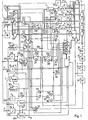
- the basic circuit diagram of the cardiac pacemaker according to the invention shown in block circuit form shown in FIG. 1 shows the signal flow between the individual assemblies and a number of logic operations.
- the pacemaker structure used is based on the concept of a pacemaker, which can be used in different operating modes (modes) due to the switching on and off of signal connections, whereby the switchover between the individual operating modes (the following with the generic ones introduced in the field of pacemaker technology) Codes should be designated) can be programmed and / or signal dependent. In its more complex modes, the pacemaker adapts to the natural heart behavior in a physiological manner.
- the concept shown can also be implemented using discrete or programmable logic components, and in the case of a hardware solution, the required links - as shown - are made using logic gates and storage means such as flip-flops and latches, while, for example, the logic in a microprocessor solution - Decisions are not made in parallel, but serially according to the program.
- RAM memory locations take on the function of the memory means for holding signals that are characteristic of operating states.
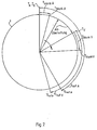
- the starting time T o coincides with the time T A , which is reached after one revolution (corresponding to a cardiac cycle) and characterizes the activity of the atrium.
- a blanking time tbankA follows for the electrode placed in the atrium, the duration of this blanking time depending on whether the stimulation was in the atrium or in the ventricle, ie in the same or in the other chamber. The end of this blanking time is designated T blankA .
- the AV conduction time is between T A and T v , where T v characterizes the time of activity of the ventricle.
- a blanking time t blankV follows accordingly at T v , which ends at the time T blankv .
- the refractory period of the atrium t refA begins at T o and ends at T refA
- the refractory period of the ventricle begins at T v and ends at TreN.
- the times T o g and T tach y cannot be seen directly from the diagram according to FIG. 2, since these are defined as trigger signals by corresponding follow rates of the heart action potentials and / or interference signals.
- connections A and V form inputs and outputs for signals which are picked up by the heart or are given to the heart in the form of stimulation pulses.
- A denotes the connection for an electrode fixed in the atrium and “V” the connection for an electrode fixed in the ventricle.
- the central control for the temporal assignment of the pulses to be emitted takes place via a counter 1, which is incremented by pulses generated by a clock generator 2 and can be reset to an initial position via a “reset” input. Depending on the signals picked up by the heart, this counter can be preset to any counter reading in the forward direction via an additional “preset” input - according to a time advance. It is not necessary to change the counter reading in the reverse direction. After reaching its final value, the subsequent pulse sets the counter to 0, from where the counting process is continued.
- the interaction of the counter with the other components shown in Figure 1 is described in more detail below. (The transmission of individual digital signal pulses or analog signals is shown in the figures by simple connections, while double lines symbolize the transmission of complete data words.)
- the input stage simultaneously effects pulse shaping in such a way that the signals recorded by the atrium can be processed further in the form of pulse-shaped logic signals in the subsequent switching stages.
- the representation of the logic levels in the exemplary embodiment shown takes place in positive logic, that is to say the presence of a signal is denoted by the H state and the absence by the L state. Switching elements (counters, mono and flip-flops) are activated by the rising leading edges of the signal pulses.
- the input stage 101 has filter means, with a Filter characteristics, which preferably make them permeable to the useful signals to be recorded.
- the input stage 101 is also influenced by a blanking circuit 3, which blocks the input stage for predetermined periods t blankA when a stimulation pulse has been delivered to the atrium or ventricle. In this way, it is prevented that a stimulation pulse emitted by the pacemaker is processed as a heart signal and incorrectly influences the operating behavior of the pacemaker.
- a fault detection circuit 102 Downstream of the input stage is a fault detection circuit 102 which emits an output signal when the distance between two successive signal pulses processed by the input stage 101 falls below a predetermined minimum time interval (T o g) corresponding to a maximum repetition frequency.
- T o g predetermined minimum time interval
- Such signals forming a disturbance can be caused both outside (electromagnetic interference or alternating currents) and inside the patient's body (electrode artifacts).
- the interference detection circuit 102 in cooperation with means to be described further below, prevents pulses recorded at the atrium electrode that exceed the predetermined frequency from being permitted for further processing.
- the output of the input stage 101 is also connected to the input of a tachycardia detection stage 103, which correspondingly emits a signal when the pulses appearing at the output of the stage 101 fall below a predetermined subsequent time.
- the “tachycardia rate” T Tach y is approximately 250 ms longer than the time period T o g, which is defined as the criterion for the presence of an interference signal, which is approximately 100 ms.
- connection V to which an electrode to be fixed in the ventricle can be connected, is connected to the input of a further input stage 201, whose basic functions correspond to the input stage 101 for signals received by the atrium.
- the gain factor can be set via an additional input (corresponding arrow P).
- a separate interference detection circuit 202 for the interference signals picked up by the electrode fixed in the ventricle emits an output signal if the signal pulses picked up by the ventricle have a higher frequency than a predetermined frequency.
- the input stage 201 is temporarily blocked accordingly by signals emitted by the blanking stage 3.
- Stimulation pulses for the atrium are generated by means of a pulse shaping circuit 104, the amplitude of the stimulation pulses being adjustable via an additional input (associated arrow P).
- the pulse shaping stage 104 is driven by short-term pulses with a logic H level and also contains the amplification means required to raise the input pulses to the level necessary for stimulation.
- the pulses emitted by the pulse shaping stage 104 arrive on the one hand at connection A and on the other hand to a run-away protection circuit 105, which in the exemplary embodiment shown is formed by a monoflop, the pulse duration of which is matched to the highest permissible stimulation rate in the atrium.
- the protective circuit 105 Upon an output pulse from the pulse shaping stage 104, the protective circuit 105 outputs a pulse of a predetermined width to the inverting input of an AND gate 106, which is then blocked for the duration of the latter pulse for signal pulses arriving at its other input.
- a pulse shaping stage 204 for pulses intended to stimulate the ventricle can also be influenced via a further input (associated arrow P) with regard to the amplitude of the pulses delivered.
- a separate run-away protection circuit 205 for the ventricle blocks an AND gate 206 via its inverting input if the subsequent time of the pulses stimulating the ventricle falls below the predetermined value.
- the comparator circuit 220 emits a signal via an additional output “>” when the counter reading of the counter is greater than the value for T v stored in the memory 221.
- time stamps T A and T v form reference times for the operation of the pacemaker and, in demand operation, end the so-called “escape intervals” within which a corresponding action by the heart prevents the pacemaker from generating a stimulation pulse.
- the times T A and T v for the atrium and ventricle in the memories 121 and 221 are programmed in the form of numerical values which represent those counter readings that the counter 1 must have reached at the time of the stimulation.
- the time allocation to the counter readings takes place in such a way that the stimulation times can be set with a sufficiently fine time grid. With a counter clock of 1 kHz, for example, the available time grid has a division in milliseconds.
- the counter values which can be predetermined by means of the memories 121 or 221 can be changed by means to be shown further below.
- the input pulses for the output stage 104 originate from the output of an OR gate 107, at the inputs of which the signals which are decisive for the delivery of a stimulation pulse to the atrium alternatively arrive.
- One of the inputs of OR gate 107 is connected to the output of an AND gate 108, which is an off emits the output signal when the comparator circuit 120 indicates that the time T A has been reached and thus indicates that in the demand state of the atrial stimulation a time has been reached at which a stimulation pulse is required because the heart is not active.
- the AND gate 108 is switched through via its further input by means of a signal which is emitted from an output “time A” of the operating status register 4 if a pulse output after the expiration of time is desired. If the signal reception is enabled (sens v at block 4) for the corresponding one In this way, the chamber is in “demand” mode with inhibition by its own pulses, while when the signal recording is blocked, stimulation takes place at fixed times.
- Another AND gate 109 is activated via a corresponding output “trig A ” of the circuit 4 when the signal to the atrium is triggered by cardiac actions in the atrium.
- the signal for synchronously triggering the stimulation pulse in the atrium arrives at the input of the AND gate 109 from the output of a further AND gate 110, which in turn is activated when a signal reaches its input from an output “sens A ” of the circuit 4 the recording of signals from the atrium is provided in the selected mode of operation of the pacemaker.
- the AND gate 110 not only receives the output signal of the input stage 101, but also the output signal of a refractory stage for the atrium 5 at its further inverting input, which emits a signal if for a period of time t refA that occurs when the point in time is reached T A corresponding counter reading by counter 1 begins, the processing of the signals recorded in the atrium for evaluation is blocked for the delivery of stimulation pulses.
- a numerical value corresponding to the refractory time T refA for the atrium is stored in a memory 6 and can be changed by external signals using programming means shown below.
- An OR gate 207 and AND gates 208 to 210 form the corresponding logic gates which are decisive for the delivery of stimulation pulses to the ventricle or for the signal recording from the ventricle.
- the desired operating behavior of the pacemaker can also be determined via three outputs "sens v" , "time v” and “trig v " of the circuit 4, the signal reaching the further input of the AND gate 208 releasing the stimulation when the state of the counter 1 corresponds to the counter reading stored in the memory 221 and assigned to the time T v and thus at this time an output signal from the comparator 220 is output to the AND gate 208.
- the synchronous stimulation is triggered by the AND gate 209, to which the output signal of the AND gate 210, which forwards the signal pulses picked up by the ventricle, is fed.
- the AND gate 210 is blocked via its inverting input during the ventricular refractory period treN, which is determined by means of a comparator 7, the count value of the counter 1 reached being compared with the count value stored in the memory 8 and representing the time period T refV and to the content of the memory 8, that of the memory 216, whose content T V "currently normally corresponds to T v , is added.
- the content of the memory 8, like that of the memory 6, can be changed via external programming means.
- the output signals of the AND gates 110 and 210 further influence switches 122 and 222, by means of which the counter 1 uses its preset input to change the values in the memories 121 (for the value T A ) and 221 (for the value T v ) available values can be preset.
- the counter 1 is thus set to the numerical value corresponding to the time T A when an intracardiac signal appears in the atrium or to the numerical value corresponding to the time T v when a signal appears in the ventricle.
- the pacemaker is synchronized with the cardiac behavior when the AND gates 110 and 210 are enabled for signal recording from the heart via their corresponding signal inputs. If the last-mentioned gates are blocked, the stimulation may take place asynchronously.
- One of the switching stages 15 to 20 is actuated by the output signal of the circuit 14, so that the second transmitted partial information arrives in the memory connected to the activated stage of the stages 15 to 20 and is held there.
- the memory levels 4 already mentioned, 6, 8, 9, as well as 121 and 222 record the changeable data essential for the operation of the pacemaker, as they were given in the preceding description.
- the memory 4 can be influenced by additional signals, which originate from the signal processing stage 21, and causes the operating states to be switched depending on signals received by the pacemaker itself from the heart, the input signals of stage 21 originating from stages 102 and 202 and in the atrium or represent interference signals recorded in the ventricle, and from the tachycardia stage 103, which emits an output signal when the tachycardia state has been determined.
- the components for signal processing and storage surrounded by the dash-dotted line are only activated temporarily, since the logic operations required to operate the pacemaker can be carried out in very short times using modern microelectronic components, so that their permanent operation results in unnecessary energy consumption would.
- the components located outside the line mentioned which are either directly connected to the electrodes fixed in the heart and thus control the signal reception from the heart, or the means which form the timer and time comparator means are permanently activated, since the latter determines that at what times logical operations are to be performed.
- the components located within the dash-dotted line are activated by the signals emitted by the comparator means 120 or 220 when a predetermined time has been reached, or by the output signals of the input stages 101 or 201, namely from the heart (outside the respective refractory period) ) a signal was recorded.
- the aforementioned signals are combined via an OR gate 30, which actuates a switch 32 via a monoflop 31, which connects the components arranged within the dash-dotted line in the selected representation to an energy source 33, this “connecting” to an energy source in each time the power supply is increased, that is to say also in a switchover of the components in question from a standby state into an operating state.
- the pulse duration of the monoflop 31 is dimensioned such that a sufficiently long period of time is available to carry out the necessary switching operations.
- Discrete logic components can be operated in an energy-saving manner with such a reduced supply voltage that no changes can be made, but stored signal states are retained. These components are used for subsequent signal processing in the sense that they determine whether a stimulation pulse should be emitted on an input signal or when a predetermined time is reached.
- the arrow E emanating from the energy source 33 which is formed by a battery in the exemplary embodiment shown, indicates that the components arranged outside the dash-dotted line are supplied directly by the energy source 33 without the switching element 32 being interposed.
- the operating functions of conventional pacemaker types with synchronous or asynchronous stimulation in the atrium and / or ventricle can be generated, depending on the state of the switching means 4 and release of the corresponding stimulation signals or signal recording option via the AND gates 108 to 110 or 208 to 210 higher-order pacemaker modes are also possible, such as those in the form of an overview, for example in the article “Physiological Cardiac Pacing”, R. Sutton, J. Perrins and P. Citron in “PACE”; Vol. 3, March-April 1980, pp. 207 to 219 are reproduced.
- the concept shown allows the advantages of a simple, highly reliable system to be combined with such a higher level of processability in such a way that, in the event of a failure of the complex data processing system, a simple replacement system is available, which is able to perform the basic functions of the pacemaker under almost all circumstances to be ensured only by the limited period of operation of the energy sources.
- this equivalent circuit can be activated by various types of signals.
- One of these signals is a signal “Par” emanating from the complex logic circuit, which appears in a logic circuit implemented by means of a microprocessor when within the performed operations, a plausibility error was determined, such as can be generated in a known manner, for example by a parity check with the aid of redundant signals.
- Corresponding signals can also be obtained from circuits working with discrete logic components if additional elements are used here which recognize impermissible operating states, for example in the form of signals, which, for correctly operating logic means, do not, for example, at the same time or not with one above or below a predetermined one Limit frequency, etc. may appear.
- Such signals indicating malfunction are also obtained from the outputs of the run-away protection circuits 105 and 205 and are combined via an OR gate 34.
- the run-away protection circuits may theoretically respond when the clock generator 2 is operating correctly if incorrect values have been read into the memories 121 or 221 due to an error in the part of the logic circuits surrounded by the dash-dotted line .
- a further signal M is supplied to the OR gate 34, which comes from a reed switch which is not shown in the drawing. In this way, it is possible to set the equivalent operating state according to the "magnetic frequency " of the known pacemakers by means of a magnetic field acting from the outside.
- the output of the OR gate 34 activates a memory circuit 35 which contains times T A 'and T v ' corresponding numerical values which are read into the memories 121 and 221 with priority when this memory circuit 35 is activated.
- an output signal is emitted by the circuit 35, which via inverting inputs of AND gates 111 and 211, which are connected between the gates 107 and 106 or 207 and 206 and block this signal path, while the AND gates 112 thus activated and 212 a direct connection is made to the outputs of the comparators 120 and 220.
- the further input of the AND gate is connected to the signal output of the memory 4 which enables the signal recording for the atrium at the AND gate 110. This ensures that synchronization with regular ventricular activity always takes place only with T A and thus the atrium remains in the lead in the case of AV sequential stimulation or the distance between successive points in time T A remains constant in the absence of signal recording from the atrium.
- the pacemaker described here thus ensures the physiologically correct synchronization with the atrium if undisturbed signals are available there. If the signal recording in the atrium is disturbed, a switchover to an operating state that enables signal recording in the ventricle takes place — in accordance with the proposed possibilities of operating state changes, which are described below — so that correct stimulation is also ensured in this case.
- the refractory period of the ventricle is set in a physiologically sensible manner in that it is set despite counter 1 not being synchronized relates to the times at which the heart action was determined in the ventricle, which is realized in the exemplary embodiment shown in that the output signal of the AND gate 210 via an AND gate 214 and a switching element 215 has a memory 216 with one at that time in the counter 1 loaded numerical value, so that this time Tv "can now serve as a reference time for determining the refractory time T refv by the comparator 7.
- the counter is synchronized by the switching element 222 at the time T v , whereby by means of the AND gate 214 in the memory it then transmits that numerical value for T v which is also present in the memory 221.
- the time counter 1 of the pacemaker which is achieved in the illustrated embodiment by the counter 1 being set to the value T v by the switch means 222
- Memory 221 is available is set.
- the blocking of such retrograde conduction is of particular importance because a stimulation pulse in the ventricle emitted by the pacemaker in response to the signal in the atrium with the specified AV conduction time would result in stimulation in the vulnerable phase.
- the signal recording means for the atrium and ventricles are refracted for a predetermined period of time immediately after an extrasystole. That is to say, with an input pulse at AND gate 217, the output of input stage 201 for the ventricle, which appears when comparator 220 also outputs a signal at output ">", which reaches the second input of AND gate 217, becomes a monoflop 218 started. This monoflop then emits an output pulse of approximately 400 ms duration, which reaches an input of the OR gate 219, the second input of which is connected to the output of the comparator 5 for the refractory period T refA , and the output signal of which to one of the inputs of the AND gate 110 is transmitted.
- the refractory time for the atrium is restarted and maintained for the duration of the pulse delivered by the monoflop 218 (preferably 400 ms), so that the pacemaker is synchronized by retrograde Transfers is prevented.
- the disturbance and tachycardia detection means are also blocked for this period, since they should not respond in the event of a retrograde transition.
- the required signal connection is formed by the line from the output of the monoflop 218 to block 3.
- An OR Gate also blocks the ventricle, the time contained in block 7 being able to be used instead of the pulse time of monoflop 218, preferably by means of switching means (not shown).
- the ventricle In the event that signals are recorded simultaneously in the atrium and the ventricle, the ventricle has priority. This ensures that there is initially security against harmful stimulation due to undesired transitions, even if the signal is not clearly identified.
- all changes are carried out at times which do not disturb the operating sequence; these are times at which no stimulation can be effected and also no input signal is expected, the signal reception of which is in turn from the set operating parameters could be dependent.
- Such a point in time is the time range following T v in which both input stages are refractory (cf. FIG. 2, from which the times of the cardiac cycle with regard to the operation of the pacemaker in their basic distribution can be seen).
- T v The period beginning with T v enables the switching operations necessary for the operation of the pacemaker in a manner that least impair the physiological boundary conditions of the stimulation, since switching operations fall into a natural resting period of the heart at this time.
- T v there are also checks that have to be carried out regularly, such as the determination of the operating state of the energy source (EOL block 36).
- the time T v is always run through with normal cardiac behavior and would in itself be sufficient, for example, to adopt the changed operating parameters (corresponding arrow on memory block 4) or to change the programming at this point in time on the basis of the corresponding signals transmitted from the outside (arrow after block 13).
- FIG. 3a shows (in its left area) the detailed circuit of the components 102 and 202 according to FIG. 1 and in its right part a circuit as it forms part of the circuit block 21 in FIG. 1 - this part is for the Processing of input signals from atrium and ventricle available once.
- a delay element 39 has the effect that the pacemaker is not reprogrammed at the time T v until all other functions to be carried out at this time stamp have been carried out.
- the pulses arriving at the input of the circuit in FIG. 3a and coming from the input stages 101 and 201 in FIG. 1 reset a counter 311 which is controlled by clock signals from the clock generator 2 (FIG. 1).
- the counter 311 reaches a counter reading n, it emits an output signal.
- the number n is chosen so that the frequency division of the input clock generated by the counter reading n would produce an output frequency which is equal to the upper limit frequency of the input signals permitted by the pacemaker.
- Input pulses which have a higher rate generate a constant level at the output of blocks 102 and 202, respectively, which indicates the fault condition.
- the output signal n of the counter 311 resets a downstream flip-flop 313 via an AND gate 312 when the pulse is at the other input of the AND gate 312 appears, which resets the counter 311.
- the flip-flop 313 is set via a further AND gate 314, the output “n” of the counter being connected to an inverting input of the AND gate 314. Accordingly, input pulses which exceed the limit rate for interference signals set the flip-flop 313 which is reset by the next pulse, which appears with a longer interval than the interference rate.
- T A The takeover at time T A guarantees that the fault has been correctly recognized and thus a misinterpretation caused by blanking periods is prevented.
- a possibly resulting change in the operating mode then follows at time T v , at the beginning of the refractory period of the ventricle. A fault detection is therefore also possible in principle during the refractory periods with the exception of the blanking times.
- the dash-dotted line shown in FIG. 3a indicates (corresponding to the illustration in FIG. 1) that the counter 311 remains permanently in operation when the circuit parts which can be put into a waiting state to save energy are kept in operation, while the elements to the right of the dash-dotted line only remain as required are activated when the output of the counter outputs a signal to the OR gate 30 in FIG. 1, which triggers an end of the waiting state of the other switching elements.
- a timing signal generated internally in the pacemaker which marks the expiration of a period in which an expected event did not occur, changes the signal processing means in accordance with this result.
- the components 331 to 337 correspond to those labeled 311 to 317 in FIG. 3a, the numbering being carried out in the same sequence.
- the counter 331 counts up to a number p, which is selected such that a pulse sequence time is defined which forms the limit to a pulse rate in the atrium, which characterizes a tachycardia state.
- the following time is 350 ms.
- the reset input of the flip-flop 333 is not directly connected to the output of the AND gate 332, but an OR gate 338 is interposed here, the further input of which is connected to the output of an AND gate 339, the one input of which is in turn is connected to the output of the flip-flop 333.
- the other input of the AND gate 339 is connected to the output of the blanking circuit 3 and receives a signal when the atrium input stage 101 is blocked for signals in response to a stimulation pulse. This ensures that the flip-flop 333 is reset when a stimulation pulse has been emitted and the atrium input stage 101 has been blanked out.
- the selected transfer at the time T A via the further logic means (operating mode memory 4) further ensures that the change in the operating behavior also takes place at a time and in a manner which ensures optimum synchronism with the heart behavior of the patient.
- the determination of the disturbance and tachycardia states in the atrium ensures that both signal states are optimally recorded, whereby by resetting the tachycardia counter during the blanking times alone it is ensured that the disturbance detection is continued independently of it and not by resetting and from it resulting formation of a shortened measuring time interval for the fault detection in connection with the blanking pulses, a fault signal is simulated.
- FIG. 4 shows those components which, on the one hand, allow predetermined operating modes to be programmed by external switching means and which furthermore switch the operating mode in the event of interference pulses arriving at inputs A and V or in the case of tachycardia in the atrium. Particularly noteworthy here is the possibility of selecting the operating mode to be switched on in the event of the occurrence of one or more of the aforementioned events from one or more operating modes defined for this case, and of defining this selection beforehand by programming.
- the circuit arrangement shown in FIG. 4 is the assembly group that is used as the control circuit for the in the block circuit according to FIG Operating modes are combined in one element.
- a (permanent) operating mode of the pacemaker is selected by means of a switching element 400 by means of the programming signal reaching block 4 via the switching element 20, which operating mode is valid when no interference signals are recorded and the tachycardia state is also not present.
- One of the operating modes can be selected by programming.
- further switching elements 401 and 402 can be used to determine which of two alternative operating modes that may be available should come into operation in the event of the occurrence of one or more of the conditions mentioned, switch 401 occurring when various faults occur with respect to a first type and the switch 402 with respect to a second type of interference can be set.
- the assignment selected in the illustrated embodiment can be changed, restricted or expanded depending on the requirements.
- the setting by the switches 401 and 402 in the form shown is not mandatory, but can be changed by additional switching elements in such a way that different alternative operating functions are activated for different fault or tachycardia states.
- OR gates 403 to 408 are alternatively activated (with provisional disregard of the logic components provided for switching on the alternative operating functions), each of which OR Gate 403 to 408 is assigned a flip-flop 413 to 418, at the outputs of which the output signals determining the operating behavior of the pacemaker, which correspond to the output lines of block 4 in FIG. 1, are determined.
- the flip-flop 413 is set or reset in the case of reprogramming by the signal T v , a delay element 419 ensuring that the signals influencing the operating mode, which also takes place at the time T v , are recognized and evaluated are before an operating mode change occurs.
- the criterion for measuring the delay time of the element 419 is that the switching of the operating mode of the pacemaker must be completed within the time during which both inputs A and V are refractory. (It also applies to the other signals triggered by a pulse appearing at time T v that within the entire pacemaker concept shown - depending on the expansion state - there may be an additional delay in signal processing such that such steps are only initiated when the previous processing, which is a prerequisite for these steps, has been completed in the following order: termination of processing for the previous cardiac cycle - operating mode / program change - definition of further data for the next cycle.)
- the flip-flops are switched via AND gates 423 to 428 or 433 to 438, one of the two having the set or reset input of the flip-flops 413 depending on the signal states present at the output of the OR gates 403 to 408 to 418 connected AND gate is activated when the output of the circuit 419 shows the delayed pulse I TV from the time T v .
- the outputs of the OR gates 403 to 408 are each connected to a non-inverting input of one of the AND gates 423 to 428 and an inverting input of the AND gates 433 to 438.
- the time-controlled triggering of atrium pulses is defined by setting the flip-flop 414. Atrium or ventricle signals are not recorded and, as a result, no switchover is necessary in the event of interference signals occurring here .
- the operating modes "AAT” and “AAI” activate when the atrium is undisturbed and, if there is no tachycardia, via AND gates 440 and 441, whose inverting inputs are connected together to the output of an OR gate 442, at the inputs of which these states indicating signals arrive when a fault occurs in the atrium or the tachycardia condition has been determined, the corresponding flip-flops 413 to 415. If a signal with the logic H state is present at the output of OR gate 442, then when « AAT ”or“ AAI ”state via an OR gate 443 and an AND gate 446 and the OR gate 445 the“ A00 ”state is set, as can also be selected directly by appropriate programming.
- the "VVI” operating mode is activated if this State is set via the program switch 400 and there are no disturbances in the ventricle, so that an output signal from the AND gate 447 reaches the OR gate 448. If there is a malfunction in the ventricle, the pacemaker switches to the operating state “V00” by linking the corresponding signals via an OR gate 449, an AND gate 450 and a further OR gate 451.
- the «VAT» operating mode can be set by appropriate programming.
- an OR gate 454 is activated via the AND gate 453 if the AND gate 453 is not blocked by the output signal of the OR gate 442 via its inverting input.
- the system is switched to the «V00» state, which is effected by a line leading to the OR gate, the switching conditions corresponding to those in the « A AT» or «AAI» modes .
- the signal passes through an OR gate 457 to the inputs of two AND gates 458 and 459, the further inputs of which (the further input at the AND gate 458 is inverting) are connected to the output of the switch 401.
- this is set by programming (connection with a logic H level) or not set (corresponding to the logic L level)
- one of the AND gates 458 and 459 is switched through and activated via the AND gate 450 in
- the state “V00” or via the AND gate 460 the further input of which is correspondingly connected to the line carrying a logical “H signal” in the event of a disturbed ventricle, via an OR gate 461 the state «D00».
- the operating state of the pacemaker in this case can be determined by a corresponding presetting.
- the doctor in the event that an operating state of the pacemaker originally selected by him cannot be maintained, can select an alternative state which is particularly favorable in the case of the patient concerned.
- a corresponding option is also provided in the "VDT / I" operating state, the absence of disturbances in the atrium and ventricle and also the absence of the tachycardia state being determined by means of an AND gate 462, the two inverting inputs of which, on the one hand, are connected to the output of the OR -Gatters 442 or with the line indicating a malfunction in the ventricle.
- the output of the AND gate 462 leads to an AND gate 463, the output signal of which triggers the logic operations necessary for the “VDT / I” operating state.
- an OR gate 464 and an AND gate 465 in the presence of a malfunction in the atrium or tachycardia and the presence of a malfunction in the ventricle, either via AND switch 466 or 467, depending on the position of switch 401 the "VVI" state or the "DVI” state activated.
- an AND gate 468 evaluating these signal states, depending on the position of the switch 402, sends a signal to AND gates 469 and 470 as an alternative to the OR gates 451 and 454 , so that in this case the operating states «V00» or «VAT» can be activated alternatively. If the ventricular input signal is disturbed, the attending physician therefore has the option of either still using signals occurring in the atrium to trigger the ventricular stimulation or of stimulating the ventricle at a fixed frequency. The “VDT / 1” operating state thus changes to the “VAT” state, for example.
- the switches are triggered via the OR gate 464 as in the aforementioned operating state, while a corresponding link is also established via the OR gate 457 if the ventricle is disturbed.
- the blanking stage 3 according to FIG. 1 is shown in detail in FIG.
- the output signals of the AND gates 106 and 206 reach the inputs of an OR gate 601, the output signal of which activates a monoflop circuit 602 which emits an output pulse for 25 ms.
- This pulse passes through OR gates 611 and 621 both to the input stage 101 for the atrium and to the input stage 201 for the ventricle and makes both impermeable to incoming signals for this period. Both input stages are blocked for 25 ms regardless of whether a stimulation pulse has been delivered to the atrium or the ventricle.
- the circuit shown also has means which make it possible to distinguish between the stimulated and the non-stimulated chamber with regard to the length of the blanking time.
- the blanking time for the stimulated chamber is increased to ensure that the polarization effects on the electrode have subsided before a new signal can be recorded.
- two monoflop circuits 610 and 620 are provided, which emit an output pulse in response to an input pulse, which corresponds to the extended blanking time for the stimulated chamber - 60 ms in the exemplary embodiment shown.
- the inputs of the monoflop circuits are connected directly to the outputs of the AND gates 106 and 206, while the blanking pulses are each supplied to the second inputs of the OR gates 611 and 621, the activation times being different in the case of stimulation of one of the chambers overlap stages 602 and 620 or 602 and 610 at the output of OR gates 611 and 621.
- the input amplifier is also blocked for the interference signal and tachycardia detection.
Landscapes
- Health & Medical Sciences (AREA)
- Cardiology (AREA)
- Radiology & Medical Imaging (AREA)
- Engineering & Computer Science (AREA)
- Biomedical Technology (AREA)
- Nuclear Medicine, Radiotherapy & Molecular Imaging (AREA)
- Heart & Thoracic Surgery (AREA)
- Life Sciences & Earth Sciences (AREA)
- Animal Behavior & Ethology (AREA)
- General Health & Medical Sciences (AREA)
- Public Health (AREA)
- Veterinary Medicine (AREA)
- Electrotherapy Devices (AREA)
- Measurement And Recording Of Electrical Phenomena And Electrical Characteristics Of The Living Body (AREA)
Claims (7)
Applications Claiming Priority (2)
| Application Number | Priority Date | Filing Date | Title |
|---|---|---|---|
| DE3118100 | 1981-05-04 | ||
| DE3118100 | 1981-05-04 |
Publications (2)
| Publication Number | Publication Date |
|---|---|
| EP0077807A1 EP0077807A1 (fr) | 1983-05-04 |
| EP0077807B1 true EP0077807B1 (fr) | 1987-11-19 |
Family
ID=6131700
Family Applications (1)
| Application Number | Title | Priority Date | Filing Date |
|---|---|---|---|
| EP82901498A Expired EP0077807B1 (fr) | 1981-05-04 | 1982-05-04 | Stimulateur cardiaque |
Country Status (3)
| Country | Link |
|---|---|
| EP (1) | EP0077807B1 (fr) |
| DE (1) | DE3277684D1 (fr) |
| WO (1) | WO1982003782A1 (fr) |
Families Citing this family (3)
| Publication number | Priority date | Publication date | Assignee | Title |
|---|---|---|---|---|
| DE3506791A1 (de) * | 1985-02-22 | 1986-08-28 | Biotronik Meß- und Therapiegeräte GmbH & Co Ingenieurbüro Berlin, 1000 Berlin | Herzschrittmacher mit physiologischer steuerung |
| DE3506789A1 (de) * | 1985-02-22 | 1986-08-28 | Biotronik Meß- und Therapiegeräte GmbH & Co Ingenieurbüro Berlin, 1000 Berlin | Demand-herzschrittmacher mit physiologischer steuerung |
| US5179949A (en) * | 1990-12-07 | 1993-01-19 | Raul Chirife | Cardiac pacemaker with automatic a-v programming for optimization of left heart a-v interval |
Family Cites Families (5)
| Publication number | Priority date | Publication date | Assignee | Title |
|---|---|---|---|---|
| GB1493353A (en) * | 1973-11-21 | 1977-11-30 | Devices Implants Ltd | Device for terminating tachycardia |
| NL7907462A (nl) * | 1978-10-30 | 1980-05-02 | Medtronic Inc | Hartgangmaker. |
| US4312356A (en) * | 1979-03-07 | 1982-01-26 | George Edgar Sowton | Pacemakers for tachycardia control |
| US4280502A (en) * | 1979-08-08 | 1981-07-28 | Intermedics, Inc. | Tachycardia arrester |
| US4485818A (en) * | 1980-11-14 | 1984-12-04 | Cordis Corporation | Multi-mode microprocessor-based programmable cardiac pacer |
-
1982
- 1982-05-04 EP EP82901498A patent/EP0077807B1/fr not_active Expired
- 1982-05-04 DE DE8282901498T patent/DE3277684D1/de not_active Expired
- 1982-05-04 WO PCT/DE1982/000101 patent/WO1982003782A1/fr active IP Right Grant
Also Published As
| Publication number | Publication date |
|---|---|
| DE3277684D1 (en) | 1987-12-23 |
| WO1982003782A1 (fr) | 1982-11-11 |
| EP0077807A1 (fr) | 1983-05-04 |
Similar Documents
| Publication | Publication Date | Title |
|---|---|---|
| DE3145149C2 (fr) | ||
| EP0063097B1 (fr) | Stimulateur cardiaque | |
| EP0399063B1 (fr) | Appareil médical implantable pour stimuler des contractions dans les tissus avec une intensité de stimulation réglable et son procédé d'utilisation | |
| DE3117075C2 (de) | Vorhofsynchroner Herzschrittmacher | |
| DE2006076A1 (de) | Herzschrittmacher | |
| DE2741176A1 (de) | Herzschrittmacher mit automatisch veraenderlichem a-v intervall | |
| DE2823804A1 (de) | Programmierbarer, einpflanzbarer herzschrittmacher | |
| DE3242895A1 (de) | Zweikammer-herzschrittmacher | |
| EP0414928B1 (fr) | Appareil médical de stimulation d'un processus physiologique dans un corps vivant où l'intensité de stimulation est automatiquement adaptée à l'activité corporelle | |
| EP0064940B1 (fr) | Entraîneur cardiaque | |
| EP0077807B1 (fr) | Stimulateur cardiaque | |
| EP0077800B1 (fr) | Stimulateur cardiaque | |
| EP0077806B1 (fr) | Stimulateur cardiaque | |
| EP0077808B1 (fr) | Stimulateur cardiaque | |
| EP0077801B1 (fr) | Stimulateur cardiaque | |
| EP0077799B1 (fr) | Stimulateur cardiaque | |
| DE3217190A1 (de) | Herzschrittmacher | |
| EP0077809B1 (fr) | Stimulateur cardiaque | |
| DE60016452T2 (de) | Herzschrittmacher | |
| DE3217192A1 (de) | Herzschrittmacher | |
| DE3217191A1 (de) | Herzschrittmacher | |
| DE3217199A1 (de) | Herzschrittmacher | |
| DE3217193A1 (de) | Herzschrittmacher | |
| DE3217194A1 (de) | Herzschrittmacher | |
| DE3217195A1 (de) | Herzschrittmacher |
Legal Events
| Date | Code | Title | Description |
|---|---|---|---|
| PUAI | Public reference made under article 153(3) epc to a published international application that has entered the european phase |
Free format text: ORIGINAL CODE: 0009012 |
|
| AK | Designated contracting states |
Designated state(s): DE FR GB NL |
|
| 17P | Request for examination filed |
Effective date: 19830504 |
|
| GRAA | (expected) grant |
Free format text: ORIGINAL CODE: 0009210 |
|
| AK | Designated contracting states |
Kind code of ref document: B1 Designated state(s): DE FR GB NL |
|
| PG25 | Lapsed in a contracting state [announced via postgrant information from national office to epo] |
Ref country code: FR Free format text: THE PATENT HAS BEEN ANNULLED BY A DECISION OF A NATIONAL AUTHORITY Effective date: 19871119 |
|
| REF | Corresponds to: |
Ref document number: 3277684 Country of ref document: DE Date of ref document: 19871223 |
|
| GBT | Gb: translation of ep patent filed (gb section 77(6)(a)/1977) | ||
| EN | Fr: translation not filed | ||
| PLBE | No opposition filed within time limit |
Free format text: ORIGINAL CODE: 0009261 |
|
| STAA | Information on the status of an ep patent application or granted ep patent |
Free format text: STATUS: NO OPPOSITION FILED WITHIN TIME LIMIT |
|
| 26N | No opposition filed | ||
| PG25 | Lapsed in a contracting state [announced via postgrant information from national office to epo] |
Ref country code: GB Effective date: 19890504 |
|
| PG25 | Lapsed in a contracting state [announced via postgrant information from national office to epo] |
Ref country code: NL Effective date: 19891201 |
|
| GBPC | Gb: european patent ceased through non-payment of renewal fee | ||
| NLV4 | Nl: lapsed or anulled due to non-payment of the annual fee | ||
| PGFP | Annual fee paid to national office [announced via postgrant information from national office to epo] |
Ref country code: DE Payment date: 19990521 Year of fee payment: 18 |
|
| PG25 | Lapsed in a contracting state [announced via postgrant information from national office to epo] |
Ref country code: DE Free format text: LAPSE BECAUSE OF NON-PAYMENT OF DUE FEES Effective date: 20010301 |