EP0076157A2 - Protection relay system - Google Patents
Protection relay system Download PDFInfo
- Publication number
- EP0076157A2 EP0076157A2 EP82305149A EP82305149A EP0076157A2 EP 0076157 A2 EP0076157 A2 EP 0076157A2 EP 82305149 A EP82305149 A EP 82305149A EP 82305149 A EP82305149 A EP 82305149A EP 0076157 A2 EP0076157 A2 EP 0076157A2
- Authority
- EP
- European Patent Office
- Prior art keywords
- signal
- electrical
- electrical quantity
- logical state
- protection relay
- Prior art date
- Legal status (The legal status is an assumption and is not a legal conclusion. Google has not performed a legal analysis and makes no representation as to the accuracy of the status listed.)
- Granted
Links
Images


Classifications
-
- H—ELECTRICITY
- H02—GENERATION; CONVERSION OR DISTRIBUTION OF ELECTRIC POWER
- H02H—EMERGENCY PROTECTIVE CIRCUIT ARRANGEMENTS
- H02H3/00—Emergency protective circuit arrangements for automatic disconnection directly responsive to an undesired change from normal electric working condition with or without subsequent reconnection ; integrated protection
- H02H3/40—Emergency protective circuit arrangements for automatic disconnection directly responsive to an undesired change from normal electric working condition with or without subsequent reconnection ; integrated protection responsive to ratio of voltage and current
Definitions
- This invention relates to a protection relay system for an electrical power sysiem.
- Protection relays are classified, according to principle of operation, e.g. electromechanical type relay, static type relay, and digital type relay,
- the electromechanical type relay drives a movable portion by means of flux of magnetic force or electromagnetic force, and opens and closes output contacts by movement of the movable portion.
- the static type relay comprises a transistor circuit wherein comparisons of electrical quantities with one another in terms of magnitude and phases thereof are made, and an output is produced in accordance with result.
- the digital type relay includes such functions as sampling electrical quantites indicative of voltages and currents derived from separate phases of a power system to be protected, holding the respective sampled values, sequentially rearranging the same by means of a multiplexer, converting the rearranged electrical quantities into digital quantities by utilizing an 'analog-to-digital converter, and to processing these digital quantities within a digital processing unit- on the basis of a predetermined relay calculation programs.
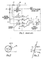
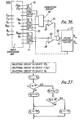
- Figure 1 illustrates a static, type mho characteristic distance relay (hereinafter, simply called a mho relay) for a single phase power system.
- a potential transformer PT and a current transformer CT installed at the terminal of a transmission line TL to be protected, transform voltage and current of the transmission line TL and respectively output a voltage V and a current I in the secondary thereof.
- V and I indicate a voltage vector and a current vector, respectively.
- the voltage V and the current I are respectively supplied to an input conversion unit 100, where they are converted into various electrical quantities such as ⁇ , V ⁇ p and V ⁇ required for mho relay calculation, and are supplied to a relay operation judging unit 200.
- a vector synthesizing circuit AD in the input conversion unit 100 multiplies the current ⁇ by a simulated impedance ⁇ which simulates the line impedance of the transmission line TL so as to produce an electrical quantity ⁇ .
- the phase of the electrical quantity ⁇ leads the phase of the current ⁇ by a line impedance angle (an angle ⁇ ⁇ ).
- ME represents a storage circuit which receives the voltage V and produces an electrical quantity V ⁇ p as a polar quantity.
- the storage circuit ME which comprises for example, a series resonance circuit, produces the electrical quantity V ⁇ p as a damped oscillation so that even if the input voltage abruptly becomes zero the system can maintain a proper judgement for a period of a few cycles.
- a comparator 1 receives the electrical quantity ⁇ at the positive input terminal, and the electrical quantity V ⁇ at the negative input terminal.
- the comparator 1 outputs a logical state "1" when an instantaneous value of ( ⁇ -V ⁇ ) is greater than zero, and when smaller than zero, then outputs a logicl state "0", respectively.
- a comparator 2 similarly receives the electrical quantity V ⁇ p at the positive input terminal, and a DC reference voltage, such as zero volts, electrical quantity at the negative input terminal.
- the DC reference electrical quantity may contain a certain amount of DC bias quantity so as to prevent misoperations of the relay-operation judging unit 200 when no signal is inputted thereto.
- the logical state output signals from the comparators 1 and 2 are inputted to an AND circuit 3, wherein an overlap angle e (overlap time) of the phases of the input signal is detected, and a logical state signal corresponding to the overlap angle ⁇ is produced.
- a time-measuring circuit 4 which comprises an ON-delay timer, outputs a logical state "1" when the period during which the logical state signal "1" from the AND circuit 3 remains is greater than a predetermined period, such as a period corresponding to an electrical angle of 90°.
- the logical state output "1" of the time-measuring circuit 4 indicates that the mho relay is operative, while "0", the mho relay is inoperative.
- the logical state output signal is used to trip a circuit breaker CB provided in the transmission line TL.
- Figure 2 shows a characteristic diagram of the relay shown in Figure 1, which indicates that when an angle defined by the electrical quantities ( ⁇ -V ⁇ ) and V ⁇ p is less than 90°, that is, when the tip of the electrical quantity vector V lies within the circular area, the relay is operated.
- an ohm-characteristic distance relay (hereinafter, simply called ohm relay) which functions as a blinder is utilized together with the mho relay so as to prevent the improper output from being produced in the relay system.
- Figure 3 shows a characterisitc diagram of the ohm relay, which indicates that when an angle ⁇ defined by the electrical quantities ( ⁇ r-V ⁇ ) and ⁇ R is less than 90°, the relay is to be operated.
- the principle structure diagram of the ohm relay is not shown, however, it is similar to that of the mho relay shown in Figure 1 except that the comparators 1 and 2 receive the input electrical quantities ⁇ r and ⁇ R instead of the input electrical quantities ⁇ and V ⁇ p , respectively.
- the invention seeks to provide a protection relay system which is smaller than known systems but uses the hardware of protection relay components which are identical or similar to known components in fundamental principle.
- this invention seeks to provide a protection relay system which is provided to function as a plurality of distance relay components and to judge, by utilizing electrical quantities indicative of voltages and currents derived from an electric power system to be protected, whether the calculated electrical quantities reside within a specified protective region.
- the invention seeks to provide a protection relay system which processes on the basis of simplified digital procedures derived from analogue calculations on a plurality of electrical quantities required for a plurality of distance relay components.
- This invention seeks to provide a protection relay system which can detect a fault in an electric power system having a circuit breaker by using a current and a voltage of the electric power system and cause the circuit breaker to trip in accordance with the fault detection so as to protect the electric power system.
- the invention provides a protection relay system for detecting faults in an electric power system having a circuit breaker, by using a current and a voltage of the electric power system and for causing the circuit breaker to trip if a fault is detected so as to protect the electric power system, the protective relay system, comprising:
- FIG. 4 a block diagram illustrating one embodiment of a protective relaying system according to the present invention.
- This embodiment is provided with functions of three mho relay components which protect transmission lines from short-circuit failures.
- an input conversion unit 100a which is comprised in the same manner as that shown in Figure 1, receives currents of respective phases ⁇ R , ⁇ S and ⁇ T ,and interphase voltages V ⁇ RS , V ⁇ ST and V ⁇ TR , respectively derived from a power system.
- the input conversion system 100a calculates and outputs plural electrical quantities such as ⁇ RS , ⁇ ST , ⁇ TR , V ⁇ PRS , V ⁇ PST and V ⁇ PTR on the basis of well-known calculation procedures, while at the same time, outputs the interphase voltages V ⁇ RS , V ⁇ ST and V ⁇ TR without variations in magnitude and phases thereof, and outputs zero volts (hereinafter written simply as OV).
- ⁇ RS , ⁇ ST and ⁇ TR are electrical quantities indicative of currents which lead the respective currents ( ⁇ R - ⁇ S ) , ( ⁇ S - ⁇ T ) and ( ⁇ T - ⁇ R ) (where, ⁇ R , ⁇ S and ⁇ T represent the line currents on R-phase, S-phase and T-phase, respectively) by the line impedance angle, and V ⁇ pRS , V ⁇ pST and V ⁇ PTR are electrical quantities which are expected to be polar quantities proportional to the respective line voltages.
- V ⁇ TR and zero volts outputted from the input conversion unit 100a are classified into a first group and a second group, and inputted to the relay-operation judging unit 200a.
- the electrical quantities ⁇ RS .... V ⁇ PTR of the first group are inputted to a selecting circuit 5, while the electrical quantities V ⁇ RS .... V ⁇ TR and zero volts cf the second group, to a selecting circuit 6, respectively.
- the selecting circuits 5 and 6 are provided with respective groups of switching elements such as 5-1 .... 5-6 and 6-1 .... 6-4, and when selecting signals in group S51 .... S56 and S61 ....
- a comparator 7 is constructed in the same manner as the comparators 1 and 2 shown in Figure 1, and the positive input terminal thereof is connected to the output terminal of the selecting circuit 5, then the negative input terminal thereof, to the output terminal of the selecting circuit 6, respectively.
- the comparator 7 receives the electrical quantities outputted from the selecting circuits 5 and 6, and compares the same, then outputs thus compared result as a logical state signal.
- Reference numeral 8 designates a microcomputer circuit which is utilized as the digital processing unit.
- the microcomputer circuit 8 has such functions, in brief, as follows; to selectively control the selecting circuits 5 and 6 in a predetermined sequence, to receive and store temporarily the output signal of the comparator 7, which is derived from the result of selection of the selecting circuits 5 and 6, to process the temporarily stored signal in digital procedures, and to judge whether the relay is to be operated. Naturally, the series of operations are executed in accordance with the programs stored previously within the microcomputer circuit 8.
- T M - RS , T M - ST and T M - TR represent respectively the relay-operation judging outputs of the respective phases.
- the microcomputer circuit 8 controls the switching element 5-1 of the selecting circuit 5 so as to select the electrical quantity ⁇ pc , while at the same time, controls the switching element 6-1 of the selecting circuit 6 so as to select the electrical quantity V ⁇ RS .
- the comparator 7 receives the electrical quantities ⁇ FS and V ⁇ RS at the positive and negative input terminals thereof, respectively, and outputs a logical state "1" when (instantaneous value of ⁇ RS ) > (instantaneous value of V ⁇ RS ), and when (instantaneous value of ⁇ RS ) ⁇ (instantaneous value of V ⁇ RS ), then outputs a logical state "0".
- This output signal is temporarily defined as A RS (l).
- the output signal A RS(1) is received in synchronism with the selecting signals by the microcomputer circuit 8.
- the microcomputer circuit 8 controls the switching elements 5- 4 and 6- 4 so as to select the electrical quantities V ⁇ PRS and OV, rcspectively.
- the output of the comparator 7 becomes a logical state "1" when (instantaneous value of V ⁇ p RS ) >OV, and when (instantaneous value of V ⁇ p RS ) ⁇ OV, then becomes a logical state "0".
- This output signal is temporarily defined as B RS (1).
- the output signal B RS (1) is also received in synchronism with the selecting signal by the microcomputer circuit 8.
- signals A ST (1) and B ST (1) on S-T phase, and A TR (1) and B TR (1) on T-R phase are respectively received in the same manner as described above.
- the cyclic repetitions of such control enable the microcomputer circuit 8 to receive the signals such as ARS (2), B RS (2), AST(2), B ST (2), A TR (2), B TR (2), A RS (3), B RS (3) .... B TR (3).
- (1), (2) and (3) indicate the numbers of selecting cycles created by the microcomputer circuit 8 respectively.
- serial signals are processed in digital procedure so as to judge whether the relay is to be operated.
- checking the number of logical states "1" in the serial signals ⁇ A RS (i) ⁇ B RS (i) ⁇ can judge whether a phase angle defined by the electrical quantities ( ⁇ RS -V RS ) and V ⁇ PRS holds a predetermined relationship.
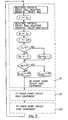
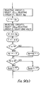
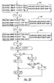
- FIG. 5 is a flowchart illustrating the operations of the microcomputer circuit 8. In this flowchart, the operations which are not directly relevant to the judge of relay operation such as initialization of the microcomputer circuit 8 are omitted.
- the microcomputer circuit 8 causes the selecting circuit 5 to select the electrical quantity ⁇ RS , and the selecting circuit 6, the electrical quantity V ⁇ RS , respectively.
- an input signal IN of the microcomputer circuit 8 becomes A RS (i), and this signal is transferred to a register A.
- the procedure causes the selecting circuit 5 to select the electrical quantity V ⁇ PRS , and the selecting circuit 6, zero volts, respectively.
- the result causes the input signal IN of the microcomputer circuit 8 to be B RS (i), and this signal is transferred to the register B.
- the logical product of the stored contents of registers A and B, A RS (i) ⁇ B RS (i) is obtained, and the result is transferred to a register C.
- the number 90 indicates the number determined from the relationship between an electrical angle of 90° and the number of times of executions in STEP(S1) per an electrical angle of 1° in the foregoing description. Specifically, when an electrical angle is predetermined as of 90° and STEP(S1) through STEP(S3) are executed at a rate of one time per an electrical angle of 1°, by checking whether the count of the counter K R is greater than or equal to 90, it can be judged that whether the phase difference between the two electrical quantities ( ⁇ RS -V ⁇ RS ) and V ⁇ PRS is less than 90°.
- an electrical angle of 90° would correspond to the count of 180 in the counter K R .
- the present invention is not limited to the correlation such as electrical angle of 1° and the count of 90.
- steps following the box discriminating whether the content of the register C is "1" or not is temporarily defined as phase detection subroutine.
- STEPCS2 and STEPCS3 are respectively identical to those of STEP (S1) except that the electrical quantities on R-S phase are substituted by those on S-T phase and T-R phase, respectively.
- the microcomputer circuit 8 cyclically repeats the procedures of STEP (S1), STEP(S2) and STEP (S3).
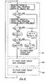
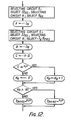
- Figure 6 illustrates the operations of the microcomputer circuit 8 in another example as in a flowchart.
- the operations which are not directly relevant to the relay-operation judgment such as initialization of the microcomputer circuit 8 are also omitted.
- the microcomputer circuit 8 causes the selecting circuits 5 and 6 to select the electrical quantities ⁇ RS and V ⁇ RS , respectively, and as a result, receives the signal A RS (I) as the input signal IN.
- the procedure adds 1 to the count of the counter K R , and when the count of the counter K R is greater than or equal to 90, the procedure causes the output T R to be "I", and when less than 90, causes the output T R to be "0".
- STEP (S12) and STEP (S13) are respectively identical to those of STEP (S11) except that the electrical quantities on R-S phase are substituted by those on S-T phase and T-R phase, respectively.
- the microcomputer circuit 8 repeatedly executes the procedures of STEP (S11) STEP(S12) and STEP (S13).
- Figure 7 (a), 7 (b) and 7 (c) show characteristic diagrams of the embodiment shown in Figure 4. Naturally, the characteristics are identical to those in both the flowcharts in Figures 5 and 6, and are also not limited to those in Figures 5 and 6.
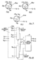
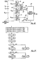
- Figure 8 is a block diagram illustrating the other embodiment wherein the present invention is adapted to a so-called multi-component relay provided with the functions of mho-and ohm-characteristic components.
- a microcomputer circuit 9 provided with such functions that differ from those of the microcomputer circuit 8. All other parts and electrical quantities with identical reference numerals and characters designate the identities in both the drawings.
- Reference numeral 100b designates an input conversion unit which receives the currents ⁇ R and ⁇ S , and the voltage V ⁇ RS and output electrical quantities ⁇ RS , ⁇ rs, V ⁇ PRS , ⁇ Prs and V ⁇ RS and zero volts as a reference voltage.
- the electrical quantities ⁇ RS , V ⁇ p RS and V ⁇ RS are same as those shown in Figure 4 respectively.
- the electrical quantity iZrs is an electrical quantity which is lagged behind the electrical quantity ⁇ RS by a predetermined electrical angle by a well-known phase shifter.
- the electrical quantity ⁇ Prs has the same phase as that of and has the amplitude proportional to that of the electrical quantity ⁇ RS .
- the input electrical quantities of the selecting circuit 5 are ⁇ Z RS , ⁇ Z rs , V ⁇ PRS and ⁇ Z Prs .
- the electrical quantities of the selecting circuit 6 are the line voltages V ⁇ RS and zero volts.
- Reference characters T M - RS and TB-RS designate the outputs of mho relay component and ohm relay component, respectively.
- Figure 9 shows an example of flowcharts of the microcomputer circuit 9.
- Figure 9(a) shows a flowchart corresponding to the mho component, and Figure 9(b), to the ohm component, respectively.
- the microcomputer circuit 9 cyclically repeats these procedures.
- the microcomputer circuit 9 causes the selecting circuit 5 to select the electrical quantity ⁇ rs , and the selecting circuit 6, the electrical quantity VpS, respectively.
- the microcomputer circuit 9 receives a logical state "1" as the input signal IN when an instantaneous value of ( ⁇ rs -V ⁇ RS ) positive, and when negative or zero, then receives a logical state "0".
- the input signal IN is transferred to a register A.
- the microcomputer circuit 9 causes the selecting circuit 5 to select the electrical quantity ⁇ Prs , and the selecting circuit 6, zero volts, respectively.
- the microcomputer circuit 9 receives a logical state "1" as the input signal IN when the instantaneous value of ( ⁇ Prs ) is positive, and when negative or zero, then receives a logi- can state "0".
- the input signal I N is transferred to a register B.
- the procedure adds 1 to the count of the counter K p .
- the procedure causes the count of counter Kp to be 0.
- the count of counter Kp is greater than or equal to 90, the procedure causes the operation judging output T B-RS to be "1", and when less than 90, then causes the output T B-RS to be "0".
- the number 90 is the number determined such that, the same as aforementioned. Namely operations of ohm relay component are executed one time at every electrical angle of 1°, and when a phase angle between the electrical quantities ( ⁇ rs -V ⁇ RS ) and ⁇ Prs lies within 90°, the ohm component is caused to operate.
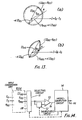
- the characteristics of ohm relay component are shown in vector presentation in Figure 10.
- mho-and ohm relay components have been selectively described, however, distance relay components of various other characteristics, not limited to mho-and ohm characteristics, can also be realized by selecting diversely electrical quantities to be introduced to the inputs of the selecting circuits and contents of the programs stored within the microcomputer circuit.
- Figure 11 shows a structural example of offset mho characteristic distance relay (hereinafter, simply called as offset mho relay) according to another embodiment of this invention.
- offset mho relay the differences from the structure shown in Figure 4 are such that a microcomputer circuit 10 provided with stored programs which are partially different from those of the microcomputer circuit 8 is utilized, and that as an input electrical quantity to a selecting circuit 6, - V ⁇ PRS is introduced. All other parts and electrical quantities with identical reference numerals and characters designate the identities in both the drawings.
- Reference numeral 100c designates an input conversion unit which has the same structure as that of the input conversion unit 100a except that electrical quantities (-1/k) V ⁇ PRS , (-1/k) V ⁇ PST and (-1/k) V ⁇ PTR are outputted instead of the electrical quantities V ⁇ PRS , V ⁇ PST and V ⁇ PTR , respectively.
- a coefficient multiplier which multiplies an input electrical quantity by a factor (-1/k) is too well known to be shown in the input conversion unit 100a.
- the selecting circuits 5 receives the electrical quantities ⁇ RS , ⁇ ST and ⁇ TR .
- the selecting circuit 6 receives the electrical quantities (-1/k) V ⁇ PRS , (-1/k) V ⁇ PST and (-1/k) V ⁇ PTR .
- T OM-RS , T OM-ST and T OM - TR are output signals of the relay.
- the microcomputer circuit 10 causes the selecting circuit 5 to select the electrical quantity ⁇ RS , and the selecting circuit 6, the electrical quantity V ⁇ RS , respectively.
- the microcomputer circuit 10 receives a logical state "1" as the input signal IN when the instantaneous value of ( ⁇ RS -V ⁇ RS ) is positive, and when negative or zero, then receives a logical state "0".
- This input signal IN is transferred to a register A.
- the microcomputer circuit 10 causes the selecting circuit 5 to select the electrical quantity ⁇ RS , the selecting circuit 6, the electrical quantity (- V ⁇ PRS ), respectively.
- the microcomputer circuit 10 receives as the input signal IN a logical state "1" when the instantaneous value of ( ⁇ RS + V ⁇ PRS ) is positive, and'when negative or zero, then receives a logical state "0".
- This input signal IN is transferred to a register B.
- the procedure causes the output T M - RS to be "1", and when less than 90, then causes the output T M - RS to be "0".
- the number 90 is the number determined such that, as the same as described above, when operations of the offset-mho relay component are executed one time at an electrical angle of 1° and a phase angle between the electrical quantities ( ⁇ RS -V ⁇ RS ) and (V ⁇ PRS +K ⁇ RS ) is less than 90°, the procedure causes the component to be operative.
- Figure 13(a) shows a characteristic diagram of the offset-mho relay component shown in Figure 11.
- FIG 14 is a block diagram of the embodiment according to the present invention, wherein RS-phase mho relay component is illustrated.
- reference numeral 100d designates an input conversion unit which receives the current ⁇ R and ⁇ S and the voltage V ⁇ RS and outputs the electrical quantities ⁇ RS , V ⁇ RS and Vp RS and zero volts.
- a selecting circuit 11 is controlled, by selecting signals supplied from a microcomputer circuit 14, to select a single signal from plural input electrical quantities such as ⁇ RS , V ⁇ RS V ⁇ PRS and zero volts so as to output the same.
- a sample-hold circuit 12 is controlled by control signals supplied from the microcomputer circuit 14 so as to sample and hold an output of the selecting circuit 11.
- Reference numeral 13 designates a comparator constructed similarly to the comparator 7.
- a positive input terminal of the comparator 13 is connected to the output terminal of the selecting circuit 11 so as to receive the output electrical quantity thereof.
- a negative input terminal of the comparator 13 is connected to the output terminal of the sample-hold circuit 12 so as to receive the output electrical quantity thereof.
- the microcomputer circuit 14 is provided with such functions as follows : to control concurrently or separately the selecting circuit 11 and the sample-hold circuit 12, to receive and temporarily store a logical state signal outputted from the comparator 13 as the result of such controls, to process the temporarily stored signals in digital procedure, and to judge whether the relay is to be operated. Naturally, these procedures are executed in accordance with the programs stored within the microcomputer circuit 14.
- Reference character T M-RS designates the output of the relaying system.
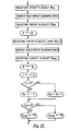
- FIG 15 is an example of flowcharts of the microcomputer circuit 14, whereby the operation thereof will be described.
- the microcomputer circuit 14 firstly causes the selecting circuit 11 to select the electrical quantity V ⁇ RS .
- the selected electrical quantity V ⁇ RS is supplied to the positive input terminal of the comparator 13, while at the same time, also o the sample-hold circuit 12.
- the microcomputer circuit 14 supplies the control signal to the sample-hold circuit 12.so as to sample and hold the electrical quantity V ⁇ RS .
- the output of the sample-hold circuit 12 is supplied to the negative input terminal of the comparator 13. At this instant, the output signal of'the comparator 13 is a logical state "0" .
- the microcomputer circuit 14 causes the selecting circuit 11 to select the electrical quantity ⁇ RS .
- the output of comparator 13 becomes a logical state "L" when the instantaneous value of ( ⁇ RS -V ⁇ RS ) is positive, and when negative or zero, then becomes a logical state "0".
- the microcomputer circuit 14 receives such logical state signals as the input signal I N , and transfers the same to a register A.
- the microcomputer circuit 14 causes the selecting circuit 11 to select zero volts, and supplies the control signal to the sample-hold circuit 12 so as to sample and hold the selected zero volts, then causes the selecting circuit 11 to select the electrical quantity V ⁇ PRS .
- the output of the comparator 13 becomes a logical state "1" when the instantaneous value of V ⁇ PRS is positive, and when negative or zero, then becomes a logical state "0". This is received by the microcomputer circuit 14 and transferred to a register B.
- a logical product of the stored contents of the registers A and B is processed, and the result is transferred to a register C.
- the procedure adds 1 to the count of the counter Kp.
- the procedure causes the count of the counter K R to be 0.
- the procedure causes the output T M-RS to be "L", and when less than 90, then causes the output T M-RS to be "0".
- the number 90 is the number determined such that, as aforementioned, when a phase angle between the electrical quantities ( ⁇ RS -V ⁇ RS ) and V ⁇ PRS is equal to or less than 90°, the component becomes operative.
- Figure 16 shows the other embodiment of the present invention, wherein there are provided an input conversion unit 100e which receives the current ⁇ R and ⁇ S and the voltage V ⁇ RS and outputs the electrical quantities ⁇ RS , (-V ⁇ RS ) and V ⁇ PRS .
- the electrical quantity (-V ⁇ RS ) is the inverse of the electrical quantity V ⁇ RS which is easily obtained from the electrical quantity V ⁇ RS , such as by inverting the polarity of the secondary winding of the transformer, so that an inverting circuit of the electrical quantity V ⁇ RS is not shown in the input conversion unit 100e.
- Selecting circuits 15, 16 and 17 are constructed similarly to the selecting circuits 5 and 6, and have input electrical quantities ⁇ RS , (-V ⁇ RS ) and V ⁇ PRS , respectively.
- a summation circuit 18 receives the outputs of the selecting circuits 15 and 16, and performs summing the received signals so as to produce the summed output.
- Comparators 19 and 20 are constructed similarly to the comparator 7. The positive input terminal of the comparator 19 is connected to the output terminal of the summation circuit 18 so as to receive the output signal thereof. The negative input terminal of the comparator 19 receives zero volts.
- the positive input terminal of the comparator 20 is connected to the output terminal of the selecting circuit 17 so as to receive the output electrical quantity thereof.
- a microcomputer circuit 21 has such functions as follows : to control the selecting circuits 15, 16 and 17 on the basis of the respective predetermined sequence so as to supply predetermined electrical quantities to the respective input terminals of the comparators 19 and 20, to receive and temporarily store a logical state signal of the compared result from the comparators 19 and 20, and to process the temporarily stored signals in digital procedure so as to judge whether the relay is to be operated. Naturally, these procedures are executed in accordance with the programs stored within the microcomputer circuit 21.
- FIG 17 shows an example of flowchart of the microcomputer circuit 21, which illustrates the operations thereof.
- the microcomputer circuit 21 causes the selecting circuits 15, 16 and 17, by applying concurrently selecting signals, to respectively select the electrical quantities ⁇ RS , (-V ⁇ RS ), V ⁇ PRS .
- the summing circuit 18 produces an output of electrical quantity ( ⁇ -V ⁇ RS ) which, inturn, is supplied to the positive input terminal of the comparator 19.
- the comparator 19 When an instantaneous value of ( ⁇ RS -V ⁇ RS ) is positive, the comparator 19 outputs a logical state "1".
- the electrical quantity V ⁇ PRS is applied to the comparator 20, and when an instantaneous value of V ⁇ PRS is positive, the comparator 20 outputs a logical state "1".
- the microcomputer circuit 21 receives the outputs of the comparators 19 and 20 as the input signals I N1 and I N2 , respectively, and transfers the signal I NI to a register A, and the signal I N2 , to a register B, respectively.
- a logical product of the stored contents of the registers A and B is processed, and the result is transferred to a register C.
- the procedure adds 1 to the count of the counter K R .
- the procedure causes the count of the counter K R to be 0.
- the procedure causes the output T M - RS to be "I", and when less than 90, then causes the output T M-RS to be "0".
- the number 90 is the number determined such that, as aforementioned, when a phase angle between the electrical quantities ( ⁇ RS -V ⁇ RS ) and V ⁇ PRS is equal to or less than 90°, the procedure causes the component to be operative.
- Figure 18 (a) is a block diagram of another embodiment according to the present invention, wherein there is procided an amplifier circuit as a variable gain circuit between the selecting circuit and the comparator so as to obtain a first stage reactance characteristic 0 1 and a second stage reactance characteristic 0 2 .
- reference numeral 100f designates an input conversion unit which receives the current ⁇ R , ⁇ S and the voltage V ⁇ RS and outputs electrical quantities ⁇ X and V ⁇ RS .
- 22 and 23 designate selecting circuits constructed similarly to the selecting circuits 5 and 6, with input electrical quantities ⁇ X , .... and V ⁇ RS .... respectively.
- the selecting circuits 22 and 23 are controlled by a microcomputer circuit 26 to select a single signal from plural input electrical quantities such as ⁇ X , .
- V ⁇ RS V ⁇ RS , . . and to output the same.
- the selecting circuits 22 and 23 so as to cope with possible expansion to polyphase types, however, in case of application only to a single phase type, they may be omitted.
- An amplifier circuit 24 has the input terminal connected to the output terminal of the selecting circuit 23, and is constructed so that the gain thereof can be varied depending on a control signal supplied from the microcomputer circuit 26 (described laterl.
- a comparator 25 constructed similarly to the comparator 7 receives the output of the selecting circuit 22 at the - positive input terminal thereof, and the output of the amplifier circuit 24 at the negative input terminal thereof, respectively.
- the microcomputer circuit 26 has such functions as to control the selecting circuits 22 and 23 and the amplifier circuit 24 so as to supply predetermined electrical quantities to the comparator 25, to receive and temporarily store the logical state signal outputted from the comparator 25 as the result of such control, to process the temporarily stored signals in digital procedure, and to judge whether the relay is to be operated. Naturally, these procedures are executed in accordance with the programs stored within the microcomputer circuit 26.
- the amplifier circuit 24 which is utilized as a variable gain circuit may be substituted by an attenuator circuit.
- Figure 19 shows an example of flowcharts of the microcomputer 26, with which the operations thereof will be described.
- the microcomputer circuit 26 firstly causes, by supplying the selecting signals, the selecting circuits 22 and 23 to select electrical quantities ⁇ X and V ⁇ RS , respectively.
- the microcomputer circuit 26 causes, by supplying the control signal, the amplifier circuit 24 to set the gain thereof to a l .
- the output of the comparator 25 becomes "1".
- the microcomputer circuit 26 receives this signal as an input signal I N , and the signal is transferred to a register A.
- the microcomputer circuit 26 causes the amplifier circuit 24 ot set the gain thereof to zero. As a result, when an instantaneous value of ⁇ X is positive, the output of the comparator 25 becomes "1". The microcomputer 26 receives this signal as the input signal IN, and the signal is transferred to a register B.
- a logical product of the stored contents of the registers A and B is processed, and the result is transferred to a register C.
- the procedure adds 1 to the count of the counter K R .
- the procedure causes the count of the counter K R to be 0.
- the procedure causes the output T X1 to be "1", when less than 90, then causes the output T X1 to be "0".
- the number 90 is the number determined such that, as aforementioned, when a phase angle between the electrical quantities ( ⁇ X -V ⁇ RS ) and ⁇ X is within 90°, the procedure cause the component to be operative.
- the characteristic under this condition becomes 01 characteristic shown in Figure 18(b).
- the procedure can cause the amplifier to operate as a selecting circuit.
- this embodiment is not limited to a reactance-type distance relay component, but it is also possible to apply to ohm relay component.
- the microcomputer circuits are disigned to execute digital processing by utilizing only the signals received nearly concurrently.
- This invention is not limited to this, but it is also possible to execute digital processing by utilizing, together with the present input signal, the previously stored signals within storage areas, in which the input signals received previously such a period that corresponds to a predetermined electrical angle prior to the present input signal have been stored.
- Figure 20 shows another embodiment of the present invention.
- 100g is an input conversion unit having the same structure as that of the input conversion unit 100d shown in Figure 14 except that the input conversion unit 100g does not output zero volts.
- a selecting circuit 28 which is constructed similarly to the selecting circuit 5 receives electrical quantities ⁇ RS and V ⁇ PRS from the input conversion unit 100g.
- the selecting ..ircuit 100g is controlled by a control signal supplied from a microcomputer circuit 31 so as to select a single signal from plural input signals thereof, and to output the same.
- An amplifier circuit 29 is constructed similarly to the amplifier circuit 24, is connected to receive the electrical quantity V ⁇ PRS and is controlled by a control signal supplied from the microcomputer circuit 31 so as to vary the gain thereof.
- a comparactor 30 constructed similarly to the comparator 7 receives the output of the selecting circuit 28 at the positive input terminal and the output of the amplifier circuit 29, at the negative input terminal, respectively. The comparator 30 judges that which one of two input electrical quantities is greater than the other, then outputs a logical state signal.
- the microcomputer circuit 31 has such functions as to control the selecting circuit 28 and the amplifier circuit 29 so as to supply predetermined electrical quantities to the comparator 30, to receive and temporarily store a logical state output of the comparator 30 created as a result of such controls, to process the temporarily stored signals in digital procedure, and to judge whether the relay is to be operated.
- reference characters T SU-RS , T 01-RS and T 02 - RS represent relay-operation judging outputs of mho relay component, a first stage reactance relay component and a second stage reactance relay component, respectively.
- Figure 21(a) and 21(bl are an example of flowcharts of the microcomputer circuit 31.
- the microcomputer circuit 31 causes, by supplying selecting signals, the selecting circuit 28 to select the electrical quantity V ⁇ PRS , and concurrently causes, by supplying the control signal, the amplifier circuit 29 to set the gain thereof to Zero.
- the comparator 30 outputs a logical state "1", when negative or zero, the outputs "0".
- the logical state signal is received by the microcomputer circuit 31 as the input signal I N and transferred to a register A.
- the microcomputer circuit 31 causes the selecting circuit 28 to select the electrical quantity ⁇ RS by supplying selecting signals, and causes the amplifier circuit 29 to set the gain thereof the 1/M by supplying control signal. Under this condition, when an instantaneous value of ( ⁇ RS -V ⁇ RS /M) is positive, the output of the comparator 30 becomes "1", and when negative or zero, then becomes "0". This signal is received by the microcomputer circuit 31 as the input signal I N , and transferred to a register B.
- the microcomputer circuit 31 causes, by supplying control signal the amplifier circuit 29 to set the gain thereof to Zero. Under this condition, when an instantaneous value of ⁇ RS is positive, the output of the comparator 30 becomes "l", and when zero or negative, then becomes "0". This signal is received by the microcomputer circuit 31 as the input signal I N , and transferred to a register C.
- the microcomputer circuit 31 causes, by supplying control signal the amplifier circuit 29 to set the gain thereof to 1/X l .
- the output of the comparator 30 becomes "1", and when negative, then becomes or zero, then becomes "0".
- This signal is received by the microcomputer circuit 31 as the input signar I N , then transferred to a register D.
- the microcomputer circuit 31 causes, by supplying control signals, the amplifier circuit 29 to set the gain thereof to 1/X 2 .
- the output of the comparator 30 becomes "1", and when negative, then becomes or zero, then becomes "0".
- This signal is recived by the microcomputer circuit 31 as the input signal I N , then transferred to a register E.
- the microcomputer unit 31 provides a storage area AA of (n+1) bits and controls it in the same manner as a shift register so as to store the previous state of the register D, which is n hits prior to the present state thereof within the register D.
- the number n is defined as the number corresponding to an electrical angle of (90°-(the line impedance angle)l.
- a logical product of the stored content of the registers C and D is processed, and the result is transferred to the register A.
- This logical product stored in the register A becomes "1" when the instantaneous value of the electrical quantity ⁇ RS and the previous instantaneous value of the electrical quantity ( ⁇ RS -V ⁇ RS /X 1 ) which is prior to the present value thereof by an electrical angle of (90°-(the line impedance angle)) are both positive, so that the procedure causes the output T 01-RS to be "1" when the phase angle between both the electrical quantities are within 90° by the phase detection subroutine in the aforementioned manner.
- the microcomputer unit 31 also provides a storage area BB of (n+l) bits and controls it in the same manner as a shift register so as to store the previous state of the register E, which is n bits prior to the present state thereof, within the register E.
- a logical product of the stored contents of the registers C and E is processed, and the result is transferred to the register A.
- the logical product stored in the register A becomes "1" when the instantaneous value of the electrical quantity ⁇ RS and the previous instantaneous value of the electrical quantity ( ⁇ RS -V ⁇ RS /X 2 ) which is prior to the present value thereof by an electrical angle of (90°-(the line impedance angle)) are both positive, so that the procedure causes the output T 02-RS to be "1" when the phase angle between both the electrical quantities are within 90° by the phase detection subroutine in the aforementioned manner.
- Figure 22(a) shows a vector diagram of SU component (mho characteristics) of this embodiment
- Figure 22(b) shows a vector diagram of 0 1 component (reactance characteristics).
- the 0 2 component is identical'to the 0 1 component except the setting thereof, so that description thereof is omitted.
- this reactance characteristic can be realized by holding the angle, which is defined by the electrical quantity which lags behind the electrical quantity ( ⁇ RS -V ⁇ RS /X 1 ) by an electrical angle of ⁇ and the electrical quantity ⁇ RS , within an electrical angle of 90°.
- the register C has a logical state corresponding to the present instantaneous value of the electrical quantity ⁇ RS .
- this reactance characteristic can be realized.
- This embodiment can obtain both characteristics, with only the former current, so that the distance relay with more simplified structure can be realized.
- a combination of two electrical quantities to be judged in terms of phase relationship there between have been utilized to detect whether the phase difference there between lies within a predetermined region.
- such two electrical quantities are selected from the input electrical quantities (such as V ⁇ RS and ⁇ RS ) by means of the selecting circuits (such as reference numerals 5 and 6 in Figure 4) and also from the synthesized electrical quantities of the input electrical quantities (such as ( ⁇ RS -V ⁇ RS ), ( ⁇ RS -V ⁇ RS /M) and ( ⁇ RS -V ⁇ RS /X 1 )).
- Such detection have been made in such manners as follows.
- the procedure selects the instantaneous values of such two electrical quantities so as to supply to the comparators (such as reference numerals 7, 13, 19, 20, 25 and 30).
- the synthesized electrical quantity such as ( ⁇ -V ⁇ RS )
- the synthesized electrical quantity ( ⁇ -V ⁇ RS ) is supplied to one of the two input terminals of the comparator.
- the respective electrical quantities ⁇ RS and V ⁇ RS which constitute the synthesized electrical quantity are respectively supplied to separately different input terminals (i.e. positive and negative input terminals!.
- the procedure detects such phase relationship by checking that the output signal of the comparator (or delayed signal such as in the embodiment shown in Figure 211 maintains continuously the logical state "1" for a certain specified number of times (e.g. the number of times corresponding to an electrical angle of 90°).
- the detection manner according to the present invention is not limited to that described above. A variety of the modified detection manners of phase relationship can also be realized, the modifications thereof will be described hereinafter.
- the step (C ⁇ A ⁇ B, a logical product of the stored contents of the registers A and B is transferred to the register C) may be substituted by the step (C ⁇ A-B, a logical product of the inverses of the stored contents of the registers A and B is transferred to the register Cl, or the step (C ⁇ A ⁇ B+ A ⁇ B , a logical sum of A ⁇ B and A ⁇ B is transferred to the register C) so as to detect the identical phase relationship.
- the respective manners described above are to detect that the coincidence of the output signals of the comparators corresponding to the respective electrical quantities Cor signals delayed from the output signals) has occurred successively for a certain specified number of times.
- the identical phase relationship may be detected by utilizing such manners as follows : in the embodiment shown in Figure 4, for example, the electrical quantity V ⁇ PRS may be substituted by the inversed electrical quantity, (-V ⁇ PRS ); in the flowchart in Figure 5, the step (C ⁇ A ⁇ B) may be substituted by the step (C ⁇ A-B ⁇ , a logical product of the stored content of the register A and the inverse of the stored content of the register B is transferred to the register C) , or by the step (C ⁇ A ⁇ B, a logical product of the inverse of the stored content of the register A and the stored content of the register B is transferred to the register C), or by the step (C ⁇ A ⁇ B+ A ⁇ B , a logical sum of A.B ⁇ and A-B is transferred to the register C).
- the manners to detect the phase relationship are not limited to the above described manners in which the procedure detects whether or not either coincidence or noncoincidence of logical states of two signals continues for a certain specified number of times. Namely, when coincidence of such logical states continues for more than the specified number times (for example, more than the number corresponding to an electrical angle of 90°), naturally noncoincidence of such logical states continues for less than the specified number of times Cfor example, less than the number corresponding to an electrical angle of 90°), so that, by detecting this, the similar phase relationship can be detected.
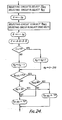
- Figure 23 shows a flowchart on R-S phase according to another embodiment wherein such detection manners described above are utilized in the embodiment shown in Figure 4, and the characteristics similar to STEP Sl in Figure 5 can be obtained.
- the flow up to the step (B ⁇ IN) is similar to that in Figure 5.
- a logic transfer to the register C employs the above described step (C ⁇ A ⁇ B + A ⁇ B), and when the logical states do not coincide, the store content of the register C becomes "1".
- the procedure adds 1 to the count of the counter K R , and causes the count of a counter K N to be 0.
- the procedure adds 1 to the count of the counter K N .
- the above described manner to detect whether or not either coincidence or noncoincidence of the logical states continues for more than the specified number of times also includes the case in which even when such coincidence or noncoincidence does not continue in complete succession, if it can be regarded as substantial continuity, then the procedure detects it assuming that it would continue for more than the specified number of times.
- Figure 24 shows a flowchart indicative of the other embodiment according to the present invention, which may be used in place of STEP Sl in Fugure 5, and where the phase characteristics similar thereto can be obtained.
- This embodiment shows the case when logical procedures are executed at a rate of one time at every electrical angle of 1° of the input electrical quantities.
- the flow up to the step (B ⁇ IN) is similar to that in Figure 5.
- a logic transfer to the register C is made as in the above described manner that is, C ⁇ A.B+A.B, and when the logical states of the registers A and B coincide with each other, either case of "1" or "0", the content of the register C becomes "1".
- the procedure causes the output T M - RS to be "1", and if less than 180, then causes the output T M-RS to be "0".
- the procedure causes the output T M-RS to be "1", and when less than 90, then causes the output T M-RS to be "0".
- the count of the counter K R is to be saturated at 0 and 270, so that once the count has reached 270, it retains 270 even when more additions are made, and also once the count has reached 0, it retains 0 even when more subtractions are made.
- the counter K R When the phase difference of two electrical quantities to be judged in terms of phase relationship is 90°, the counter K R performs additions of 90 times and subtractions of 90 times in the procedure of 180 times during half a cycle of electrical quantities, and although the count deviates in the width of 90 times, the range of deviation is invariable. In the state when the phase difference is greater than or equal to 90°, that is, when the relay is to be inoperative, the number of times of subtractions among the 180 times is greater than the number of times of additions therein, and the count of the counter K R becomes 0.
- the output T M - RS will not be "1", so that even when additions and subtractions of the count are repeatedly made, so long as the relay is in inoperative, the output T M - RS is retained at "0".
- the embodiments according to the present invention include a variety of such manners as to detect the number of times of either coincidence or noncoincidence of logical states of the output signals (or signals delayed therefrom) of the comparators corresponding to the instantaneous values of two electrical quantities to be judged in terms of phase relationship.
- Figure 25 shows a flowchart indicative of another embodiment according to the present invention, which may be utilized in place of STEP Sl of Figure 5, and similar characteristics can be obtained therefrom.
- the flowchart shows the case when digital procedures are made at a rate of one time at every electrical angle of 1° of the input electrical quantities.
- Figure 26 shows a waveform diagram to explain the responding operations in this embodiment.
- a solid-line waveform (i) represents the envelope of the logical state of the register A
- solid-line waveforms (ii), (iii) and (iv) represent the envelopes of the logical states of the register B.
- the logical states of the stored contents of the registers A and B are "1" or "0" only at the instant at which the signals A RS (i) or B RS (i) appears on the input signal IN, however, when illustrated in envelope, they can be represented as square waves which retain for a certain period of time.
- the number of times of succession in logical state "1" on the respective waveforms (i) to (iv) is 180 corresponding to a half cycle of the input electrical quantities, respectively, and the respective dotted lines indicate that whether Kg ⁇ 90 and K B > 90 are held.
- the logical states of the stored contents of the registers A and B are in the relationship between the waveforms (i) and (ii), that is, when the envelope of the logical state of the register B leads the envelope of that of A by 90°, the condition (K A ⁇ 90 and K B > 90) occurs at an instant t l , and the output T M - RS is caused to be "I".
- Figure 26 also shows the phase condition under which the output T M-RS is caused to be "1" in the embodiment shown in Figure 5. Namely, when the logical state of the stored content of the register A lies in the status (i) in Figure 26, if the logical states of the stored content of the register B lie in the statuses (ii), (iii) and (iv), the number of times that both the logical states of the stored contents of the register A and B become "1" reaches greater than or equal to 90, and the output T M - RS is produced. Therefore, the phase condition under which the output T M-RS is caused to be "1" in the embodi- ment shown in Figure 25 is equal to the condition under which the output T M-RS is caused to be "1" in the embodiment shown in Figure 5.
- This embodiment has the manner such that after both the enveloped waveforms of two sequential signals to be judged with respect to phase relationship have been transformed into the dotted line waveforms shown as example in Figure 26, the procedure detects whether the logical states of such signals coincide with "1". As described above, only by detecting whether the specified logical condition holds on the basis of transformation of both the enveloped waveforms of two sequential signals, such a number of times that the enveloped waveform of two sequential signals (include at least one delayed signal therefrom) hold the specified logical condition can be detected.
- the present invention can also be realized by utilizing such manner as described above.
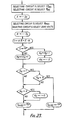
- Figure 27 shows a flowchart of signal processing in the other embodiment of the present invention, which is applied to the embodiment of the structure shown in Figure 20.
- the flow up to the step (D ⁇ IN) is similar to that in Figure 21, so that for simplicity, only the step (D ⁇ IN) is shown, and the steps previous thereto are omitted.
- the signal processing is to be made at a rate of one time at every electrical angle of 1°, and the electrical quantity IZ RS is defined, in this case, as an electrical quantity indicative of a current which leads the current ( ⁇ R - ⁇ S ) by 45°.
- the procedure causes the count of the counter K C to be 46, when is 0, then subtracts 1 from the count of the counter K C .
- the procedure subtracts 1 from the count of the counter K D , and when is 0, then causes the count of the counter K D to be 46.
- the procedure adds 1 to the count of the counter K x , when otherwise, causes the count of the counter K X to be 0.
- the procedure causes the output T X to be "1", when otherwise, causes the output T x to be "0".
- Figure 28 shows a waveform diagram to illustrate the response in the above described embodiment, wherein the phase condition under which the output T SU-RS is caused to be "1" is illustrated.
- the enveloped waveforms such as the solid-line waveform (i) indicative of the stored content of the register A, the dotted-line waveform
- Figure 29 shows a waveform diagram to illustrate the phase condition wherein the output T X is caused to be "1".
- the enveloped waveforms such as the solid-line waveform (i) indicative of the stored content of the register C, the dotted-line waveform (i) indicative of the condition whether the count of the counter K C is greater than or equal to 1 (K C > 1), the solid-line waveforms (ii), (iiil and (iv) indicative of the stored content of the register D, and the dotted-line waveform (ii), (iii) and (iv) indicative of the condition whether the count of the counter K D is greater than or equal to 1 (K D ⁇ ) 1).
- the phase relationship of the enveloped waveform of the register D with respect to the enveloped waveform of the register C is such that it leads by 45° in the waveform (ii), in-phase in the waveform (iii), and lags by 45° in the waveform (iv).
- at least either one of the counts of the counters K C and K D is held greater than or equal to 1 during the entire period, and this is the limit wherein the waveforms (ii) and (iii) hold that status.
- the counter K X is caused to continue to add 1 to the count thereof, which, then, becomes greater than or equal to 400, and the output T X is caused to be "1".
- the status which is not such status that wherein at least either one of the counts of the counters K C or K D is held greater than or equal to 1, inevitably occurs somewhere during every one cycle, so that the count of the counter K X can never be greater than or equal to 400, thus the output T X never become "1". Therefore, when the phase of the enveloped waveform of the register D lies in the range of ⁇ 45° with respect to the enveloped waveform of the register C, the output T X is caused to be "1".
- the status wherein the stored contents of the registers C and D become "1", respectively is the time when the instantaneous values of the respective electrical quantities ⁇ RS and (V ⁇ RS - V ⁇ RS/X1 ) are positive, so that the status wherein the output T X is caused to be "1" is the time when the electrical quantity ( ⁇ RS -V ⁇ RS /X 1 ) lies in the range of ⁇ 45° with respect to the electrical quantity ⁇ RS .
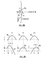
- Figure 30 is a vector diagram illustrating the condition under which the output T M is caused to be "1".
- the vector of the electrical quantity ⁇ RS becomes the vector which leads the current (I R -I S ) by 45° as shown in the diagram.
- a circular arc onm is the locus of the point n at which the vector nm leads by 60° with respect to the vector on (the 7 ector provided with the origin o and the head n)
- a circular arc olm is the circular arc in which the vector lm lags behind the vector ol by 120°.
- the electrical quantity ( ⁇ RS -V ⁇ RS /M) lies in the range of +60° to -120° with respect to the electrical quantity V ⁇ PRS (where the electrical quantity V ⁇ PRS is invariably in-phase to the electri- can quantity V ⁇ RS ) , thus the output T M is caused to be "I".
- Figure 31 shows a vector diagram to illustrate the condition under which the output T X is caused to be "1".
- a two-slope line lmm is parts of the lines provided with an angle of ⁇ 45° with respect to the vector ⁇ RS .
- the electrical quantity ( ⁇ RS -V ⁇ RS /X 1 ) lies in the range of ⁇ 45° with respect to the electrical quantity ⁇ RS , thus the output T X is caused to be "1".
- the manner to obtain the condition under which the output T M is caused to be "1" is made by detection the number of times that a specified logical condition (in this case, coincides with a logical state "1", where the condition (K A ⁇ 60) is defined as "1"), is held.
- the detection is made after transformation of the enveloped waveform of one of the two sequential signals corresponding to the two electrical quantities to be judged in terms of phase relationship thereof.
- the manner to obtain the condition under which the output T X is caused to be "1" is made by detection the number of times that a specified logical condition (in Lhis case, either one of the two is “1", where the conditions (K C ⁇ 1 and K D ⁇ 1) are defined as "1".1 is held.
- the detection is made after transformation of the enveloped waveforms of both the two sequential signals corresponding to the two electrical quantities to be judged in terms of the phase relationship thereof.
- the present invention includes the manner which is made by detection utilizing the number of times that a specified logical condition is held after the various transformation of either one of enveloped waveforms of the sequential signals to be judged in terms of the phase relationship thereof have been made.
- Figure 32 shows a block diagram to illustrate the structure of the other embodiment according to the present invention.
- the structure shown in Figure 32 differs from that of Figure 16 in that there are provided amplifier circuits 24 and 29 between selecting circuits 15 and 16 and a summation circuit 18.
- reference numeral 100h designate an input conversion unit which receives electrical quantities R , S and VRS and outputs electrical quantities ⁇ RS , ⁇ RS and V ⁇ RS and zero volts.
- the electrical quantity ⁇ RS is an electrical quantity indicative of a current which is proportional and in-phase to the current ( ⁇ R - ⁇ S ).
- the selecting circuits 15, 16 and 17 are caused, by selecting signals outputted from a microcomputer circuit 26, to select the electrical quantities ⁇ RS , ⁇ RS and V ⁇ RS , respectively.
- the amplifier circuits 24 and 29 are caused, by control signals outputted from the microcomputer circuit 26, to set the respective gain thereof to X l and R l , thus, output electrical quantities X 1 ⁇ RS and R 1 ⁇ RS, respectively.
- These outputs are supplied to the summation circuit 18 so as to obtain the output of (X 1 ⁇ RS+R 1 ⁇ RS).
- This output and the output V ⁇ RS of the selecting circuit 17 are supplied to the positive and negative input terminals of the comparator 19, respectively.
- step S32 input selection and gain establishment shown in the flowchart permit the comparator 19 to receive the output ⁇ RS of the summation circuit 18 and the output zero volt of the selecting circuit 17, and when the electrical quantity ⁇ RS is positive, the output logical state signal of the comparator 19 becomes "1", and when negative or zero, then becomes "0". This output is received by the microcomputer circuit 26 as the input signal IN, and transferred to a register B. Further, in the following step S33, input selection and gain establishment shown in the flowchart permit the comparator 19 to produce the output of a logical state "1" when the electrical quantity ⁇ RS is positive, and when negative or zero, then to produce a logical state "0". This output is received by the microcomputer circuit 26 as the input signal IN, and transferred to a register C.
- a logical state of (A ⁇ +B+C). (A+B ⁇ +C ⁇ ) is transferred to a register D.
- the procedure adds 1 to the count of the counter K D , further detects whether the count is greater than or equal to 200, and when the count is greater than or equal to 200, then causes the output T X to be "1".
- the count of the counter K D is caused to be 0.
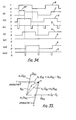
- Figure 34 is a waveform diagram to illustrate the phase conditions under which the output Tx is caused to be "1".
- the waveforms (i) and (ii) represent the enveloped waveforms indicative of the stored contents of the respective registers B and C.
- the waveform of the register B leads the waveform of the register C by 75° (the angle by which the electrical quantity ⁇ RS leads the electrical quantity ⁇ RS , and defined as 75°) and this relationship is invariable.
- the waveforms (iii), (V) and (Vii) respectively represent the enveloped waveforms of the stored content of the register A in the respectively different phases such as when leading the enveloped waveform of the content of the register B by some angles, when lagging behind the enveloped waveform of that of B and leading the enveloped waveform of the of C, and when lagging behind the enveloped waveform of that of C by some angles.
- the waveforms Civl, (Vi) and (Viii) represent the enveloped waveforms of the stored content of the register D in the cases such as when the enveloped waveform of the stored contents of the register.
- A are the waveforms (iii), (V) and (Vii), respectively and for either cases, when the enveloped waveforms of the stored contents of the registers B and C are the waveforms (i) and (ii), respectively.
- the period in which (A+B+C) ⁇ (A+B+C), that is, the stored content of the register D, becomes "0" appears at a rate of one time at every half cycle, as shown in the diagram, so that the count of the counter K D can never be greater than or equal to 200 (a half cycle means 180 timesl, thus the output T X is not caused to be "1".
- Figure 35 shows a vector diagram to illustrate the condition under which the output T X is caused to be "1".
- a two-slope line lmn consists of two liner portions passing the head of the vector (X 1 ⁇ RS+R 1 ⁇ RS) and parallel with the vector ⁇ RS and ⁇ RS .
- the vector V ⁇ RS lies in the operative region defined by the two-slope line lmn as shown, it indicates that the electrical quantity (X 1 ⁇ RS+R 1 ⁇ RS-V ⁇ RS ) lags behind the electrical quantity ⁇ RS , and leads the electrical quantity ⁇ RS , so that the output T X is caused to be "1".
- the system functions to judge the phase relationship between three electrical quantities such as (X 1 ⁇ R S +R 1 ⁇ RS -V ⁇ RS ), ⁇ RS and ⁇ RS , and to detect the judged result by utilizing three sequential signals corresponding to the instantaneous values of such electrical quantities.
- the electrical quantities to be judged in terms of the phase relationship therebetween may be increased in number. For example, four electrical quantities such as (X 1 ⁇ RS +R 1 ⁇ RS -V ⁇ RS ), (X1 ⁇ RS -R 2 ⁇ RS -V ⁇ RS ).
- the procedure judges whether the logical condition (A+B+C+D)-(A+B+C+D) is "1", or whether this logical condition continues greater than or equal to a specified constant number greater than that corresponding to the half cycle of the respective electrical quantities (when signals are processed at a rate of one time at every electrical angle of 1°, for example, 200), then causes the output to be produced.
- a distance relay provided with operation characteristics of quadrilateral characteristic can be obtained, however because of simplicity, detailed descriptions are omitted.
- the present invention includes a variety of manners such that the electrical quantities to be judged in terms of phase relationship are not limited to two in number, but more than two, namely, plural electrical quantities may be judged in the phase relationship thereof by utilizing the logical condition of the plural sequential signals obtained from these electrical quantities.
- Figure 36 shows a block diagram to illustrate the structure of another embodiment according to the present invention.
- reference numeral 100i designates an input conversion unit which receives currents ⁇ R and ⁇ S , a zero-phase current ⁇ O , a voltage V ⁇ RS , a zero-phase voltage Vo and a DC electrical quantity V ⁇ K and outputs electrical quantities ⁇ RS , ⁇ O , (-V ⁇ RS ), V K , V ⁇ PRS and V ⁇ O .
- ⁇ O represents an electrical quantity which is in the constant phase relationship with and proportional to the zero-phase current I O
- V O represents an electrical quantity which is in-phase to and proportional to the zero-phase voltage.
- Reference numeral 32 designates an AND circuit.
- the embodiment in Figure 36 differs from that in Figure 16 only in that the above mentioned electrical quantities are applied, and the output signals of comparators 19 and 20 are supplied to the AND circuit 32, in turn, the output thereof is supplied to a microcomputer circuit 21.
- a logical state of the output T X can be obtained by signal processing similar to that in Figure 17. Namely, the registers A and B are omitted, the microcomputer circuit 21 receives the output signal of the AND circuit 32 as the input signal I N , and transfers this signal to a register C.
- the stored content of i-he register C obtained by such procedure is identical to the content obtained by the flowchart of Figure 17, and thereafter the similar processings are made to cause the output T X to similarly respond.
- Figure 37 shows a flowchart of signal processing to obtain another output T G of embodiment shown in Figure 36.
- the flowchart illustrates that the case signal processings are made at a rate of one time at every electrical angle of 1°.
- the procedure causes the selecting circuits 15, 16 and 17 to select the respective electrical quantities ⁇ O , (-V K ) and V ⁇ O .
- This renders the output of the summation circuit 18 to be the electrical quantity ( ⁇ O -V K ).
- the comparator 19 produces the output signal "1".
- the comparator 20 produces the output signal "1".
- Figure 38 shows a vector diagram to illustrate the condition under the output T G is caused to be "1".
- the output T G is caused to be "1".
- This operative region is defined by such linear portions jk and mn that the in-phase components thereof with respect to the electrical quantity V ⁇ O becomes the electrical quantity and the circular arc klm of the radius V K .
- the operative region is independent of the magnitude of the electrical quantity V ⁇ O .
- Figure 39 is a waveform diagram to illustrate the above-described operation characteristics.
- (i) shows waveforms in the case when the electrical quantity ⁇ O leads the electrical quantity Vo by ⁇ (where, between 45° to 90°), and the operative condition is such that the maximum value of the electrical quantity ⁇ O is greater than the electrical quantity V K during the period between the instant to at which the instantaneous value of V ⁇ O passes across from negative to positive and the instant t 1 at which the instantaneous value of V ⁇ O reaches the maximum value thereof.
- the waveforms (ii) in Figure 39 shows the case when the phase of the electrical quantity ⁇ O lies in the range of ⁇ 45° with respect to that of the electrical quantity V ⁇ O .
- the operative condition becomes such that the instantaneous value of the electrical quantity ⁇ O is greater than the electrical quantity V K during the period of greater than or equal to 90°.
- This condition can be expressed by The limit of this condition is defined as the circular arc klm shown in Figure 38.
- the waveforms (iii) in Figure 39 shows the case when the electrical quantity ⁇ O lags behind the electrical quantity Vo by 6 (where, between 45° to 90°1.
- the operative condition becomes such that the instantaneous value of the electrical quantity ⁇ O is greater than the electrical quantity K A (K A ⁇ 90) during the period between the instant t 1 and the instant t 2 at which the instantaneous value of V ⁇ O passes across from positive to negative.
- This condition can be expressed by an equation similar to the equation (1), and the limit thereof is defined as the line mn shown in Figure 38.
- the instantaneous value of the alternating electrical quantity ⁇ O and the direct current electrical quantity V K are selected by the selecting circuits, and when the instantaneous value of the alternating electrical quantity ⁇ O is greater than the direct current electrical quantity V K (that is, the instantaneous value of ⁇ O lies in a direction more positive than V K ), the sequential signal obtained by the comparator is caused to be "1".
- the embodiment can be executed by such manner as not caly to obtain the sequential signals responding to whether the instantaneous value of the selected alternating electrical quantity is merely positive or negative, but also to obtain the sequential signals reponding to whether such instantaneous value lies within the predetermined range (for example, greater than V K ), and to detect the phase relationship between the enveloped waveforms of these sequential signals and other sequential signals (in this example, those corresponding to V ⁇ O ).
- the present invention includes such embodiment described above.
- the embodiment can be executed not only to respond merely to the ratio of voltages and currents, but also to detect other relationship between voltages and currents, for example, to detect which region the vector of the current ⁇ O resides in with respect to the phase of the voltage V ⁇ O as the reference phase shown in Figure 38, so as to-make a distance relay.
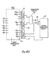
- Figure 40 shows a block diagram to illustrate the structure of another embodiment according to the present invention.
- reference numeral 100j designates an input conversion unit which receives electrical quantities ⁇ R , ⁇ S , V ⁇ RS , V K , V K ⁇ , (-V K ) and ("V K ) and outputs electrical quantities ⁇ RS , V ⁇ PRS , (-V ⁇ RS ) V K , V ⁇ K , (-V K ) and (-V K ) and zero volts.
- the structure shown in Figure 40 is the same as that shown in Figure 16, except as follows:
- the .-utput of the selecting circuit 17 is applied to the negative mput terminal of the comparator 19.
- the comparator 20 is omitted, so that only the output signal of the comparator 19 is received by a microcomputer circuit 21 as the input signal IN.
- the input electrical quantities of,the selecting circuits 15, 16 and 17 are the electrical quantities ⁇ RS and V ⁇ PRS , the electrical quantity (-V ⁇ RS ) and zero volts, and the electrical quantities V K , V K , (-V K ) and (-V K ) and zero volts, respectively, as shown in Figure 40.
- Other parts are identical to those shown in Figure 16.
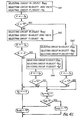
- Figure 41 is a flowchart to illustrate particular steps different from those of other aforementioned embodiments in terms of signal processing.
- the procedure causes the selecting circuits 15, 16 and 17 to select the respective electrical quantities V ⁇ PRS , zero volts and the constant direct current electrical quantity V K .
- the output signal of the comparator 19 is received by the microcomputer circuit 21 as the input signal IN, and transferred to a register A.
- the output signal of the comparator 19 becomes "1"
- the content of. the register A becomes "1" in turn, the procedure moves to a step S43.
- the procedure causes the selecting circuits 15, 16 and 17 to respectively select the electri- can quantity ⁇ RS , (-V RS ) and +V K , and the resultant signal is received as the input signal IN, then transferred to a register Under this condition, when the instantaneous value of the electrical quantity ( ⁇ RS -V ⁇ RS ) is greater than the electrical quantity V K (that is, ⁇ RS -V ⁇ RS >V K ), the stored content of the register C becomes "1".
- step S42 the procedure causes the selecting circuits 15, 16 and 17 to select the electrical quantities V ⁇ PRS , zero volts and (-V K ), respectively, and the resultant signal is received as the input signal IN, then transferred to a register B.
- V PRS electrical quantity
- -V K electrical quantity
- the stored content of the register B becomes "I”.
- the procedure advances to a step S44.
- the procedure causes the selecting curcuits 15, 16 and 17 to select the electrical quantities ⁇ RS , (-V ⁇ RS ) and (-V K ), respectively, and the resultant signal is received as the input signal IN, then transferred to a register D.
- the instantaneous value of the electrical quantity ( ⁇ RS -V ⁇ RS ) is greater than the electrical quantity (-V K ), (that is, ⁇ RS -V ⁇ RS > -V k )
- the stored content of the register D becomes "1".
- the procedure changes the kinds or polarities of electrical quantities to be selected in the following step by the output signal of the comparator 19 in the step S41. This can reduce the number of steps in signal processing, thus can effectively minimize the burdens thereof.
- the system is such that, in the case of a relay provided with certain specified functions, the control procedures of the selecting circuits or amplifier circuits can be made cyclically, so that there are provided,.besides the microcomputer circuit, the control circuits of exclusive use for such control procedures, and by utilizing interrupt commond signals the contents of control are transferred to the microcomputer circuit so as to judge whether the relay is to be operated.
- the present invention essentially numerous different characteristics of relay system can be realized, and there are also provided manners to adequately select the-input electrical quantities, so that the protective relaying system capable of constituting a multi-function relay system provided with various characteristics or a polyphase relay system that performs the relay-operation judgment over specified polyphase can be readily realized smaller in system scale.
Abstract
Description
- This invention relates to a protection relay system for an electrical power sysiem.
- Protection relays are classified, according to principle of operation, e.g. electromechanical type relay, static type relay, and digital type relay,
- The electromechanical type relay drives a movable portion by means of flux of magnetic force or electromagnetic force, and opens and closes output contacts by movement of the movable portion.
- The static type relay comprises a transistor circuit wherein comparisons of electrical quantities with one another in terms of magnitude and phases thereof are made, and an output is produced in accordance with result.
- The digital type relay includes such functions as sampling electrical quantites indicative of voltages and currents derived from separate phases of a power system to be protected, holding the respective sampled values, sequentially rearranging the same by means of a multiplexer, converting the rearranged electrical quantities into digital quantities by utilizing an 'analog-to-digital converter, and to processing these digital quantities within a digital processing unit- on the basis of a predetermined relay calculation programs.
- The static type relay, most commonly used of the three, will be described with reference to the accompanying drawings.
- Figure 1 illustrates a static, type mho characteristic distance relay (hereinafter, simply called a mho relay) for a single phase power system. In Figure 1, a potential transformer PT and a current transformer CT installed at the terminal of a transmission line TL to be protected, transform voltage and current of the transmission line TL and respectively output a voltage V and a current I in the secondary thereof. Here, V and I indicate a voltage vector and a current vector, respectively. The voltage V and the current I are respectively supplied to an
input conversion unit 100, where they are converted into various electrical quantities such as İŻ, V̇p and V̇ required for mho relay calculation, and are supplied to a relayoperation judging unit 200. - A vector synthesizing circuit AD in the
input conversion unit 100 multiplies the current İ by a simulated impedance Ż which simulates the line impedance of the transmission line TL so as to produce an electrical quantity İŻ. Here, the phase of the electrical quantity İŻ leads the phase of the current İ by a line impedance angle (an angle < Ż). ME represents a storage circuit which receives the voltage V and produces an electrical quantity V̇p as a polar quantity. The storage circuit ME, which comprises for example, a series resonance circuit, produces the electrical quantity V̇p as a damped oscillation so that even if the input voltage abruptly becomes zero the system can maintain a proper judgement for a period of a few cycles. - Next, in the relay-
operation judging unit 200, acomparator 1 receives the electrical quantity İŻ at the positive input terminal, and the electrical quantity V̇ at the negative input terminal. Thecomparator 1 outputs a logical state "1" when an instantaneous value of (İŻ-V̇) is greater than zero, and when smaller than zero, then outputs a logicl state "0", respectively. Acomparator 2 similarly receives the electrical quantity V̇p at the positive input terminal, and a DC reference voltage, such as zero volts, electrical quantity at the negative input terminal. The DC reference electrical quantity may contain a certain amount of DC bias quantity so as to prevent misoperations of the relay-operation judging unit 200 when no signal is inputted thereto. The logical state output signals from thecomparators AND circuit 3, wherein an overlap angle e (overlap time) of the phases of the input signal is detected, and a logical state signal corresponding to the overlap angle θ is produced. A time-measuring circuit 4, which comprises an ON-delay timer, outputs a logical state "1" when the period during which the logical state signal "1" from theAND circuit 3 remains is greater than a predetermined period, such as a period corresponding to an electrical angle of 90°. The logical state output "1" of the time-measuring circuit 4 indicates that the mho relay is operative, while "0", the mho relay is inoperative. The logical state output signal is used to trip a circuit breaker CB provided in the transmission line TL. - Figure 2 shows a characteristic diagram of the relay shown in Figure 1, which indicates that when an angle defined by the electrical quantities (İŻ-V̇) and V̇p is less than 90°, that is, when the tip of the electrical quantity vector V lies within the circular area, the relay is operated.
- The foregoing description has been made for a single phase power system, however, for protection of a three-phase circuit, three relays of identical principle and rating should be utilized.
- In the case of the mho relay, when an attempt is made to extend an operative region a load impedance caused by tidal current can possibly penetrate the operative region of the relay.
- In such a case, an ohm-characteristic distance relay (hereinafter, simply called ohm relay) which functions as a blinder is utilized together with the mho relay so as to prevent the improper output from being produced in the relay system.
- Figure 3 shows a characterisitc diagram of the ohm relay, which indicates that when an angle θ defined by the electrical quantities (İŻr-V̇) and İŻR is less than 90°, the relay is to be operated. Here, the principle structure diagram of the ohm relay is not shown, however, it is similar to that of the mho relay shown in Figure 1 except that the
comparators - In conventional static-type protection relay systems, mho relays and ohm relays are individually constituted by separate circuits, and such relays are required to be installed on each phase of the system, such systems have become inevitably bulky in scale, and consequently have disadvantages in terms of maintenance, inspection and cost.
- Accordingly, the invention seeks to provide a protection relay system which is smaller than known systems but uses the hardware of protection relay components which are identical or similar to known components in fundamental principle.
- Second, this invention seeks to provide a protection relay system which is provided to function as a plurality of distance relay components and to judge, by utilizing electrical quantities indicative of voltages and currents derived from an electric power system to be protected, whether the calculated electrical quantities reside within a specified protective region.
- Third, the invention seeks to provide a protection relay system which processes on the basis of simplified digital procedures derived from analogue calculations on a plurality of electrical quantities required for a plurality of distance relay components.
- This invention seeks to provide a protection relay system which can detect a fault in an electric power system having a circuit breaker by using a current and a voltage of the electric power system and cause the circuit breaker to trip in accordance with the fault detection so as to protect the electric power system.
- The invention provides a protection relay system for detecting faults in an electric power system having a circuit breaker, by using a current and a voltage of the electric power system and for causing the circuit breaker to trip if a fault is detected so as to protect the electric power system, the protective relay system, comprising:
- input conversion means adapted for connection to the electric power system to receive a first input signal corresponding to said current and a second input signal corresponding to said voltage, for converting the magnitude and/or the phase of the first and second input signals to produce at least two electrical quantities, and for outputting the unconverted second input signal as an electrical quantity, the resulting plurality of electrical quantities including first, second and third electrical quantities; comparing means'connected to receive the first, second and third electrical quantities for cyclically comparing the first electrical quantity with said second electrical quantity to produce a first logical state signal based on the comparison and comparing the third electrical quantity with a fourth electrical quantity to produce a
- A more complete appreciation of the invention and many of the attendant advantages thereof will be readily obtained as the same become better understood by reference to the following detailed description when considered in connection with the accompanying drawings, wherein:
-
- Figure 1 is a diagram illustrating principle structures of the conventional static-type mho characteristic distance relay;
- Figure 2 is a characteristic diagram of the relay shown in Figure 1;
- Figure 3 is a characteristic diagram of ohm characteristic distance relays;
- Figure 4 is a block diagram illustrating a three-phase mho characteristic short-circuit relay of an embodiment of this invention;
- Figure 5 and Figure 6 are flowcharts illustrating operations of the microcomputer circuit shown in Figure 4;
- Figure 7(a) through 7(c) are characteristic diagrams of the relay shown in Figure 4;
- Figure 8 is a block diagram illustrating a multi-component relay provided with ohm- and mho- characteristics as the other embodiment of the present invention;
- Figure 9(a) and 9(b) are flowcharts illustrating operations of the microcomputer circuit shown in Figure 8;
- Figure 10 is a characteristic diagram of the relay shown in Figure 8;
- Figure 11 is a block diagram illustrating an offset mho characteristic distance relay as another embodiment of the present invention;
- Figure 12 is a flowchart illustrating operations of the microcomputer circuit shown in Figure 11;
- Figure 13(a) and 13(b) are characteristic diagrams of the relay shown in Figure 11;
- Figure 14 is a block diagram illustrating another embodiment of the present invention;
- Figure 15 is a flowchart illustrating operations of the microcomputer circuit shown in Figure 14;
- Figure 16 is a block diagram illustrating the other embodiment of the present invention;
- Figure 17 is a flowchart illustrating operations of the microcomputer circuit shown in Figure 16;
- Figure 18(a) and 18(b) are block diagrams illustrating another embodiment of the present invention and the characteristic diagrams thereof;
- Figure 19 is a flowchart illustrating operations of the microcomputer circuit shown in Figure 18(a);
- Figure 20 is a block diagram illustrating another embodiment of the present invention;
- Figure 21(a) and 2Kb) are flowcharts of operations of the microcomputer circuit shown in Figure 20;
- Figure 22(a) and 22(b) are vector diagrams of mho- and reactance- characteristics of the relay shown in Figure 20;
- Figure 23 through Figure 25 are flowcharts respectively illustrating operations of the microcomputer circuits of the other embodiments of the present invention;
- Figure 26 is a waveform diagram illustrating responses of the flowchart shown in Figure 25;
- Figure 27 is a flowchart illustrating operations of the microcomputer circuit of another embodiment of the present invention;
- Figure 28 and Figure 29 are waveform diagrams illustrating responses of the flowchart shown in Figure 27;
- Figure 30 and Figure 31 are vector diagrams illustrating characteristics of the flowchart shown in Figure 27;
- Figure 32 is a block diagram illustrating the other embodiment of the present invention;
- Figure 33 is a flowchart illustrating operations of the microcomputer circuit shown in Figure 32;
- Figure 34 is a waveform diagram illustrating responses of the microcomputer circuit shown in Figure 32;
- Figure 35 is a vector diagram illustrating characteristics of the microcomputer circuit shown in Figure 32;
- Figure 36 is a block diagram illustrating another embodiment of the present invention;
- Figure 37 is a flowchart illustrating operations of the microcomputer circuit shown in Figure 36;
- Figure 38 is a vector diagram illustrating responses of the microcomputer circuit shown in Figure 36;
- Figure 39(i) through 39(iiil are waveform diagrams illustrating operational characteristics of the microcomputer circuit shown in Figure 36;
- Figure 40 is a block diagram illustrating the other embodiment of the present invention; and
- Figure 41 is a flowchart illustrating operations of the microcomputer circuit shown in Figure 40.
- Referring now to the drawings, wherein like reference numerals designate identical or corresponding parts throughout the several views, and more particularly to Figure 4' thereof, there is shown a block diagram illustrating one embodiment of a protective relaying system according to the present invention. This embodiment is provided with functions of three mho relay components which protect transmission lines from short-circuit failures.
- In Figure 4, an
input conversion unit 100a, which is comprised in the same manner as that shown in Figure 1, receives currents of respective phases İR, İS and İT,and interphase voltages V̇RS, V̇ST and V̇TR, respectively derived from a power system. Theinput conversion system 100a calculates and outputs plural electrical quantities such as İŻRS, İŻST, İŻTR, V̇PRS, V̇PST and V̇PTR on the basis of well-known calculation procedures, while at the same time, outputs the interphase voltages V̇RS, V̇ST and V̇TR without variations in magnitude and phases thereof, and outputs zero volts (hereinafter written simply as OV). Here, the characters marked with dots represent vector quantities, and İŻRS, İŻST and İŻTR are electrical quantities indicative of currents which lead the respective currents (İR-İS) , (İS-İT) and (İT-İR) (where, İR, İS and İT represent the line currents on R-phase, S-phase and T-phase, respectively) by the line impedance angle, and V̇pRS, V̇pST and V̇PTR are electrical quantities which are expected to be polar quantities proportional to the respective line voltages. The plural electrical quantities İŻRS, İŻST.... V̇TR and zero volts outputted from theinput conversion unit 100a are classified into a first group and a second group, and inputted to the relay-operation judging unit 200a. The electrical quantities İŻRS .... V̇PTR of the first group are inputted to a selectingcircuit 5, while the electrical quantities V̇RS .... V̇TR and zero volts cf the second group, to a selectingcircuit 6, respectively. The selectingcircuits circuits digital processing unit 8. - A
comparator 7 is constructed in the same manner as thecomparators circuit 5, then the negative input terminal thereof, to the output terminal of the selectingcircuit 6, respectively. Thecomparator 7 receives the electrical quantities outputted from the selectingcircuits -
Reference numeral 8 designates a microcomputer circuit which is utilized as the digital processing unit. Themicrocomputer circuit 8 has such functions, in brief, as follows; to selectively control the selectingcircuits comparator 7, which is derived from the result of selection of the selectingcircuits microcomputer circuit 8. - In Figure 4, TM-RS, T M-ST and TM-TR represent respectively the relay-operation judging outputs of the respective phases.
- Nextly, the operations of the first embodiment according to the present invention will be described. First, the method in which the
microcomputer circuit 8 controls the selectingcircuits comparator 7 will be described. - The
microcomputer circuit 8 controls the switching element 5-1 of the selectingcircuit 5 so as to select the electrical quantity İŻpc, while at the same time, controls the switching element 6-1 of the selectingcircuit 6 so as to select the electrical quantity V̇RS. As a result, thecomparator 7 receives the electrical quantities İŻFS and V̇RS at the positive and negative input terminals thereof, respectively, and outputs a logical state "1" when (instantaneous value of İŻRS) > (instantaneous value of V̇RS), and when (instantaneous value of İŻRS) < (instantaneous value of V̇RS), then outputs a logical state "0". This output signal is temporarily defined as ARS(l). The output signal ARS(1) is received in synchronism with the selecting signals by themicrocomputer circuit 8. Next, similarly themicrocomputer circuit 8 controls the switching elements 5-4 and 6-4 so as to select the electrical quantities V̇PRS and OV, rcspectively. Under this condition, the output of thecomparator 7 becomes a logical state "1" when (instantaneous value of V̇pRS) >OV, and when (instantaneous value of V̇pRS) < OV, then becomes a logical state "0". This output signal is temporarily defined as BRS(1). The output signal BRS(1) is also received in synchronism with the selecting signal by themicrocomputer circuit 8. - Subsequently, signals AST(1) and BST (1) on S-T phase, and ATR(1) and BTR(1) on T-R phase are respectively received in the same manner as described above.
- Furthermore, the cyclic repetitions of such control enable the
microcomputer circuit 8 to receive the signals such as ARS (2), BRS (2), AST(2), BST(2), ATR(2), BTR(2), ARS(3), BRS(3) .... BTR(3). Here (1), (2) and (3) indicate the numbers of selecting cycles created by themicrocomputer circuit 8 respectively. The sequencial signals can be obtained in synchronism with the operations of the selectingcircuits - In this embodiment, the serial signals are processed in digital procedure so as to judge whether the relay is to be operated.
- Now, with attention to R-S phase, the operations thereof will be described, hereinafter.
- The signal ARS(i), as described above, becomes a logical state "1" when (instantaneous value of İŻRS)> (instantaneous value of V̇RS), that is, when (instantaneous value of (İŻRS- V̇RS)) > OV. The signal BRS(i), as described above, becomes a logical state "1" when (instantaneous value of VppS) > OV. This causes the logical product ARS(i)·BRS(i) to become "1" when both the instantaneous values of the electrical quantities (İŻRS-VRS) and V̇PRS are positive.
- Therefore, checking the number of logical states "1" in the serial signals {ARS(i)·BRS(i)} can judge whether a phase angle defined by the electrical quantities (İŻRS-VRS) and V̇PRS holds a predetermined relationship.
- Namely, assuming that the serial signals {ARS(i)·BRS(i)} are obtained at every electrical angle of 1°, for example, by checking whether the serial signals consecutively maintain logical state "1" for more than or equal to 90 times, it can be judged that whether a phase difference between the electrical quantities (İŻRS-V̇RS) and V̇PRS lies within an electrical angle of 90°.
- In this case, it is obvious that the characteristics of the relay will be mho characteristics, the same as those shown in Figure 2.
- Figure 5 is a flowchart illustrating the operations of the
microcomputer circuit 8. In this flowchart, the operations which are not directly relevant to the judge of relay operation such as initialization of themicrocomputer circuit 8 are omitted. - In STEP (S1) as shown in Figure 5, the
microcomputer circuit 8 causes the selectingcircuit 5 to select the electrical quantity İŻRS, and the selectingcircuit 6, the electrical quantity V̇RS, respectively. As a result, an input signal IN of themicrocomputer circuit 8 becomes ARS(i), and this signal is transferred to a register A. Next, the procedure causes the selectingcircuit 5 to select the electrical quantity V̇PRS, and the selectingcircuit 6, zero volts, respectively. The result causes the input signal IN of themicrocomputer circuit 8 to be BRS (i), and this signal is transferred to the register B. Next, the logical product of the stored contents of registers A and B, ARS(i)·BRS(i) is obtained, and the result is transferred to a register C. Here, in the case when a logical product holds, the case is defined as C="1", and in the case when a logical product does not hold, then the case is defined as C="0". Nextly, when the stored content of register C is in "0", the procedure causes the count of counter KR to be 0, and when the stored content of register C is in "1", the procedure adds 1 to the count of the counter KR. Next, when the count of the counter KR is greater than or equal to a predetermined count, such as 90, the procedure causes the output TM-RS to be "1", and when less than 90, then causes the output T M-RS to be "0". - Here, the
number 90 indicates the number determined from the relationship between an electrical angle of 90° and the number of times of executions in STEP(S1) per an electrical angle of 1° in the foregoing description. Specifically, when an electrical angle is predetermined as of 90° and STEP(S1) through STEP(S3) are executed at a rate of one time per an electrical angle of 1°, by checking whether the count of the counter KR is greater than or equal to 90, it can be judged that whether the phase difference between the two electrical quantities (İŻRS-V̇RS) and V̇PRS is less than 90°. - Therefore, provided STEP(Sl) be executed at a rate of one time per an electrical angle of 0.5°, an electrical angle of 90° would correspond to the count of 180 in the counter KR. Namely, the present invention is not limited to the correlation such as electrical angle of 1° and the count of 90. Here, in STEP(S1), steps following the box discriminating whether the content of the register C is "1" or not is temporarily defined as phase detection subroutine.
- The operations of STEPCS2) and STEPCS3) are respectively identical to those of STEP (S1) except that the electrical quantities on R-S phase are substituted by those on S-T phase and T-R phase, respectively. The
microcomputer circuit 8 cyclically repeats the procedures of STEP (S1), STEP(S2) and STEP (S3). - Figure 6 illustrates the operations of the
microcomputer circuit 8 in another example as in a flowchart. In the flowchart, the operations which are not directly relevant to the relay-operation judgment such as initialization of themicrocomputer circuit 8 are also omitted. - In STEP (S11) as shown in Figure 6, the
microcomputer circuit 8 causes the selectingcircuits - When this signal is "0", the procedure causes the count of counter KR to be 0, causes the output TM-RS to be "0", and executes the following STEP(S12). On the other hand, when the input signal IN is "1", the
microcomputer circuit 8 causes the selectingcircuit 5 to select the electrical quantity VpRS, and the selectingcircuit 6, zero volts, respectively. This result develops the signal BRS (i) on the input signal IN. When this signal is "0", the procedure causes the count of counter KR to be 0, causes the output TM-RS to be "0", and executes the following STEP(S12). When the input signal IN is "1", the procedure adds 1 to the count of the counter KR, and when the count of the counter KR is greater than or equal to 90, the procedure causes the output TR to be "I", and when less than 90, causes the output TR to be "0". - The operations of STEP (S12) and STEP (S13) are respectively identical to those of STEP (S11) except that the electrical quantities on R-S phase are substituted by those on S-T phase and T-R phase, respectively. The
microcomputer circuit 8 repeatedly executes the procedures of STEP (S11) STEP(S12) and STEP (S13). - Figure 7 (a), 7 (b) and 7 (c) show characteristic diagrams of the embodiment shown in Figure 4. Naturally, the characteristics are identical to those in both the flowcharts in Figures 5 and 6, and are also not limited to those in Figures 5 and 6.
- As described above, according to the embodiment of the present invention, plural relays which are identical to each other in fundamental principle structure and installed on respective phases can be substituted by a single relay with the above-described simplified structure, therefore, the protective relaying system can effecitively achieve reduction in system scale.
- Nextly, another embodiment according to the present invention will be described. Figure 8 is a block diagram illustrating the other embodiment wherein the present invention is adapted to a so-called multi-component relay provided with the functions of mho-and ohm-characteristic components. In Figure 8, only a part which differs from the structure of the protective relaying system shown in Figure 4 is a
microcomputer circuit 9 provided with such functions that differ from those of themicrocomputer circuit 8. All other parts and electrical quantities with identical reference numerals and characters designate the identities in both the drawings. -
Reference numeral 100b designates an input conversion unit which receives the currents İR and İS, and the voltage V̇RS and output electrical quantities İŻRS, İŻrs, V̇PRS, İŻPrs and V̇RS and zero volts as a reference voltage. Here, the electrical quantities İŻRS, V̇pRS and V̇RS are same as those shown in Figure 4 respectively. The electrical quantity iZrs is an electrical quantity which is lagged behind the electrical quantity İRS by a predetermined electrical angle by a well-known phase shifter. The electrical quantity İŻPrs has the same phase as that of and has the amplitude proportional to that of the electrical quantity İŻRS. - The input electrical quantities of the selecting
circuit 5 are İZRS, İZrs, V̇PRS and İZPrs. The electrical quantities of the selectingcircuit 6 are the line voltages V̇RS and zero volts. Reference characters TM-RS and TB-RS designate the outputs of mho relay component and ohm relay component, respectively. - Nextly, the operations of this embodiment will be described. Figure 9 shows an example of flowcharts of the
microcomputer circuit 9. Figure 9(a) shows a flowchart corresponding to the mho component, and Figure 9(b), to the ohm component, respectively. Themicrocomputer circuit 9 cyclically repeats these procedures. - Now, the operations of the mho component in Figure 9(a) are identical to those of STEP(Sl) shown in Figure 5, so that the description of its operations is omitted. In Figure 9(b), the
microcomputer circuit 9 causes the selectingcircuit 5 to select the electrical quantity İŻrs, and the selectingcircuit 6, the electrical quantity VpS, respectively. As a result, themicrocomputer circuit 9 receives a logical state "1" as the input signal IN when an instantaneous value of (İŻrs-V̇RS) positive, and when negative or zero, then receives a logical state "0". The input signal IN is transferred to a register A. - Next, the
microcomputer circuit 9 causes the selectingcircuit 5 to select the electrical quantity İŻPrs, and the selectingcircuit 6, zero volts, respectively. As a result, themicrocomputer circuit 9 receives a logical state "1" as the input signal IN when the instantaneous value of (İŻPrs) is positive, and when negative or zero, then receives a logi- can state "0". The input signal IN is transferred to a register B. - Nextly, the logical product of the stored contents of the registers A and B is obtained, and the result such as a logical state "1" or "0" is transferred to a register C. Next, when the content of the register C is "1", that is, when both the instantaneous values of the electrical quantities (İŻrs-V̇RS) and İŻPrs are positive, the procedure adds 1 to the count of the counter Kp. When the content of the register C is "0" the procedure causes the count of counter Kp to be 0. Next, the count of counter Kp is greater than or equal to 90, the procedure causes the operation judging output TB-RS to be "1", and when less than 90, then causes the output TB-RS to be "0". Here, the
number 90 is the number determined such that, the same as aforementioned. Namely operations of ohm relay component are executed one time at every electrical angle of 1°, and when a phase angle between the electrical quantities (İŻrs-V̇RS) and İŻPrs lies within 90°, the ohm component is caused to operate. The characteristics of ohm relay component are shown in vector presentation in Figure 10. - As described above, according to the embodiment of the present invention, plural relay components having similarities in fundamental principle structure can be substituted by a single relay with the above described simplified structure, therefore, this effectively contributes to reduction in system scale for the protective relaying system.
- In the aforementioned embodiments of the present invention, mho-and ohm relay components have been selectively described, however, distance relay components of various other characteristics, not limited to mho-and ohm characteristics, can also be realized by selecting diversely electrical quantities to be introduced to the inputs of the selecting circuits and contents of the programs stored within the microcomputer circuit.
- Next, one example of such distance relay will be described. Figure 11 shows a structural example of offset mho characteristic distance relay (hereinafter, simply called as offset mho relay) according to another embodiment of this invention. In Figure 11, the differences from the structure shown in Figure 4 are such that a
microcomputer circuit 10 provided with stored programs which are partially different from those of themicrocomputer circuit 8 is utilized, and that as an input electrical quantity to a selectingcircuit 6, -
-
Reference numeral 100c designates an input conversion unit which has the same structure as that of theinput conversion unit 100a except that electrical quantities (-1/k) V̇PRS, (-1/k) V̇PST and (-1/k) V̇PTR are outputted instead of the electrical quantities V̇PRS, V̇PST and V̇PTR, respectively. Here a coefficient multiplier which multiplies an input electrical quantity by a factor (-1/k) is too well known to be shown in theinput conversion unit 100a. The selectingcircuits 5 receives the electrical quantities İŻRS, İŻST and İŻTR. The selectingcircuit 6 receives the electrical quantities (-1/k) V̇PRS, (-1/k) V̇PST and (-1/k) V̇PTR. TOM-RS, TOM-ST and TOM-TR are output signals of the relay. - The operations of the above described embodiment will be explained with reference to Figure 12, wherein an example of flowchart, relating to RS-phase only, of the
microcomputer circuit 10 is illustrated. First, themicrocomputer circuit 10 causes the selectingcircuit 5 to select the electrical quantity İŻRS, and the selectingcircuit 6, the electrical quantity V̇RS, respectively. As a result, themicrocomputer circuit 10 receives a logical state "1" as the input signal IN when the instantaneous value of (İŻRS-V̇RS) is positive, and when negative or zero, then receives a logical state "0". This input signal IN is transferred to a register A. - Next, the
microcomputer circuit 10 causes the selectingcircuit 5 to select the electrical quantity İŻRS, the selectingcircuit 6, the electrical quantity (-
microcomputer circuit 10 receives as the input signal IN a logical state "1" when the instantaneous value of (İŻRS+
- Nextly, a logical product of the stored contents of the registers A and B is processed, and the result is transferred to a register C. Next, when the content of the register C is "l", that is, when both the instantaneous values of the electrical quantities (İŻRS-V̇RS) and (V̇PRS+KİŻRS) are positive, the procedure adds 1 to the count of the counter KR. When the stored content of the register C is "0", the procedure causes the count of counter KR to be 0.
- Next, when the count of the counter KR is greater than or equal to 90, the procedure causes the output TM-RS to be "1", and when less than 90, then causes the output TM-RS to be "0". Here, the
number 90 is the number determined such that, as the same as described above, when operations of the offset-mho relay component are executed one time at an electrical angle of 1° and a phase angle between the electrical quantities (İŻRS-V̇RS) and (V̇PRS+KİŻRS) is less than 90°, the procedure causes the component to be operative. Figure 13(a) shows a characteristic diagram of the offset-mho relay component shown in Figure 11. - In the above described embodiment, when the count of the counter KR is greater than or equal to 135, the procedure causes the output TOM-RS to be "I", and when less than 135, then causes the output TOM-RS to be "0". This results in that when a phase angle between the electrical quantities (İŻRS-V̇RS) and (V̇PRS+KİŻRS), is less than or equal to 45°, the component becomes operative, so that a convex lens (a two- circular arcl characteristic is obtained, as shown in Figure 13(b).
- In the aforementioned embodiment shown in Figure 11, only a structural example of offset mho relay has been described, but also a reactance characteristic distance relay can readily be realized. Moreover, it is also possible to utilize the judging unit in common for polyphase or multi-component relay application.
- In the emboidments of the present invention described above, the two selecting circuits have been utilized, however, this invention, as shown in Figure 14, can reduce the number of selecting circuits by adopting a sample-hold circuit together with a single selecting circuit. Figure 14 is a block diagram of the embodiment according to the present invention, wherein RS-phase mho relay component is illustrated.
- In Figure 14,
reference numeral 100d designates an input conversion unit which receives the current İR and İS and the voltage V̇RS and outputs the electrical quantities İŻRS, V̇RS and VpRS and zero volts. A selectingcircuit 11 is controlled, by selecting signals supplied from amicrocomputer circuit 14, to select a single signal from plural input electrical quantities such as İŻRS, V̇RS V̇PRS and zero volts so as to output the same. A sample-hold circuit 12 is controlled by control signals supplied from themicrocomputer circuit 14 so as to sample and hold an output of the selectingcircuit 11.Reference numeral 13 designates a comparator constructed similarly to thecomparator 7. A positive input terminal of thecomparator 13 is connected to the output terminal of the selectingcircuit 11 so as to receive the output electrical quantity thereof. On the other hand, a negative input terminal of thecomparator 13 is connected to the output terminal of the sample-hold circuit 12 so as to receive the output electrical quantity thereof. Themicrocomputer circuit 14 is provided with such functions as follows : to control concurrently or separately the selectingcircuit 11 and the sample-hold circuit 12, to receive and temporarily store a logical state signal outputted from thecomparator 13 as the result of such controls, to process the temporarily stored signals in digital procedure, and to judge whether the relay is to be operated. Naturally, these procedures are executed in accordance with the programs stored within themicrocomputer circuit 14. Reference character TM-RS designates the output of the relaying system. - Figure 15 is an example of flowcharts of the
microcomputer circuit 14, whereby the operation thereof will be described. Themicrocomputer circuit 14 firstly causes the selectingcircuit 11 to select the electrical quantity V̇RS. The selected electrical quantity V̇RS is supplied to the positive input terminal of thecomparator 13, while at the same time, also o the sample-hold circuit 12. Nextly, themicrocomputer circuit 14 supplies the control signal to the sample-hold circuit 12.so as to sample and hold the electrical quantity V̇RS. The output of the sample-hold circuit 12 is supplied to the negative input terminal of thecomparator 13. At this instant, the outputsignal of'the comparator 13 is a logical state "0" . - Next, the
microcomputer circuit 14 causes the selectingcircuit 11 to select the electrical quantity İŻRS. Under this condition, the output ofcomparator 13 becomes a logical state "L" when the instantaneous value of (ŻRS-V̇RS) is positive, and when negative or zero, then becomes a logical state "0". Themicrocomputer circuit 14 receives such logical state signals as the input signal IN, and transfers the same to a register A. - Nextly, the
microcomputer circuit 14 causes the selectingcircuit 11 to select zero volts, and supplies the control signal to the sample-hold circuit 12 so as to sample and hold the selected zero volts, then causes the selectingcircuit 11 to select the electrical quantity V̇PRS. As a result, the output of thecomparator 13 becomes a logical state "1" when the instantaneous value of V̇PRS is positive, and when negative or zero, then becomes a logical state "0". This is received by themicrocomputer circuit 14 and transferred to a register B. - Next, a logical product of the stored contents of the registers A and B is processed, and the result is transferred to a register C. Next, when the stored content of register C is "1", that is, when both the instantaneous values of the electrical quantities (İŻRS-V̇RS) and V̇PRS are positive, the procedure adds 1 to the count of the counter Kp. When the stored content of the register C is "0", the procedure causes the count of the counter KR to be 0.
- Next, when the count of the counter KR is greater than or equal to 90, the procedure causes the output TM-RS to be "L", and when less than 90, then causes the output TM-RS to be "0". Here, the
number 90 is the number determined such that, as aforementioned, when a phase angle between the electrical quantities (İŻRS-V̇RS) and V̇PRS is equal to or less than 90°, the component becomes operative. - This characteristic becomes identical (though a single phase) to the mho characteristic shown in Figure 7.
- Even when such a single selecting circuit is utilized, it is obvious that the following characteristics can be realized by diversifying the electrical quantities to be inputted to the selecting circuit and the programs to preciously be stored within the
microcomputer circuit 14. -
- (1) Various characteristics such as ohm-, reactance-, and offset mho-characteristics which can be obtained by varying diversely the input electrical quantities of the
comparators - (2) Characteristics of polyphase input-type relay same as the characteristics of the relay shown in Figure 4.
- (3) Characteristics of multi-component-type relay same as the characteristics of the relay shown in Figure 8.
- In aforementioned embodiments, such structures wherein no analog operation processing are executed between the selecting circuits and the comparator have been described. However, the present inventidn is not limited to that, but it is also possible to provde analog computation circuits such as summation or subtraction circuits between the selecting circuits and the comparator.
- Furthermore, in the aforementioned embodiments, such structures provided with a single comparator have been described, however, without any limitations to that, it is also possible to utilize plural comparators.
- Figure 16 shows the other embodiment of the present invention, wherein there are provided an
input conversion unit 100e which receives the current İR and İS and the voltage V̇RS and outputs the electrical quantities İŻRS, (-V̇RS) and V̇PRS. The electrical quantity (-V̇RS) is the inverse of the electrical quantity V̇RS which is easily obtained from the electrical quantity V̇RS, such as by inverting the polarity of the secondary winding of the transformer, so that an inverting circuit of the electrical quantity V̇RS is not shown in theinput conversion unit 100e. Selectingcircuits circuits summation circuit 18 receives the outputs of the selectingcircuits Comparators comparator 7. The positive input terminal of thecomparator 19 is connected to the output terminal of thesummation circuit 18 so as to receive the output signal thereof. The negative input terminal of thecomparator 19 receives zero volts. On the other hand, the positive input terminal of thecomparator 20 is connected to the output terminal of the selectingcircuit 17 so as to receive the output electrical quantity thereof. The negative input terminal of thecomparator 20 receives zero volts. Amicrocomputer circuit 21 has such functions as follows : to control the selectingcircuits comparators comparators microcomputer circuit 21. - Figure 17 shows an example of flowchart of the
microcomputer circuit 21, which illustrates the operations thereof. First, themicrocomputer circuit 21 causes the selectingcircuits circuit 18 produces an output of electrical quantity (İŻ-V̇RS) which, inturn, is supplied to the positive input terminal of thecomparator 19. When an instantaneous value of (İŻRS-V̇RS) is positive, thecomparator 19 outputs a logical state "1". Concurrently, the electrical quantity V̇PRS is applied to thecomparator 20, and when an instantaneous value of V̇PRS is positive, thecomparator 20 outputs a logical state "1". - Next, the
microcomputer circuit 21 receives the outputs of thecomparators - Next, a logical product of the stored contents of the registers A and B is processed, and the result is transferred to a register C. Next, when the stored content of the register C is "1", that is, when both the instantaneous values of electrical quantities (İŻRS-V̇RS) and V̇PRS are positive, the procedure adds 1 to the count of the counter KR. When the stored content of the register C is "0", the procedure causes the count of the counter KR to be 0.
- Nextly, the count of the counter KR is greater than or equal to 90, the procedure causes the output TM-RS to be "I", and when less than 90, then causes the output TM-RS to be "0". Here, the
number 90 is the number determined such that, as aforementioned, when a phase angle between the electrical quantities (İŻRS-V̇RS) and V̇PRS is equal to or less than 90°, the procedure causes the component to be operative. - This characteristic becomes identical (though for a single phase) to the mho-characteristics shown in Figure 7.
- Figure 18 (a) is a block diagram of another embodiment according to the present invention, wherein there is procided an amplifier circuit as a variable gain circuit between the selecting circuit and the comparator so as to obtain a first
stage reactance characteristic 01 and a secondstage reactance characteristic 02. In Figure 18Ca),reference numeral 100f designates an input conversion unit which receives the current İR, İS and the voltage V̇RS and outputs electrical quantities İŻX and V̇RS. Here, the electrical quantity İŻX is an electrical quantity which leeds the electrical quantity İRS(=İR-İS) by an electrical angle of 90° and is multiplied the electrical quantity İRS by the magnitude of IŻX1, and is easily obtained by shifting the electrical quantity İRS in phase and multiplying by an impedance circuit, so that a converting circuit for the electrical quantity İŻX is not shown in the input conversion unit 100f. 22 and 23 designate selecting circuits constructed similarly to the selectingcircuits circuits microcomputer circuit 26 to select a single signal from plural input electrical quantities such as İŻX, ..... V̇RS, ..... and to output the same. In Figure 18(a), there are provided the selectingcircuits amplifier circuit 24 has the input terminal connected to the output terminal of the selectingcircuit 23, and is constructed so that the gain thereof can be varied depending on a control signal supplied from the microcomputer circuit 26 (described laterl. Acomparator 25 constructed similarly to thecomparator 7 receives the output of the selectingcircuit 22 at the - positive input terminal thereof, and the output of theamplifier circuit 24 at the negative input terminal thereof, respectively. Themicrocomputer circuit 26 has such functions as to control the selectingcircuits amplifier circuit 24 so as to supply predetermined electrical quantities to thecomparator 25, to receive and temporarily store the logical state signal outputted from thecomparator 25 as the result of such control, to process the temporarily stored signals in digital procedure, and to judge whether the relay is to be operated. Naturally, these procedures are executed in accordance with the programs stored within themicrocomputer circuit 26. Theamplifier circuit 24 which is utilized as a variable gain circuit may be substituted by an attenuator circuit. - Figure 19 shows an example of flowcharts of the
microcomputer 26, with which the operations thereof will be described. In 01 STEP of Figure 19, themicrocomputer circuit 26 firstly causes, by supplying the selecting signals, the selectingcircuits - Next, the
microcomputer circuit 26 causes, by supplying the control signal, theamplifier circuit 24 to set the gain thereof to al. As a result, when an instantaneous value of (İŻX-a1 V̇RS) is positive, the output of thecomparator 25 becomes "1". Themicrocomputer circuit 26 receives this signal as an input signal IN, and the signal is transferred to a register A. - Next, the
microcomputer circuit 26,causes theamplifier circuit 24 ot set the gain thereof to zero. As a result, when an instantaneous value of İŻX is positive, the output of thecomparator 25 becomes "1". Themicrocomputer 26 receives this signal as the input signal IN, and the signal is transferred to a register B. - Next, a logical product of the stored contents of the registers A and B is processed, and the result is transferred to a register C. Next, when the content of the register C is "1", that is, when both the instantaneous values of (İŻX-V̇RS) and İŻX are positive, the procedure adds 1 to the count of the counter KR. When the stored content of the register C is "0", the procedure causes the count of the counter KR to be 0.
- Nextly, when the count of the counter KR is greater than or equal to 90, the procedure causes the output TX1 to be "1", when less than 90, then causes the output TX1 to be "0". Here, the
number 90 is the number determined such that, as aforementioned, when a phase angle between the electrical quantities (İŻX-V̇RS) and İŻX is within 90°, the procedure cause the component to be operative. The characteristic under this condition becomes 01 characteristic shown in Figure 18(b). - Next, in 02 STEP of Figure 19, in order to prevent
interference_with 01 STEP, there are provided a register Kp in place of KR, and an output TX2 in place of TX1. Further, the gain al is substituted by the gain a2, and this causes the characteristic to be 02 characteristic shown in Figure 18(b). - As described above, in this embodiment, by controlling the gain of the amplifier a plurality of characteristics can be obtained, further, by causing the amplifier to set the gain thereof to zero, the procedure can cause the amplifier to operate as a selecting circuit.
- Moreover, it is also obvious that this embodiment is not limited to a reactance-type distance relay component, but it is also possible to apply to ohm relay component.
- In aforementioned embodiments, the microcomputer circuits are disigned to execute digital processing by utilizing only the signals received nearly concurrently. This invention is not limited to this, but it is also possible to execute digital processing by utilizing, together with the present input signal, the previously stored signals within storage areas, in which the input signals received previously such a period that corresponds to a predetermined electrical angle prior to the present input signal have been stored. Figure 20 shows another embodiment of the present invention. 100g is an input conversion unit having the same structure as that of the
input conversion unit 100d shown in Figure 14 except that theinput conversion unit 100g does not output zero volts. A selectingcircuit 28 which is constructed similarly to the selectingcircuit 5 receives electrical quantities İŻRS and V̇PRS from theinput conversion unit 100g. The selecting ..ircuit 100g is controlled by a control signal supplied from amicrocomputer circuit 31 so as to select a single signal from plural input signals thereof, and to output the same. Anamplifier circuit 29 is constructed similarly to theamplifier circuit 24, is connected to receive the electrical quantity V̇PRS and is controlled by a control signal supplied from themicrocomputer circuit 31 so as to vary the gain thereof. Acomparactor 30 constructed similarly to thecomparator 7 receives the output of the selectingcircuit 28 at the positive input terminal and the output of theamplifier circuit 29, at the negative input terminal, respectively. Thecomparator 30 judges that which one of two input electrical quantities is greater than the other, then outputs a logical state signal. Themicrocomputer circuit 31 has such functions as to control the selectingcircuit 28 and theamplifier circuit 29 so as to supply predetermined electrical quantities to thecomparator 30, to receive and temporarily store a logical state output of thecomparator 30 created as a result of such controls, to process the temporarily stored signals in digital procedure, and to judge whether the relay is to be operated. - Natrually, these procedures are executed in accordance with the programs stored within the
microcomputer circuit 31. - In Figure 20, reference characters TSU-RS, T01-RS and T02-RS represent relay-operation judging outputs of mho relay component, a first stage reactance relay component and a second stage reactance relay component, respectively.
- Figure 21(a) and 21(bl are an example of flowcharts of the
microcomputer circuit 31. First themicrocomputer circuit 31 causes, by supplying selecting signals, the selectingcircuit 28 to select the electrical quantity V̇PRS, and concurrently causes, by supplying the control signal, theamplifier circuit 29 to set the gain thereof to Zero. Under this condition, when an instantaneous value of V̇PRS is positive, thecomparator 30 outputs a logical state "1", when negative or zero, the outputs "0". The logical state signal is received by themicrocomputer circuit 31 as the input signal IN and transferred to a register A. - Next, the
microcomputer circuit 31 causes the selectingcircuit 28 to select the electrical quantity İŻRS by supplying selecting signals, and causes theamplifier circuit 29 to set the gain thereof the 1/M by supplying control signal. Under this condition, when an instantaneous value of (İŻRS-V̇RS/M) is positive, the output of thecomparator 30 becomes "1", and when negative or zero, then becomes "0". This signal is received by themicrocomputer circuit 31 as the input signal IN, and transferred to a register B. - Next, the
microcomputer circuit 31 causes, by supplying control signal theamplifier circuit 29 to set the gain thereof to Zero. Under this condition, when an instantaneous value of İŻRS is positive, the output of thecomparator 30 becomes "l", and when zero or negative, then becomes "0". This signal is received by themicrocomputer circuit 31 as the input signal IN, and transferred to a register C. - Nextly, the
microcomputer circuit 31 causes, by supplying control signal theamplifier circuit 29 to set the gain thereof to 1/Xl. Under this condition, when an instantaneous value of (İŻRS-V̇RS/X1) is positive, the output of thecomparator 30 becomes "1", and when negative, then becomes or zero, then becomes "0". This signal is received by themicrocomputer circuit 31 as the input signar IN, then transferred to a register D. - Next, the
microcomputer circuit 31 causes, by supplying control signals, theamplifier circuit 29 to set the gain thereof to 1/X2. Under this condition, when an instantaneous value of (İŻRS-V̇RS/X2 is positive, the output of thecomparator 30 becomes "1", and when negative, then becomes or zero, then becomes "0". This signal is recived by themicrocomputer circuit 31 as the input signal IN, then transferred to a register E. - Nextly, a logical product of the stored contents of the registers A and B is processed, and the result is transferred to the register A. The content of the register A becomes "1" when both an instantaneous values of the electrical quantities V̇PRS and (İŻRS-V̇RS/M) are positive, so that the procedure causes the output Tsu to be "1" when the phase angle between both the electrical quantities is less than 90° by the phase detection subroutine shown in Figure 5. Nextly, the
microcomputer unit 31 provides a storage area AA of (n+1) bits and controls it in the same manner as a shift register so as to store the previous state of the register D, which is n hits prior to the present state thereof within the register D. In this embodiment, the number n is defined as the number corresponding to an electrical angle of (90°-(the line impedance angle)l. - Next, a logical product of the stored content of the registers C and D is processed, and the result is transferred to the register A. This logical product stored in the register A becomes "1" when the instantaneous value of the electrical quantity İŻRS and the previous instantaneous value of the electrical quantity (İŻRS-V̇RS/X1) which is prior to the present value thereof by an electrical angle of (90°-(the line impedance angle)) are both positive, so that the procedure causes the output T01-RS to be "1" when the phase angle between both the electrical quantities are within 90° by the phase detection subroutine in the aforementioned manner.
- Nextly, the
microcomputer unit 31 also provides a storage area BB of (n+l) bits and controls it in the same manner as a shift register so as to store the previous state of the register E, which is n bits prior to the present state thereof, within the register E. - Next, a logical product of the stored contents of the registers C and E is processed, and the result is transferred to the register A. The logical product stored in the register A becomes "1" when the instantaneous value of the electrical quantity İŻRS and the previous instantaneous value of the electrical quantity (İŻRS-V̇RS/X2) which is prior to the present value thereof by an electrical angle of (90°-(the line impedance angle)) are both positive, so that the procedure causes the output T02-RS to be "1" when the phase angle between both the electrical quantities are within 90° by the phase detection subroutine in the aforementioned manner.
- Figure 22(a) shows a vector diagram of SU component (mho characteristics) of this embodiment, and Figure 22(b) shows a vector diagram of 01 component (reactance characteristics). The 02 component is identical'to the 01 component except the setting thereof, so that description thereof is omitted.
- Here, this reactance characteristic can be realized by holding the angle, which is defined by the electrical quantity which lags behind the electrical quantity (İŻRS-V̇RS/X1) by an electrical angle of ϕ and the electrical quantity İŻRS, within an electrical angle of 90°. However, as described above, the register D has a logical state corresponding to the previous instantaneous value of the electrical quantity (İŻRS-V̇RS/X1) which is n times prior to the present value thereof, that is, prior thereto by an electrical angle of ϕ (=90°-the line impedance angle). On the other hand the register C has a logical state corresponding to the present instantaneous value of the electrical quantity İŻRS. Therefore, by checking that the AND condition of the register C and D holds for the period corresponding to an electrical angle of 90° or more, this reactance characteristic can be realized. In the conventional system, there should be provided, for mho characteristics, an electrical quantity indicative of a current which leads the current (İ=İR-İS) by a line impedance angle, and for reactance characteristics, an electrical quantity indicative of a current which leads the current (İ=İR-İS) by 90°, respectively. This embodiment, however, can obtain both characteristics, with only the former current, so that the distance relay with more simplified structure can be realized.
- In the aforementioned embodiments, a combination of two electrical quantities to be judged in terms of phase relationship there between (such as V̇PRS and (İŻRS-V̇/M), and İŻ and V̇RS/X1) have been utilized to detect whether the phase difference there between lies within a predetermined region. Here, such two electrical quantities are selected from the input electrical quantities (such as V̇RS and İŻRS) by means of the selecting circuits (such as
reference numerals - Namely, the procedure selects the instantaneous values of such two electrical quantities so as to supply to the comparators (such as
reference numerals - For example, in the flowchart shown in Figure 5, the step (C ← A·B, a logical product of the stored contents of the registers A and B is transferred to the register C) may be substituted by the step (C ← A-B, a logical product of the inverses of the stored contents of the registers A and B is transferred to the register Cl, or the step (C ← A·B+
A ·B , a logical sum of A·B andA ·B is transferred to the register C) so as to detect the identical phase relationship. The respective manners described above are to detect that the coincidence of the output signals of the comparators corresponding to the respective electrical quantities Cor signals delayed from the output signals) has occurred successively for a certain specified number of times. - Furthermore, it is obvious that the identical phase relationship may be detected by utilizing such manners as follows : in the embodiment shown in Figure 4, for example, the electrical quantity V̇PRS may be substituted by the inversed electrical quantity, (-V̇PRS); in the flowchart in Figure 5, the step (C ← A·B) may be substituted by the step (C ← A-B̅, a logical product of the stored content of the register A and the inverse of the stored content of the register B is transferred to the register C) , or by the step (C ←
A ·B, a logical product of the inverse of the stored content of the register A and the stored content of the register B is transferred to the register C), or by the step (C ← A·B+A ·B , a logical sum of A.B̅ and A-B is transferred to the register C). - The respective manners described above are to detect that the noncoincidence of the output signals of the comparators corresponding to the respective electrical quantities (or signals delayed from the output signals) has occurred successively for a certain specified number of times.
- The manners to detect the phase relationship are not limited to the above described manners in which the procedure detects whether or not either coincidence or noncoincidence of logical states of two signals continues for a certain specified number of times. Namely, when coincidence of such logical states continues for more than the specified number times (for example, more than the number corresponding to an electrical angle of 90°), naturally noncoincidence of such logical states continues for less than the specified number of times Cfor example, less than the number corresponding to an electrical angle of 90°), so that, by detecting this, the similar phase relationship can be detected.
- Figure 23 shows a flowchart on R-S phase according to another embodiment wherein such detection manners described above are utilized in the embodiment shown in Figure 4, and the characteristics similar to STEP Sl in Figure 5 can be obtained. In Figure 23, the flow up to the step (B ← IN) is similar to that in Figure 5. A logic transfer to the register C employs the above described step (C ← A·
B +A ·B), and when the logical states do not coincide, the store content of the register C becomes "1". When the stored content of the register C is "1", the procedure adds 1 to the count of the counter KR, and causes the count of a counter KN to be 0. When the stored content of the register C is "0" the procedure adds 1 to the count of the counter KN. When the count of the counter KN is 1, and if the count of the counter KR . is smaller than the specified number N, the procedure causes the output TM-RS to be "1". Except this condition, the output TR is held "0". When the count of the counter KN is 2, the procedure causes the count of the counter KR to be 0: - The above described manner to detect whether or not either coincidence or noncoincidence of the logical states continues for more than the specified number of times also includes the case in which even when such coincidence or noncoincidence does not continue in complete succession, if it can be regarded as substantial continuity, then the procedure detects it assuming that it would continue for more than the specified number of times. This can be realized by adopting a counter which counts the case when the condition C="1" does not hold, for example, in the flowchart shown in Figure 5, and when the count thereof becomes 2, the count of the counter KR is reset to 0. Further, in Figure 23, the procedure replaces the conditions (KN=l) and (KN=2) by the conditions (KN=2) and (KN=3), respecively, and only after the case when the condition (C="1") docs not hold has occurred twice, judges whether or not the number of successions of the condition (C="l") is less than the specified number N, and if such case occurs three times, then the procedure causes the counter KR to be reset to 0. These manners are effective to prevent the relay from being erroneous inoperative or erroneous operative when the comparators are in danger of producing abnormal outputs due to noises or disturbances.
- Figure 24 shows a flowchart indicative of the other embodiment according to the present invention, which may be used in place of STEP Sl in
Fugure 5, and where the phase characteristics similar thereto can be obtained. This embodiment shows the case when logical procedures are executed at a rate of one time at every electrical angle of 1° of the input electrical quantities. In Figure 24, the flow up to the step (B ← IN) is similar to that in Figure 5. A logic transfer to the register C is made as in the above described manner that is, C ← A.B+A.B, and when the logical states of the registers A and B coincide with each other, either case of "1" or "0", the content of the register C becomes "1". When C=l the procedure adds 1 to the count of the counter KR, and when C=0, the procedure subtracts 1 from the count of the counter KR. When the relay is inoperative, that is, when the output TM-RS is "0", and if the count of the counter KR is greater than or equal to 180, the procedure causes the output TM-RS to be "1", and if less than 180, then causes the output TM-RS to be "0". After the output TM-RS has become "1", when the count of the counter KR is greater than 90k,the procedure causes the output TM-RS to be "1", and when less than 90, then causes the output TM-RS to be "0". Here, the count of the counter KR is to be saturated at 0 and 270, so that once the count has reached 270, it retains 270 even when more additions are made, and also once the count has reached 0, it retains 0 even when more subtractions are made. - When the phase difference of two electrical quantities to be judged in terms of phase relationship is 90°, the counter KR performs additions of 90 times and subtractions of 90 times in the procedure of 180 times during half a cycle of electrical quantities, and although the count deviates in the width of 90 times, the range of deviation is invariable. In the state when the phase difference is greater than or equal to 90°, that is, when the relay is to be inoperative, the number of times of subtractions among the 180 times is greater than the number of times of additions therein, and the count of the counter KR becomes 0. Under this condition, when the phase difference is less than or equal to 90°, that is, when the relay is to be operative, the number of times of additions is greater than the number of times of subtractions, thus, the count increases successively, and when the count reaches 180, the output TM-RS turns to be "1". Also after this, additions and subtractions are repeatedly made, however, whenever the count is greater than 90 the output TM-RS is held at "1", and so long as the relay is in operative, the operation thereof is continued. After this, if the status is changed to inoperative, the count decreases succesively, and when the count becomes less than 90, the output TM-RS is turned to "0". After this, unless the count becomes more than 180, the output TM-RS will not be "1", so that even when additions and subtractions of the count are repeatedly made, so long as the relay is in inoperative, the output TM-RS is retained at "0".
- As described above, the embodiments according to the present invention include a variety of such manners as to detect the number of times of either coincidence or noncoincidence of logical states of the output signals (or signals delayed therefrom) of the comparators corresponding to the instantaneous values of two electrical quantities to be judged in terms of phase relationship.
- Figure 25 shows a flowchart indicative of another embodiment according to the present invention, which may be utilized in place of STEP Sl of Figure 5, and similar characteristics can be obtained therefrom. The flowchart shows the case when digital procedures are made at a rate of one time at every electrical angle of 1° of the input electrical quantities.
- - In Figure 25, the flow of up to the step (B ← IN) is similar to that shown in Figure 5. When the stored content of the register A is "1", the procedure adds 1 to the count of the counter KA, and when is "0", then resets the count to 0. When the stored content of the register B is "I", the procedure adds 1 to the count of the counter KB, when is "0", then resets the count to 0. When both the counts of the counters KA and KB are greater than or equal to 90, the procedure causes the output TM-RS to be "I", when otherwise, to be "0".
- Figure 26 shows a waveform diagram to explain the responding operations in this embodiment. A solid-line waveform (i) represents the envelope of the logical state of the register A, and solid-line waveforms (ii), (iii) and (iv) represent the envelopes of the logical states of the register B. The logical states of the stored contents of the registers A and B are "1" or "0" only at the instant at which the signals ARS (i) or BRS (i) appears on the input signal IN, however, when illustrated in envelope, they can be represented as square waves which retain for a certain period of time. The number of times of succession in logical state "1" on the respective waveforms (i) to (iv) is 180 corresponding to a half cycle of the input electrical quantities, respectively, and the respective dotted lines indicate that whether Kg ≥ 90 and KB > 90 are held. When the logical states of the stored contents of the registers A and B are in the relationship between the waveforms (i) and (ii), that is, when the envelope of the logical state of the register B leads the envelope of that of A by 90°, the condition (KA ≥ 90 and KB > 90) occurs at an instant tl, and the output TM-RS is caused to be "I". When the phase of the envelope of the logical state of the register B lags behind the phase of the waveform (ii) and becomes in-phase to the phase of the envelope of the logical state of the register A as shown in (iii), the period in which the condition (KA ≥ 90 and KB > 901 holds becomes the period between the instants t1 and t2. When the phase of the envelope of the logical state of the register B lags further, and becomes behind that of the logical staLe of the register A by 90° as shown in the waveform (iv), the instant at which the condition (KA ≧ 90 and KB ≧ 90) hold becomes the instant t2. As described above, when the phase of the envelope of the logical state of the register B lies in the range of ±90" with respect to that of A, the period exists in which the condition (KA ≥ 90 and KB ≥ 90) holds and the output TM-RS is caused to be "1".
- Figure 26 also shows the phase condition under which the output TM-RS is caused to be "1" in the embodiment shown in Figure 5. Namely, when the logical state of the stored content of the register A lies in the status (i) in Figure 26, if the logical states of the stored content of the register B lie in the statuses (ii), (iii) and (iv), the number of times that both the logical states of the stored contents of the register A and B become "1" reaches greater than or equal to 90, and the output TM-RS is produced. Therefore, the phase condition under which the output TM-RS is caused to be "1" in the embodi- ment shown in Figure 25 is equal to the condition under which the output TM-RS is caused to be "1" in the embodiment shown in Figure 5.
- This embodiment has the manner such that after both the enveloped waveforms of two sequential signals to be judged with respect to phase relationship have been transformed into the dotted line waveforms shown as example in Figure 26, the procedure detects whether the logical states of such signals coincide with "1". As described above, only by detecting whether the specified logical condition holds on the basis of transformation of both the enveloped waveforms of two sequential signals, such a number of times that the enveloped waveform of two sequential signals (include at least one delayed signal therefrom) hold the specified logical condition can be detected. The present invention can also be realized by utilizing such manner as described above.
- Figure 27 shows a flowchart of signal processing in the other embodiment of the present invention, which is applied to the embodiment of the structure shown in Figure 20. In Figure 27, the flow up to the step (D ← IN) is similar to that in Figure 21, so that for simplicity, only the step (D ← IN) is shown, and the steps previous thereto are omitted. The signal processing is to be made at a rate of one time at every electrical angle of 1°, and the electrical quantity IZRS is defined, in this case, as an electrical quantity indicative of a current which leads the current (İR-İS) by 45°.
- When the stored content of the register A is "1", the procedure adds 1 to the count of the counter KA, and when is 0", then causes the count of the counter KA to be 0. When the count of the counter KA is greater than or equal to 60 and the stored content of the register B is "1", the procedure adds 1 to the count of the counter KM, otherwise, causes the count of the counter KM to be 0. When the count of the counter KM reaches greater than or equal to 60, the procedure causes the output TSU-RS to be "1", when otherwise, causes the output TSU-RS to be "0".
- When the stored content of the register C is "1", the procedure causes the count of the counter KC to be 46, when is 0, then subtracts 1 from the count of the counter KC. When the stored content of the register D is "1", the procedure subtracts 1 from the count of the counter KD, and when is 0, then causes the count of the counter KD to be 46. When the count of the counter KC is greater than or equal to 1 or the count of the counter KD is greater than or equal to 1, the procedure adds 1 to the count of the counter Kx, when otherwise, causes the count of the counter KX to be 0. When the count of the counter KX is greater than or equal to 400, the procedure causes the output TX to be "1", when otherwise, causes the output Tx to be "0".
- Figure 28 shows a waveform diagram to illustrate the response in the above described embodiment, wherein the phase condition under which the output TSU-RS is caused to be "1" is illustrated. In the diagram, there are shown the enveloped waveforms such as the solid-line waveform (i) indicative of the stored content of the register A, the dotted-line waveform
- (i) indicative of that whether the count of the counter KA is greater than or equal to 60 (KA > 60), and the solid-line waveforms (ii), (iii) and (iv) indicative of the stored content of the register B. In the case of the waveform (iil, the enveloped waveform of the stored content of the register B leads the enveloped waveform of the stored content of the register A by 60°. In this case, such a number of times that both the conditions (KA260) and (B=1) hold is 60, and is such a limit that the output TSU-RS is caused to be "1". When the phase of the enveloped waveform of the register B lags behind the state (ii), that is, when the phase becomes the state (iii), such a number of times that both the conditions (KA ≥ 60) and (B=l) hold exceeds 60, in turn, the output TSU-R5 is caused to be "1". When the phase of the enveloped waveform of the register B lags further, that is when the phase becomes the state (iv) which lags behind that of the register A by 120°, such a number of times that the conditions (KA ≥ 60) and (B=l) hold returns to 60, which is such a limit that the output TSU-RS is caused to be "1". As described above, so long as the phase of the enveloped waveform of the register B lies in the range of +60° to -120° with respect to the enveloped waveform of the register A, the output TSU-RS is caused to be "1". The status wherein the stored contents of the registers A and B are caused to be 1 is the time when the instantaneous values of the respective electrical quantities VPRS and (İŻRS-V̇RS/M) are positive. So the status wherein the output TSU-RS is caused to be "1" is the time when the phase of the electrical quantity (İŻRS-V̇RS/M) with respect to that the electrical quantity V̇PRS lies in the range of +60° to -120°.
- Figure 29 shows a waveform diagram to illustrate the phase condition wherein the output TX is caused to be "1". In the diagram, there are shown the enveloped waveforms such as the solid-line waveform (i) indicative of the stored content of the register C, the dotted-line waveform (i) indicative of the condition whether the count of the counter KC is greater than or equal to 1 (KC > 1), the solid-line waveforms (ii), (iiil and (iv) indicative of the stored content of the register D, and the dotted-line waveform (ii), (iii) and (iv) indicative of the condition whether the count of the counter KD is greater than or equal to 1 (KD ≥) 1). The phase relationship of the enveloped waveform of the register D with respect to the enveloped waveform of the register C is such that it leads by 45° in the waveform (ii), in-phase in the waveform (iii), and lags by 45° in the waveform (iv). In either case of the waveform (ii), (iii) and (iv), at least either one of the counts of the counters KC and KD is held greater than or equal to 1 during the entire period, and this is the limit wherein the waveforms (ii) and (iii) hold that status. In this status, the counter KX is caused to continue to add 1 to the count thereof, which, then, becomes greater than or equal to 400, and the output TX is caused to be "1". In the case of the outside of the limits of the waveforms (ii) and (iv) , the status, which is not such status that wherein at least either one of the counts of the counters KC or KD is held greater than or equal to 1, inevitably occurs somewhere during every one cycle, so that the count of the counter KX can never be greater than or equal to 400, thus the output TX never become "1". Therefore, when the phase of the enveloped waveform of the register D lies in the range of ±45° with respect to the enveloped waveform of the register C, the output TX is caused to be "1". The status wherein the stored contents of the registers C and D become "1", respectively is the time when the instantaneous values of the respective electrical quantities İŻRS and (V̇RS- V̇RS/X1) are positive, so that the status wherein the output TX is caused to be "1" is the time when the electrical quantity (İŻRS-V̇RS/X1) lies in the range of ±45° with respect to the electrical quantity İŻRS.
- The characteristics of the aforementioned embodiment will be described with reference to the drawings. Figure 30 is a vector diagram illustrating the condition under which the output TM is caused to be "1". In Figure 30, when the current (İR-İS) is defined as the vector (İR-İS), the vector of the electrical quantity İŻRS becomes the vector which leads the current (IR-IS) by 45° as shown in the diagram. A circular arc onm is the locus of the point n at which the vector nm leads by 60° with respect to the vector on (the 7ector provided with the origin o and the head n), and a circular arc olm is the circular arc in which the vector lm lags behind the vector ol by 120°. When the vector V̇RS/M lies within the circle defined by these circular arcs, the electrical quantity (İŻRS-V̇RS/M) lies in the range of +60° to -120° with respect to the electrical quantity V̇PRS (where the electrical quantity V̇PRS is invariably in-phase to the electri- can quantity V̇RS) , thus the output TM is caused to be "I".
- Figure 31 shows a vector diagram to illustrate the condition under which the output TX is caused to be "1". A two-slope line lmm is parts of the lines provided with an angle of ±45° with respect to the vector İŻRS. When the vector V̇RS/Xl lies within the operating region defined by the two-slope line lmn, the electrical quantity (İŻRS-V̇RS/X1) lies in the range of ±45° with respect to the electrical quantity İŻRS, thus the output TX is caused to be "1".
- In the embodiment shown in Figure 27, the manner to obtain the condition under which the output TM is caused to be "1" is made by detection the number of times that a specified logical condition (in this case, coincides with a logical state "1", where the condition (KA ≥ 60) is defined as "1"), is held. Here, the detection is made after transformation of the enveloped waveform of one of the two sequential signals corresponding to the two electrical quantities to be judged in terms of phase relationship thereof. Further, the manner to obtain the condition under which the output TX is caused to be "1" is made by detection the number of times that a specified logical condition (in Lhis case, either one of the two is "1", where the conditions (KC ≥ 1 and KD ≥ 1) are defined as "1".1 is held. Here, the detection is made after transformation of the enveloped waveforms of both the two sequential signals corresponding to the two electrical quantities to be judged in terms of the phase relationship thereof. As described above, the present invention includes the manner which is made by detection utilizing the number of times that a specified logical condition is held after the various transformation of either one of enveloped waveforms of the sequential signals to be judged in terms of the phase relationship thereof have been made.
- Figure 32 shows a block diagram to illustrate the structure of the other embodiment according to the present invention. The structure shown in Figure 32 differs from that of Figure 16 in that there are provided
amplifier circuits circuits summation circuit 18. In Figure 32,reference numeral 100h designate an input conversion unit which receives electrical quantities R, S and VRS and outputs electrical quantities İŻRS, İṘRS and V̇RS and zero volts. The electrical quantity İṘRS is an electrical quantity indicative of a current which is proportional and in-phase to the current (İR-İS). By utilizing this structure the distance relay with various characteristics can be realized, however, only the detection manners that particularly differ from the aforementioned embodiments will be described. Figure 33 shows a flowchart to illustrate the flow of signal processing of such detection manners in the case that the signal processings are made at a rate of one time at every electrical angle of 1°. - First, in the first step, that is, in STEP S31 the selecting
circuits microcomputer circuit 26, to select the electrical quantities İŻRS, İṘRS and V̇RS, respectively. While at the same time, theamplifier circuits microcomputer circuit 26, to set the respective gain thereof to Xl and Rl, thus, output electrical quantities X1İŻRS and R1İṘRS, respectively. These outputs are supplied to thesummation circuit 18 so as to obtain the output of (X1İŻRS+R1İṘRS). This output and the output V̇RS of the selectingcircuit 17 are supplied to the positive and negative input terminals of thecomparator 19, respectively. When the difference of the outputs, (X1İŻRS+R1İṘRS-V̇RS), is posi- tive at the instant at which they were selected, the output logical state signal of thecomparator 19 becomes "1", and when negative or zero, then becomes "0". This output is received by themicrocomputer circuit 26 as an input signal IN, and transferred to a register A. - In a step S32, input selection and gain establishment shown in the flowchart permit the
comparator 19 to receive the output İŻRS of thesummation circuit 18 and the output zero volt of the selectingcircuit 17, and when the electrical quantity İŻRS is positive, the output logical state signal of thecomparator 19 becomes "1", and when negative or zero, then becomes "0". This output is received by themicrocomputer circuit 26 as the input signal IN, and transferred to a register B. Further, in the following step S33, input selection and gain establishment shown in the flowchart permit thecomparator 19 to produce the output of a logical state "1" when the electrical quantity İṘRS is positive, and when negative or zero, then to produce a logical state "0". This output is received by themicrocomputer circuit 26 as the input signal IN, and transferred to a register C. - After these signal processings, a logical state of (A̅+B+C). (A+B̅+C̅) is transferred to a register D. When the stored content of the register D is "1", the procedure adds 1 to the count of the counter KD, further detects whether the count is greater than or equal to 200, and when the count is greater than or equal to 200, then causes the output TX to be "1". When the stored content of the register D is "0", the count of the counter KD is caused to be 0.
- The responses in this embodiment will be described with reference to the drawings. Figure 34 is a waveform diagram to illustrate the phase conditions under which the output Tx is caused to be "1". In Figure 34, the waveforms (i) and (ii) represent the enveloped waveforms indicative of the stored contents of the respective registers B and C. The waveform of the register B leads the waveform of the register C by 75° (the angle by which the electrical quantity İŻRS leads the electrical quantity İṘRS, and defined as 75°) and this relationship is invariable. The waveforms (iii), (V) and (Vii) respectively represent the enveloped waveforms of the stored content of the register A in the respectively different phases such as when leading the enveloped waveform of the content of the register B by some angles, when lagging behind the enveloped waveform of that of B and leading the enveloped waveform of the of C, and when lagging behind the enveloped waveform of that of C by some angles. The waveforms Civl, (Vi) and (Viii) represent the enveloped waveforms of the stored content of the register D in the cases such as when the enveloped waveform of the stored contents of the register. A are the waveforms (iii), (V) and (Vii), respectively and for either cases, when the enveloped waveforms of the stored contents of the registers B and C are the waveforms (i) and (ii), respectively. In the cases of the waveforms CiV) and (yiiii), the period in which (A+B+C)· (A+B+C), that is, the stored content of the register D, becomes "0" appears at a rate of one time at every half cycle, as shown in the diagram, so that the count of the counter KD can never be greater than or equal to 200 (a half cycle means 180 timesl, thus the output TX is not caused to be "1". In the case of the waveform (Vi), since the stored content of the register D continuously holds "1", the count of the counter KD becomes greater than or equal to 200, thus the output TX is caused to be "1". The case when the stored content of the register D continuously holds "1" is the case when the enveloped waveform of the register A lags behind the enveloped waveform of the register B, and leads the enveloped waveform of the register C, and under this condition, the output TX is caused to be "1". The case when the stored contents of the registers A, B and C are respectively "1" is the case when the instantaneous values at the selected instant of the respective electrical quantities (X1İŻRS+R1İṘRS-V̇RS), İŻRS and İṘRS are positive, so that when the electrical quantity (X1İŻRS+R1İṘRS-V̇RS) lags behind the electrical quantity (X1İŻRS and leads the electrical quantity İṘRS, the output TX is caused to be "1".
- Figure 35 shows a vector diagram to illustrate the condition under which the output TX is caused to be "1". In Figure 35, a two-slope line lmn consists of two liner portions passing the head of the vector (X1İŻRS+R1İṘRS) and parallel with the vector İŻRS and İṘRS. When the vector V̇RS lies in the operative region defined by the two-slope line lmn as shown, it indicates that the electrical quantity (X1İŻRS+R1İṘRS-V̇RS) lags behind the electrical quantity İŻRS, and leads the electrical quantity İṘRS, so that the output TX is caused to be "1".
- In the above described embodiment, the system functions to judge the phase relationship between three electrical quantities such as (X1İŻRS+R1İṘRS-V̇RS), İŻRS and İṘRS, and to detect the judged result by utilizing three sequential signals corresponding to the instantaneous values of such electrical quantities. The electrical quantities to be judged in terms of the phase relationship therebetween may be increased in number. For example, four electrical quantities such as (X1İŻRS+R1İṘRS-V̇RS), (X1İŻRS-R2İṘRS-V̇RS). (-X2İŻRS-R3İṘRS-V̇RS) and (-X3İŻRS-R4İṘRS-V̇RS) (where, X2, X3, R2, R3 and R4 are positive constants) are also applicable. When the respective instantaneous values of such four electrical quantities are positive, the procedure causes the logical states of the respective registers A, B, C and D to be "1". Further the procedure judges whether the logical condition (A+B+C+D)-(A+B+C+D) is "1", or whether this logical condition continues greater than or equal to a specified constant number greater than that corresponding to the half cycle of the respective electrical quantities (when signals are processed at a rate of one time at every electrical angle of 1°, for example, 200), then causes the output to be produced. In this case, a distance relay provided with operation characteristics of quadrilateral characteristic can be obtained, however because of simplicity, detailed descriptions are omitted.
- As described above, the present invention includes a variety of manners such that the electrical quantities to be judged in terms of phase relationship are not limited to two in number, but more than two, namely, plural electrical quantities may be judged in the phase relationship thereof by utilizing the logical condition of the plural sequential signals obtained from these electrical quantities.
- Figure 36 shows a block diagram to illustrate the structure of another embodiment according to the present invention. In Figure 36,
reference numeral 100i designates an input conversion unit which receives currents İR and İS, a zero-phase current İO, a voltage V̇RS, a zero-phase voltage Vo and a DC electrical quantity V̇K and outputs electrical quantities İŻRS, İŻO, (-V̇RS), VK, V̇PRS and V̇O. Here, İŻO represents an electrical quantity which is in the constant phase relationship with and proportional to the zero-phase current IO, and VO represents an electrical quantity which is in-phase to and proportional to the zero-phase voltage.Reference numeral 32 designates an AND circuit. The embodiment in Figure 36 differs from that in Figure 16 only in that the above mentioned electrical quantities are applied, and the output signals ofcomparators circuit 32, in turn, the output thereof is supplied to amicrocomputer circuit 21. - In this embodiment, a logical state of the output TX can be obtained by signal processing similar to that in Figure 17. Namely, the registers A and B are omitted, the
microcomputer circuit 21 receives the output signal of the ANDcircuit 32 as the input signal IN, and transfers this signal to a register C. The stored content of i-he register C obtained by such procedure is identical to the content obtained by the flowchart of Figure 17, and thereafter the similar processings are made to cause the output TX to similarly respond. - As described above, by utilizing a plurality of comparators, plural sequential signals corresponding to plural electrical quantities to be detected in terms of the phase relationship therebetween can be simultaneously obtained, and the use of logic circuit enables the system to detect whether the specified logical conditions are held. The present invention includes these manners.
- Figure 37 shows a flowchart of signal processing to obtain another output TG of embodiment shown in Figure 36. The flowchart illustrates that the case signal processings are made at a rate of one time at every electrical angle of 1°. First, the procedure causes the selecting
circuits summation circuit 18 to be the electrical quantity (İŻO-VK). When this electrical quantity (İŻO-VK) is positive, thecomparator 19 produces the output signal "1". When the electrical quantity V̇O is positive, thecomparator 20 produces the output signal "1". When both the output signals of thecomparators circuit 32, that is, the input signal IN of themicrocomputer circuit 21 turns to be "1". This signal is transferred to a register A, and when the stored content of the register A is "1", the procedure adds 1 to the count of the counter KA. Further, the procedure judges whether the count of the counter KA is greater than or equal to 90, and if so, causes the output TG to be "1". When the stored content of the register A is "0", the procedure causes the count of the counter KA to be 0. In this case and in the case when the count is less than 90, the procedure causes the output TG to be "0". - The response in this embodiment will be described with reference to Figure 38, which shows a vector diagram to illustrate the condition under the output TG is caused to be "1". In Figure 38, when the electrical quantity İŻO lies in the operative region with reference to the phase of the electrical quantity V̇O, the output TG is caused to be "1". This operative region is defined by such linear portions jk and mn that the in-phase components thereof with respect to the electrical quantity V̇O becomes the electrical quantity

- Under this condition, during the period in which the electrical quantity V̇O is positive the electrical quantity (İŻO-VK) becomes positive for a period greater than or equal to '90°, and the count of the counter KA becomes greater than or equal to 90. Under the above-described condition, the condition of the electrical quantity İŻO can be expressed by

- Where |İŻ| represents the effective value of the electrical quantity İŻ. The limit of this condition is defined as the line kj shown in Figure 38.
- The waveforms (ii) in Figure 39 shows the case when the phase of the electrical quantity İŻO lies in the range of ±45° with respect to that of the electrical quantity V̇O. In this case, the operative condition becomes such that the instantaneous value of the electrical quantity İŻO is greater than the electrical quantity VK during the period of greater than or equal to 90°. This condition can be expressed by

- The waveforms (iii) in Figure 39 shows the case when the electrical quantity İŻO lags behind the electrical quantity Vo by 6 (where, between 45° to 90°1. In this case, the operative condition becomes such that the instantaneous value of the electrical quantity İŻO is greater than the electrical quantity KA (KA ≥ 90) during the period between the instant t1 and the instant t2 at which the instantaneous value of V̇O passes across from positive to negative. This condition can be expressed by an equation similar to the equation (1), and the limit thereof is defined as the line mn shown in Figure 38.
- In this embodiment, the instantaneous value of the alternating electrical quantity İŻO and the direct current electrical quantity VK are selected by the selecting circuits, and when the instantaneous value of the alternating electrical quantity İŻO is greater than the direct current electrical quantity VK (that is, the instantaneous value of İŻO lies in a direction more positive than VK), the sequential signal obtained by the comparator is caused to be "1". As described alove, the embodiment can be executed by such manner as not caly to obtain the sequential signals responding to whether the instantaneous value of the selected alternating electrical quantity is merely positive or negative, but also to obtain the sequential signals reponding to whether such instantaneous value lies within the predetermined range (for example, greater than VK), and to detect the phase relationship between the enveloped waveforms of these sequential signals and other sequential signals (in this example, those corresponding to V̇O). The present invention includes such embodiment described above. By utilizing such manner, the embodiment can be executed not only to respond merely to the ratio of voltages and currents, but also to detect other relationship between voltages and currents, for example, to detect which region the vector of the current İO resides in with respect to the phase of the voltage V̇O as the reference phase shown in Figure 38, so as to-make a distance relay.
- The above described manner to detect whether the instantaneous value of the alternating electrical quantities resides in the predetermined region defined by the values other than 0 can also be utilized to the distance relay described in the other aforementioned embodiments. Figure 40 shows a block diagram to illustrate the structure of another embodiment according to the present invention. In Figure 40,
reference numeral 100j designates an input conversion unit which receives electrical quantities İR, İS, V̇RS, VK, VK̇, (-VK) and ("VK) and outputs electrical quantities İŻRS, V̇PRS, (-V̇RS) VK, V̇K, (-VK) and (-VK) and zero volts. The structure shown in Figure 40 is the same as that shown in Figure 16, except as follows: The .-utput of the selectingcircuit 17 is applied to the negative mput terminal of thecomparator 19. Thecomparator 20 is omitted, so that only the output signal of thecomparator 19 is received by amicrocomputer circuit 21 as the input signal IN. The input electrical quantities of,the selectingcircuits - Figure 41 is a flowchart to illustrate particular steps different from those of other aforementioned embodiments in terms of signal processing. First, in the step S41, the procedure causes the selecting
circuits comparator 19 is received by themicrocomputer circuit 21 as the input signal IN, and transferred to a register A. When the instantaneous value of the electrical quantity VpRS is greater than the electrical quantity VK (that is, V̇PRS > VK), the output signal of thecomparator 19 becomes "1", and the content of. the register A becomes "1", in turn, the procedure moves to a step S43. In the step S43, the procedure causes the selectingcircuits - When the stored content of the register A is "0", the procedure advances to a step S42. In the step S42, the procedure causes the selecting
circuits curcuits - When the stored content of the register C is "1" or the stored content of register D is "0", the procedure adds 1 to the count of the counter KR, when otherwise, the count of the counter KR is reset to 0. When the count of the counter Kp is greater than or equal to 90, the output TM-RS is caused to be "I", when otherwise, the-output TM-RS is caused to be "0".
- In Figure 41, the condition under which the stored content of the register C becomes "1" is such that both the relationships of the electrical quantities V̇PRS > + VK and (İŻRS-V̇RS) > + VK hold. The equivalent condition to this in the case of the structure shown in Figure 16, is those V̇PRS > 0 and (İŻRS- V̇RS)> 0 hold. Here, the value of the electrical quantity VK is sufficiently smaller than the magnitude of the electrical quantities V̇PRS and (İŻRS-V̇RS) obtained upon failures, so that the difference between the responses of the above-described cases in Figures 41 and 16 is insignificant. In either embodiments, when the count of the counter Kp reaches greater than or equal to 90 the procedure causes the output TM-RS to be "1". Thus, the difference between both embodiments in terms of characteristic that causes the output TM-RS to be "1" is substantially negligible.
- In Figure 41, when both the relationships of the electrical quantities V̇PRS < -VK and (İŻRS-V̇RS)< -VK hold, the stored content of the register D is caused to be "0", and when that this status has continued 90 times is counted by the counter KR, then the output TM-RS is caused to be "1". The condition under which the stored content of the register D becomes "0" appears in a reversed half wave symmetrical to the condition under which the stored content of the register C becomes "1". So the condition under which the stored content of the register D becomes "0" and the count of the counter KR reaches greater than or equal to 90 is equal to the condition under which the stored content of the register C becomes "1". For this reason, the characteristics of the embodiment in Figure 41 become, upon failure, substantially similar to the characteristics of embodiment in Figure 16. In addition, both the positive and negative half waves thereof are counted by the counter KR, so that the operation time thereof becomes advantageously reduced.
- In the embodiment of Figure 41, both the voltage and current accidentally become zero due to'power failure at a installation site of a current transformer or a potential transformer (also called a relay installation site) and also the electrical quantity V̇PRS and (İŻRS-V̇RS) become zero. In such a case the stored contents of the registers A and C will securely become "0", and the stored contents of the registers B and D will securely become "I", so that the procedure has no possibility to cause the output TM-RS to be "1". This is one of the significant advantages of the embodiment. In contrast to this, in the embodiment of Figure 16, if the detecting levels of the
comparators - In the embodiment of Figure 41, the procedure changes the kinds or polarities of electrical quantities to be selected in the following step by the output signal of the
comparator 19 in the step S41. This can reduce the number of steps in signal processing, thus can effectively minimize the burdens thereof. - In the aforementioned embodiments, all the control of the selecting circuits and amplifier circuits are made in accordance with the signals from the microcomputer circuit, however, the present invention is not limited to these systems, for example, even in such a following system, the effects thereof are not obstructed. Namely, there may-be provided a system such that, besides the microcomputer circuit, control circuits are installed so as to control the selecting circuits and amplifier circuits, and to transfer the contents thereof to the microcomputer circuit. Further, the system is such that, in the case of a relay provided with certain specified functions, the control procedures of the selecting circuits or amplifier circuits can be made cyclically, so that there are provided,.besides the microcomputer circuit, the control circuits of exclusive use for such control procedures, and by utilizing interrupt commond signals the contents of control are transferred to the microcomputer circuit so as to judge whether the relay is to be operated.
- As described above, according to the present invention, essentially numerous different characteristics of relay system can be realized, and there are also provided manners to adequately select the-input electrical quantities, so that the protective relaying system capable of constituting a multi-function relay system provided with various characteristics or a polyphase relay system that performs the relay-operation judgment over specified polyphase can be readily realized smaller in system scale.
- i Obviously, numerous modifications and variations of the present invention are possible in light of the above teachings. It is therefore to be understood that within the scope of the appended claims, the invention may be practiced otherwise than as specifically described herein.
Claims (26)
Applications Claiming Priority (2)
| Application Number | Priority Date | Filing Date | Title |
|---|---|---|---|
| JP56154236A JPS5854825A (en) | 1981-09-29 | 1981-09-29 | Protective relay unit |
| JP154236/81 | 1981-09-29 |
Publications (3)
| Publication Number | Publication Date |
|---|---|
| EP0076157A2 true EP0076157A2 (en) | 1983-04-06 |
| EP0076157A3 EP0076157A3 (en) | 1983-08-03 |
| EP0076157B1 EP0076157B1 (en) | 1987-01-21 |
Family
ID=15579814
Family Applications (1)
| Application Number | Title | Priority Date | Filing Date |
|---|---|---|---|
| EP82305149A Expired EP0076157B1 (en) | 1981-09-29 | 1982-09-29 | Protection relay system |
Country Status (4)
| Country | Link |
|---|---|
| US (1) | US4507700A (en) |
| EP (1) | EP0076157B1 (en) |
| JP (1) | JPS5854825A (en) |
| DE (1) | DE3275254D1 (en) |
Cited By (6)
| Publication number | Priority date | Publication date | Assignee | Title |
|---|---|---|---|---|
| RU2479903C1 (en) * | 2012-02-08 | 2013-04-20 | Общество с ограниченной ответственностью "АТЛАНТ" | Device to monitor and control signals of relay protection and emergency automation |
| RU168114U1 (en) * | 2016-04-06 | 2017-01-18 | Общество с ограниченной ответственностью "Исследовательский центр "Бреслер" | CENTRALIZED RELAY PROTECTION AND CONTROL UNIT FOR SUBSTATION WITH HIGH-VOLTAGE DISTRIBUTION DEVICE PERFORMED BY BRIDGE CIRCUIT BREAKERS WITH LINE AND REPAIR CHAINS |
| RU190076U1 (en) * | 2018-03-14 | 2019-06-18 | Сергей Владимирович Ветлугаев | DEVICE OF RELAY PROTECTION OF CABLES AND AIR LINES AGAINST SHORT CIRCUITS |
| RU2721328C1 (en) * | 2019-10-17 | 2020-05-19 | Акционерное общество «Информационные спутниковые системы» имени академика М.Ф. Решетнёва» | Redundant relay switch |
| RU201026U1 (en) * | 2020-06-05 | 2020-11-24 | Федеральное государственное бюджетное образовательное учреждение высшего образования Иркутский государственный университет путей сообщения (ФГБОУ ВО ИрГУПС) | Device of the third stage of distance protection of overhead line feeders |
| CN115085139A (en) * | 2022-06-15 | 2022-09-20 | 国网山东省电力公司莘县供电公司 | Power grid accident trip analysis method and system based on data processing |
Families Citing this family (12)
| Publication number | Priority date | Publication date | Assignee | Title |
|---|---|---|---|---|
| SE441138B (en) * | 1984-02-01 | 1985-09-09 | Asea Ab | DIGITAL IMPEDANCE RELEASE |
| JPS60168808U (en) * | 1984-04-19 | 1985-11-09 | 今西 久是律 | dental implant material |
| JPS61112527A (en) * | 1984-11-07 | 1986-05-30 | 三菱電機株式会社 | Digital distance relay |
| JPH0239447Y2 (en) * | 1985-07-12 | 1990-10-23 | ||
| US5878375A (en) * | 1994-10-17 | 1999-03-02 | Newton; Timothy T. | Data transfer switching device and method of use therefore |
| US5701080A (en) * | 1995-03-10 | 1997-12-23 | Cooper Industries, Inc. | Method of improving fault current measurement accuracy on electronic reclosure control |
| JP3790053B2 (en) * | 1998-10-14 | 2006-06-28 | 株式会社東芝 | Distance relay |
| JP3456952B2 (en) * | 2000-06-28 | 2003-10-14 | 株式会社東芝 | Digital type distance relay |
| US6611411B2 (en) * | 2001-04-06 | 2003-08-26 | General Electric Company | Trip signal verifying method and apparatus |
| JP4020304B2 (en) * | 2002-08-09 | 2007-12-12 | 株式会社東芝 | Ground fault direction relay and ground fault direction relay device |
| US8045307B2 (en) * | 2006-10-13 | 2011-10-25 | Abb Technology Ag | Faulted phase decision method between current and voltage based delta phase selectors |
| RU2678195C2 (en) * | 2017-01-17 | 2019-01-24 | Российская Федерация, от имени которой выступает Министерство обороны Российской Федерации | Redundant relay device |
Citations (6)
| Publication number | Priority date | Publication date | Assignee | Title |
|---|---|---|---|---|
| US3723864A (en) * | 1970-03-13 | 1973-03-27 | Comp Generale Electricite | Method and apparatus for determining the existence of a defect in an electrical line and its location |
| SU658506A1 (en) * | 1976-02-02 | 1979-04-25 | Рижский Опытный Завод Латвэнерго | Device for automatically locating fault in transmission line |
| JPS54132745A (en) * | 1978-04-06 | 1979-10-16 | Tokyo Electric Power Co Inc:The | Data error detecting system |
| GB2038120A (en) * | 1978-12-28 | 1980-07-16 | Tokyo Shibaura Electric Co | Protecting an electric power system |
| GB2050093A (en) * | 1979-03-27 | 1980-12-31 | Tokyo Shibaura Electric Co | Digital distance relay system |
| EP0040471A1 (en) * | 1980-05-20 | 1981-11-25 | Kabushiki Kaisha Toshiba | Protective relaying system |
Family Cites Families (7)
| Publication number | Priority date | Publication date | Assignee | Title |
|---|---|---|---|---|
| US4148087A (en) * | 1977-04-20 | 1979-04-03 | Phadke Arun G | Distance relay for electric power transmission lines |
| JPS53141442A (en) * | 1977-05-16 | 1978-12-09 | Tokyo Electric Power Co Inc:The | Distance relay |
| JPS54137649A (en) * | 1978-04-18 | 1979-10-25 | Tokyo Electric Power Co Inc:The | Digital protective relay device |
| US4286303A (en) * | 1979-03-19 | 1981-08-25 | Franklin Electric Co., Inc. | Protection system for an electric motor |
| US4319298A (en) * | 1979-08-28 | 1982-03-09 | General Electric Company | Motor protection device |
| US4365302A (en) * | 1981-01-14 | 1982-12-21 | Westinghouse Electric Corp. | High accuracy AC electric energy metering system |
| US4377833A (en) * | 1981-08-17 | 1983-03-22 | Electric Power Research Institute, Inc. | Methods and apparatus for protecting electrical reactors |
-
1981
- 1981-09-29 JP JP56154236A patent/JPS5854825A/en active Granted
-
1982
- 1982-09-29 EP EP82305149A patent/EP0076157B1/en not_active Expired
- 1982-09-29 US US06/428,408 patent/US4507700A/en not_active Expired - Lifetime
- 1982-09-29 DE DE8282305149T patent/DE3275254D1/en not_active Expired
Patent Citations (6)
| Publication number | Priority date | Publication date | Assignee | Title |
|---|---|---|---|---|
| US3723864A (en) * | 1970-03-13 | 1973-03-27 | Comp Generale Electricite | Method and apparatus for determining the existence of a defect in an electrical line and its location |
| SU658506A1 (en) * | 1976-02-02 | 1979-04-25 | Рижский Опытный Завод Латвэнерго | Device for automatically locating fault in transmission line |
| JPS54132745A (en) * | 1978-04-06 | 1979-10-16 | Tokyo Electric Power Co Inc:The | Data error detecting system |
| GB2038120A (en) * | 1978-12-28 | 1980-07-16 | Tokyo Shibaura Electric Co | Protecting an electric power system |
| GB2050093A (en) * | 1979-03-27 | 1980-12-31 | Tokyo Shibaura Electric Co | Digital distance relay system |
| EP0040471A1 (en) * | 1980-05-20 | 1981-11-25 | Kabushiki Kaisha Toshiba | Protective relaying system |
Non-Patent Citations (2)
| Title |
|---|
| PATENT ABSTRACTS OF JAPAN, vol. 3, no. 153, 15 December 1979, page 38, E-159; & JP-A-54 132 745 * |
| SOVIET INVENTIONS ILLUSTRATED, Week C02, 20 February 1980, section R18; & SU-A-658 506 * |
Cited By (6)
| Publication number | Priority date | Publication date | Assignee | Title |
|---|---|---|---|---|
| RU2479903C1 (en) * | 2012-02-08 | 2013-04-20 | Общество с ограниченной ответственностью "АТЛАНТ" | Device to monitor and control signals of relay protection and emergency automation |
| RU168114U1 (en) * | 2016-04-06 | 2017-01-18 | Общество с ограниченной ответственностью "Исследовательский центр "Бреслер" | CENTRALIZED RELAY PROTECTION AND CONTROL UNIT FOR SUBSTATION WITH HIGH-VOLTAGE DISTRIBUTION DEVICE PERFORMED BY BRIDGE CIRCUIT BREAKERS WITH LINE AND REPAIR CHAINS |
| RU190076U1 (en) * | 2018-03-14 | 2019-06-18 | Сергей Владимирович Ветлугаев | DEVICE OF RELAY PROTECTION OF CABLES AND AIR LINES AGAINST SHORT CIRCUITS |
| RU2721328C1 (en) * | 2019-10-17 | 2020-05-19 | Акционерное общество «Информационные спутниковые системы» имени академика М.Ф. Решетнёва» | Redundant relay switch |
| RU201026U1 (en) * | 2020-06-05 | 2020-11-24 | Федеральное государственное бюджетное образовательное учреждение высшего образования Иркутский государственный университет путей сообщения (ФГБОУ ВО ИрГУПС) | Device of the third stage of distance protection of overhead line feeders |
| CN115085139A (en) * | 2022-06-15 | 2022-09-20 | 国网山东省电力公司莘县供电公司 | Power grid accident trip analysis method and system based on data processing |
Also Published As
| Publication number | Publication date |
|---|---|
| EP0076157B1 (en) | 1987-01-21 |
| JPS5854825A (en) | 1983-03-31 |
| EP0076157A3 (en) | 1983-08-03 |
| DE3275254D1 (en) | 1987-02-26 |
| JPH049015B2 (en) | 1992-02-18 |
| US4507700A (en) | 1985-03-26 |
Similar Documents
| Publication | Publication Date | Title |
|---|---|---|
| EP0076157A2 (en) | Protection relay system | |
| US4034269A (en) | Protective relay circuits | |
| US3947728A (en) | Network protector relay | |
| US4161011A (en) | Ground distance relay employing phase comparator measurement | |
| US4821137A (en) | Positive sequence distance relay for AC power transmission line protection | |
| US4344143A (en) | Digital type distance relay system | |
| US4329727A (en) | Directional power distance relay | |
| JPS5893422A (en) | Protecting device for high voltage transmission line | |
| US4825323A (en) | Out-of-step blocking unit | |
| EP0075873B1 (en) | Protective relay system | |
| Darwish et al. | Performance of HVDC converter protection during internal faults | |
| US4249124A (en) | Method and apparatus for monitoring faults by means of a polygonal trigger region | |
| EP0085223B1 (en) | Protection relay system | |
| GB2051509A (en) | Identifying faults in poly phase ac systems | |
| GB2048592A (en) | Digital distance relays | |
| US20220149612A1 (en) | Transformer short-circuit protection method and transformer short-circuit protection device | |
| SU474071A1 (en) | Device for balanced protection of parallel power lines | |
| SU1649621A1 (en) | Device for zero-sequence instantaneous current protection for two single-line-to-ground faults behind different branches of split reactor in ungrounded network with protection circuits responding to this type of fault with or without time delay | |
| Popescu et al. | Design and evaluation of a single-phase directional overcurrent protection relay implemented using a raspberry PI | |
| SU1403214A1 (en) | Arrangement for protecting static thyristor compensator against internal failures | |
| SU1614065A1 (en) | Device for proctection against ground single-phase faults in a.c.mains | |
| SU576637A1 (en) | Electric circuit with device for compensating ground fault full current | |
| SU1304121A1 (en) | Device for protection of reactor | |
| SU993374A1 (en) | Device for single-phase protection in mains with insulated neutral wire | |
| RU1777102C (en) | Method of phase failure detection in insulated-neutral line or in line with provision for single-phase ground fault correction |
Legal Events
| Date | Code | Title | Description |
|---|---|---|---|
| PUAI | Public reference made under article 153(3) epc to a published international application that has entered the european phase |
Free format text: ORIGINAL CODE: 0009012 |
|
| AK | Designated contracting states |
Designated state(s): CH DE FR GB LI SE |
|
| PUAL | Search report despatched |
Free format text: ORIGINAL CODE: 0009013 |
|
| RHK1 | Main classification (correction) |
Ipc: H02H 3/38 |
|
| AK | Designated contracting states |
Designated state(s): CH DE FR GB LI SE |
|
| 17P | Request for examination filed |
Effective date: 19840112 |
|
| RAP1 | Party data changed (applicant data changed or rights of an application transferred) |
Owner name: KABUSHIKI KAISHA TOSHIBA |
|
| GRAA | (expected) grant |
Free format text: ORIGINAL CODE: 0009210 |
|
| AK | Designated contracting states |
Kind code of ref document: B1 Designated state(s): CH DE FR GB LI SE |
|
| REF | Corresponds to: |
Ref document number: 3275254 Country of ref document: DE Date of ref document: 19870226 |
|
| ET | Fr: translation filed | ||
| PLBE | No opposition filed within time limit |
Free format text: ORIGINAL CODE: 0009261 |
|
| STAA | Information on the status of an ep patent application or granted ep patent |
Free format text: STATUS: NO OPPOSITION FILED WITHIN TIME LIMIT |
|
| 26N | No opposition filed | ||
| EAL | Se: european patent in force in sweden |
Ref document number: 82305149.5 |
|
| PGFP | Annual fee paid to national office [announced via postgrant information from national office to epo] |
Ref country code: SE Payment date: 19980904 Year of fee payment: 17 |
|
| PGFP | Annual fee paid to national office [announced via postgrant information from national office to epo] |
Ref country code: FR Payment date: 19980909 Year of fee payment: 17 |
|
| PGFP | Annual fee paid to national office [announced via postgrant information from national office to epo] |
Ref country code: GB Payment date: 19981001 Year of fee payment: 17 |
|
| PGFP | Annual fee paid to national office [announced via postgrant information from national office to epo] |
Ref country code: DE Payment date: 19981005 Year of fee payment: 17 |
|
| PGFP | Annual fee paid to national office [announced via postgrant information from national office to epo] |
Ref country code: CH Payment date: 19981009 Year of fee payment: 17 |
|
| PG25 | Lapsed in a contracting state [announced via postgrant information from national office to epo] |
Ref country code: SE Free format text: THE PATENT HAS BEEN ANNULLED BY A DECISION OF A NATIONAL AUTHORITY Effective date: 19990929 Ref country code: GB Free format text: LAPSE BECAUSE OF NON-PAYMENT OF DUE FEES Effective date: 19990929 |
|
| PG25 | Lapsed in a contracting state [announced via postgrant information from national office to epo] |
Ref country code: LI Free format text: LAPSE BECAUSE OF NON-PAYMENT OF DUE FEES Effective date: 19990930 Ref country code: CH Free format text: LAPSE BECAUSE OF NON-PAYMENT OF DUE FEES Effective date: 19990930 |
|
| EUG | Se: european patent has lapsed |
Ref document number: 82305149.5 |
|
| REG | Reference to a national code |
Ref country code: CH Ref legal event code: PL |
|
| GBPC | Gb: european patent ceased through non-payment of renewal fee |
Effective date: 19990929 |
|
| PG25 | Lapsed in a contracting state [announced via postgrant information from national office to epo] |
Ref country code: FR Free format text: LAPSE BECAUSE OF NON-PAYMENT OF DUE FEES Effective date: 20000531 |
|
| PG25 | Lapsed in a contracting state [announced via postgrant information from national office to epo] |
Ref country code: DE Free format text: LAPSE BECAUSE OF NON-PAYMENT OF DUE FEES Effective date: 20000701 |
|
| REG | Reference to a national code |
Ref country code: FR Ref legal event code: ST |