EP0073130A2 - Method for manufacturing a mask type Read Only Memory - Google Patents
Method for manufacturing a mask type Read Only Memory Download PDFInfo
- Publication number
- EP0073130A2 EP0073130A2 EP82304312A EP82304312A EP0073130A2 EP 0073130 A2 EP0073130 A2 EP 0073130A2 EP 82304312 A EP82304312 A EP 82304312A EP 82304312 A EP82304312 A EP 82304312A EP 0073130 A2 EP0073130 A2 EP 0073130A2
- Authority
- EP
- European Patent Office
- Prior art keywords
- forming
- mos transistors
- source
- film
- semiconductor substrate
- Prior art date
- Legal status (The legal status is an assumption and is not a legal conclusion. Google has not performed a legal analysis and makes no representation as to the accuracy of the status listed.)
- Granted
Links
Images


Classifications
-
- H—ELECTRICITY
- H01—ELECTRIC ELEMENTS
- H01L—SEMICONDUCTOR DEVICES NOT COVERED BY CLASS H10
- H01L21/00—Processes or apparatus adapted for the manufacture or treatment of semiconductor or solid state devices or of parts thereof
- H01L21/02—Manufacture or treatment of semiconductor devices or of parts thereof
- H01L21/04—Manufacture or treatment of semiconductor devices or of parts thereof the devices having at least one potential-jump barrier or surface barrier, e.g. PN junction, depletion layer or carrier concentration layer
- H01L21/18—Manufacture or treatment of semiconductor devices or of parts thereof the devices having at least one potential-jump barrier or surface barrier, e.g. PN junction, depletion layer or carrier concentration layer the devices having semiconductor bodies comprising elements of Group IV of the Periodic System or AIIIBV compounds with or without impurities, e.g. doping materials
- H01L21/26—Bombardment with radiation
- H01L21/263—Bombardment with radiation with high-energy radiation
- H01L21/265—Bombardment with radiation with high-energy radiation producing ion implantation
- H01L21/26506—Bombardment with radiation with high-energy radiation producing ion implantation in group IV semiconductors
- H01L21/26513—Bombardment with radiation with high-energy radiation producing ion implantation in group IV semiconductors of electrically active species
- H01L21/2652—Through-implantation
-
- H—ELECTRICITY
- H10—SEMICONDUCTOR DEVICES; ELECTRIC SOLID-STATE DEVICES NOT OTHERWISE PROVIDED FOR
- H10B—ELECTRONIC MEMORY DEVICES
- H10B20/00—Read-only memory [ROM] devices
- H10B20/27—ROM only
- H10B20/30—ROM only having the source region and the drain region on the same level, e.g. lateral transistors
- H10B20/38—Doping programmed, e.g. mask ROM
- H10B20/383—Channel doping programmed
Definitions
- the present invention relates to Read Only Memories and particularly, though not exclusively, to a method for manufacturing a mask type Read Only Memory and to a method of manufacturing the same in which the time for writing data into the ROM is short.
- a prior art mask type Read Only Memory is shown in Figures 1 to 3.
- a gate insulating film 12 and a gate electrode 14 are formed on a P type semiconductor substrate 10.
- An N + region 16 is formed between gate electrodes 14 by a diffusion process.
- MOS transistors Qll, Q21 and Q31 and MO S transistors Q12, Q22 and Q32 are connected in series; load transistors are not shown.
- the number of gates provided in the semiconductor devices depends on the specification given by a user. For example, in order to render the MOS transistor Q22 nonoperative, the source and drain of the MOS transistor Q22 are shorted by means of an ion implanted layer 18. However, such a process of ion implantation is performed at an early stage in the wafer making process. This results in a considerable delay before a user will receive the ROMs.
- the present invention seeks to provide an improved mask type Read Only Memory and a method for manufacturing the same which can produce the completed semiconductor more quickly than previously.
- a mask type Read Only Memory comprising the steps of:
- the mask type Read Only Memory consists of a plurality of NAND gate blocks 100 arranged in a row and column matrix, each of the blocks is selectable by the output signals of a page, decoder 44 and select signals sel 0 to sel 3 .
- Each of the NAND gate blocks 100 includes four NAND gate circuits 46, 47, 49 and 50, one of which is selected by transistors Q45, Q46, Q49, Q50 to which signals ⁇ ROM ⁇ A, ⁇ ROM ⁇ A are applied.
- Predetermined data is permanently written into matrix cell portions 200.
- the Read Only Memory has a first and second power source terminals VDD 2 and GND, an output terminal 41, a first branch node 42 and a second branch node 43.
- a P-channel IGFET Q41 is connected between the first power source terminal VDD and the output terminal 41.
- An N-channel IGFET Q42 is connected between the output terminal 41 and the first branch node 42.
- An aluminium wiring electrode 45 interconnects the first branch node 42 and the second branch node 43.
- a first NAND gate circuit 46 and a second NAND gate circuit 47 are connected between the branch node 42 and GND.
- N-channel IGFETs Q43, Q44 in the first and second NAND gate circuits 46, 47 select both of the first and second NAND gate circuits 46, 47 simultaneously.
- N-channel IGFETs Q45, Q46 in the first and second NAND circuits 46, 47 select one of NAND circuits 46 and 47.
- the matrix cell portions 200 are connected to address decoder 48.
- a third NAND circuit 49 and a fourth NAND circuit 50 are arranged in the same manner as first and second NAND circuits 46, 47.
- a polysilicon-gate electrode layer is formed by interposing an insulating layer 71 between the P type substrate 61 and the gate electrode layer 69, and N + diffused regions 74, 76 are provided about the channel region.
- the diffused regions 101, 102 and 52 which constitute regions 74, 76, are formed in a numeral "8" shape (as shown in Figure 5).
- An insulated aluminium wiring layer 80 is provided in the centre of the "8" shape diffused region, and the aluminium layer 80 connects with the diffused regions 101, 102 at contact holes 79a, 79b.
- the source and drain regions 74, 76 of selected MOS transistors are connected by implanted channel regions 83.
- a thermal oxide film 62 of 1000A is formed over the entire surface of a P-type silicon substrate 61 which has been doped with boron by the thermal oxidation process.
- a silicon nitride layer 63 of 30001 is deposited over the entire surface of the oxide film by the CVD process. Some areas of the silicon nitride layer 63 on the substrate 61 where elements are to be formed, are removed by the photoengraving process (Figure 6A).
- a wet oxidation process is performed in order to form a thick Si0 2 field oxide film 65 of 1 ⁇ m ( Figure 6B).
- the remaining silicon nitride masks 64 and the thermal oxide film 62 are removed by the engraving process.
- the surface of the semiconductor substrate 61 is thus exposed.
- a polysilicon layer 68 of 3000 to 4000A thickness is deposited over the entire surface by the CVD process ( Figure 6D).
- the polysilicon layer 68 is subjected to a photoengraving process to form a given pattern, and thus gate electrodes 69, 70 are formed.
- the Si0 2 film 67 is etched away to form gate oxide films 71, 72.
- a PSG film 73 is deposited over the entire surface by the CVD process.
- phosphorus in the PSG film 73 is diffused into the substrate 61 to form N +- type drain and source regions 74, 75 ( Figure 6E).
- the PSG film 73 is then removed by etching.
- an SiO 2 film 78 of 2000 to 6000 ⁇ thickness is formed on the surface as a third insulating layer, by the CVD process.
- Contact hole 79 for an aluminium wiring electrode 80 is formed in the Si0 2 film 78.
- aluminium is vapour-deposited over the entire surface and is photo- etched to form bonding pads 81 and wiring electrodes 80 at given locations as shown in Figure 6G.
- a photo-resist layer 82 is formed over the surface to provide an etching mask, and the SiO 2 film 78 covering the transistors which are to be of the depletion type in accordance with the information to be stored, is etched away.
- a protective film 84 such as a BPSG (boron-doped phospho-silicate glass) film or PSG film or silicon nitride film, of 5000 to 7000A thickness is deposited over the surface by the plasma CVD method.
- the surface protective film 84 is formed with concave regions corresponding to the depletion type transistors which represent the stored information. Accordingly, it is possible to check the stored information from the outer configuration of the device.
- a bonding pad 81 for an outer-lead is exposed, and the chip fabricating process is completed.
- an outer-lead 86 made from aluminium is connected to the bonding pad 81.
- the ion implantation into the channel region to form a depletion type MOS transistor to determine the memory content of the device is performed at a late stage of the process.
- the fabrication process steps up to the deposition of the Si0 2 film following the formation of the MOS transistors may be performed in advance before the memory contents are determined.
- a mask for the memory contents is obtained, and the ion implantation into the above-mentioned channel regions and the remaining steps of the process are performed. Accordingly the period from when the memory contents are specified by a customer until the products storing those contents are completed is considerably reduced. Further, because the protective film covering each depletion type transistor in the memory region is concave in shape the contents stored may be checked externally.
Abstract
Description
- The present invention relates to Read Only Memories and particularly, though not exclusively, to a method for manufacturing a mask type Read Only Memory and to a method of manufacturing the same in which the time for writing data into the ROM is short.
- A prior art mask type Read Only Memory is shown in Figures 1 to 3. A
gate insulating film 12 and agate electrode 14 are formed on a Ptype semiconductor substrate 10. An N+ region 16 is formed betweengate electrodes 14 by a diffusion process. In the Read Only Memory shown in Figures 1 and 2, MOS transistors Qll, Q21 and Q31 and MOS transistors Q12, Q22 and Q32 are connected in series; load transistors are not shown. - The number of gates provided in the semiconductor devices depends on the specification given by a user. For example, in order to render the MOS transistor Q22 nonoperative, the source and drain of the MOS transistor Q22 are shorted by means of an ion implanted
layer 18. However, such a process of ion implantation is performed at an early stage in the wafer making process. This results in a considerable delay before a user will receive the ROMs. - Proposals to cope with this problem are disclosed in United States Specifiction No. 4,080,718. In these proposals, an impurity is introduced into the channel region by ion implantation in the final stages of the wafer making process, in order to render the MOS transistor into a depletion type. In the final stages, a PSG (phospho-silicate glass) layer is etched away and the impurity is then introduced into the semiconductor substrate by an ion-implantation process. The semiconductor device fabricated is delivered with the implanted'regions kept exposed. Accordingly, its reliability is poor.
- The present invention seeks to provide an improved mask type Read Only Memory and a method for manufacturing the same which can produce the completed semiconductor more quickly than previously.
- According to the invention there is provided a method of manufacturing a mask type Read Only Memory comprising the steps of:
- (a) selectively forming a first insulating layer having a thick portion and a thin portion for a field region and a gate insulating layer respectively, on a semiconductor substrate of a first conductivity type;
- (b) forming a polysilicon layer on said insulating layer;
- (c) forming gate electrodes for MOS transistors by partially removing said polysilicon layer;
- (d) forming regions of a second conductivity type in the substrate, to be source and drain regions of the MOS transistors;
- (e) forming a second insulating film on the semiconductor substrate in which the MOS transistors are formed;
- (f) forming a contact hole in the second insulating film to the second conductivity type region of some of the MOS transistors for allowing the formation of outer contact electrodes;
- (g) forming outer contact electrodes and bonding pads;
- (h) connecting the source and drain regions of certain of the MOS transistors by means of a channel region in accordance with a set program, by ion implantation of an impurity;
- (i) forming a protective film on said bonding pads, the outer electrodes, and the MOS transistors;
- (j) removing said protective film on the bonding pad; and
- (k) providing an outer electrode to the bonding pad.
- A preferred embodiment of the invention will now be described by way of example and with reference to the accompanying drawings, wherein:
- Figure 1 is a schematic plan view of a known semiconductor device;
- Figure 2 is an equivalent circuit of the semiconductor device shown in Figure 1;
- Figure 3 is a cross-sectional view taken along line I-I on Figure 1;
- Figure 4 is a circuit diagram of the mask type Read Only Memory of the preferred embodiment;
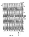
- Figure 5A is a plan view of a pattern layout illustrating the mask type Read Only Memory corresponding to the circuit of Figure 4;
- Figure 5B is a plan view of a pattern layout illustrating a portion of the mask type Read Only Memory cell of Figure 5A;
- Figure 5C is an equivalent circuit of the mask type Read Only Memory cell shown in Figure 5B;
- Figure 5D is a cross-sectional view taken along line II-II in Figure 5B; and
- Figures 6A to 6L are cross-sectional views of a semiconductor substrate -illustrating stages in a method of manufacturing a mask type Read Only Memory according to the preferred embodiment.
- An embodiment of a mask type Read Only Memory according to the preferred embodiment of the present invention will be described with reference to Figures 4, 5A, 5B, 5C and 5D of the drawings.
- Referring to Figure 4, the mask type Read Only Memory consists of a plurality of NAND gate blocks 100 arranged in a row and column matrix, each of the blocks is selectable by the output signals of a page,
decoder 44 and select signals sel0 to sel3. Each of the NAND gate blocks 100 includes fourNAND gate circuits A are applied. Predetermined data is permanently written intomatrix cell portions 200. - The Read Only Memory has a first and second power source terminals VDD2 and GND, an
output terminal 41, afirst branch node 42 and asecond branch node 43. A P-channel IGFET Q41 is connected between the first power source terminal VDD and theoutput terminal 41. An N-channel IGFET Q42 is connected between theoutput terminal 41 and thefirst branch node 42. Analuminium wiring electrode 45 interconnects thefirst branch node 42 and thesecond branch node 43. A first NAND gate circuit 46 and a secondNAND gate circuit 47 are connected between thebranch node 42 and GND. N-channel IGFETs Q43, Q44 in the first and secondNAND gate circuits 46, 47 select both of the first and secondNAND gate circuits 46, 47 simultaneously. N-channel IGFETs Q45, Q46 in the first andsecond NAND circuits 46, 47 select one ofNAND circuits 46 and 47. Thematrix cell portions 200 are connected to addressdecoder 48. - A
third NAND circuit 49 and afourth NAND circuit 50 are arranged in the same manner as first andsecond NAND circuits 46, 47. - Referring to Figures 5A to 5D, a polysilicon-gate electrode layer is formed by interposing an insulating
layer 71 between theP type substrate 61 and thegate electrode layer 69, and N+ diffusedregions regions regions aluminium wiring layer 80 is provided in the centre of the "8" shape diffused region, and thealuminium layer 80 connects with the diffusedregions contact holes regions channel regions 83. - A method of manufacturing a mask type Read Only Memory will be described referring to Figures 6A to 6L.
- A
thermal oxide film 62 of 1000A is formed over the entire surface of a P-type silicon substrate 61 which has been doped with boron by the thermal oxidation process. Asilicon nitride layer 63 of 30001 is deposited over the entire surface of the oxide film by the CVD process. Some areas of thesilicon nitride layer 63 on thesubstrate 61 where elements are to be formed, are removed by the photoengraving process (Figure 6A). A wet oxidation process is performed in order to form a thick Si02field oxide film 65 of 1 µm (Figure 6B). - As shown in Figure 6C, the remaining silicon nitride masks 64 and the
thermal oxide film 62 are removed by the engraving process. The surface of thesemiconductor substrate 61 is thus exposed. - A first thin insulating film (SiO2) 67 of 500 to 1000A thickness which serves as a gate oxide film, is formed on the exposed
surface 66 of thesemiconductor substrate 61. Next, apolysilicon layer 68 of 3000 to 4000A thickness is deposited over the entire surface by the CVD process (Figure 6D). - The
polysilicon layer 68 is subjected to a photoengraving process to form a given pattern, and thusgate electrodes gate electrodes gate oxide films PSG film 73 is deposited over the entire surface by the CVD process. Subsequently, by using thegate oxide films PSG film 73 is diffused into thesubstrate 61 to form N+-type drain andsource regions 74, 75 (Figure 6E). - The
PSG film 73 is then removed by etching. As shown in Figure 6F, an SiO2 film 78 of 2000 to 6000Å thickness is formed on the surface as a third insulating layer, by the CVD process.Contact hole 79 for analuminium wiring electrode 80 is formed in the Si02 film 78. Next, aluminium is vapour-deposited over the entire surface and is photo- etched to formbonding pads 81 andwiring electrodes 80 at given locations as shown in Figure 6G. Next, a photo-resistlayer 82 is formed over the surface to provide an etching mask, and the SiO2 film 78 covering the transistors which are to be of the depletion type in accordance with the information to be stored, is etched away. By using the Si02 film 78 (or resist 82) as a mask, impurity divalent phosphorus ions P++ of N type, with an energy of 160 KeV, are implanted into a channel region throughgate electrodes 69 and gate oxide film 71 (and theSiO 2 78A). An N type implantedchannel region 83 connecting the source and drain of the transistor is thus formed, and the transistor is rendered a depletion type (Figure 61). Next, as shown in Figure 6J, aprotective film 84 such as a BPSG (boron-doped phospho-silicate glass) film or PSG film or silicon nitride film, of 5000 to 7000A thickness is deposited over the surface by the plasma CVD method. The surfaceprotective film 84 is formed with concave regions corresponding to the depletion type transistors which represent the stored information. Accordingly, it is possible to check the stored information from the outer configuration of the device. Next, as shown in Figure 6K, abonding pad 81 for an outer-lead is exposed, and the chip fabricating process is completed. As shown in Figure 6L, an outer-lead 86 made from aluminium is connected to thebonding pad 81. - In the described method of making a mask type Read Only Memory, the ion implantation into the channel region to form a depletion type MOS transistor to determine the memory content of the device is performed at a late stage of the process. The fabrication process steps up to the deposition of the Si02 film following the formation of the MOS transistors may be performed in advance before the memory contents are determined. After the memory contents are determined in accordance with a customer's requirements, a mask for the memory contents is obtained, and the ion implantation into the above-mentioned channel regions and the remaining steps of the process are performed. Accordingly the period from when the memory contents are specified by a customer until the products storing those contents are completed is considerably reduced. Further, because the protective film covering each depletion type transistor in the memory region is concave in shape the contents stored may be checked externally.
Claims (5)
Applications Claiming Priority (2)
| Application Number | Priority Date | Filing Date | Title |
|---|---|---|---|
| JP56128450A JPS5830154A (en) | 1981-08-17 | 1981-08-17 | Fixed memory semiconductor device and manufacture thereof |
| JP128450/81 | 1981-08-17 |
Publications (4)
| Publication Number | Publication Date |
|---|---|
| EP0073130A2 true EP0073130A2 (en) | 1983-03-02 |
| EP0073130A3 EP0073130A3 (en) | 1985-01-16 |
| EP0073130B1 EP0073130B1 (en) | 1988-03-02 |
| EP0073130B2 EP0073130B2 (en) | 1993-05-12 |
Family
ID=14985006
Family Applications (1)
| Application Number | Title | Priority Date | Filing Date |
|---|---|---|---|
| EP82304312A Expired - Lifetime EP0073130B2 (en) | 1981-08-17 | 1982-08-16 | Method for manufacturing a mask type read only memory |
Country Status (4)
| Country | Link |
|---|---|
| US (1) | US4467520A (en) |
| EP (1) | EP0073130B2 (en) |
| JP (1) | JPS5830154A (en) |
| DE (1) | DE3278182D1 (en) |
Cited By (10)
| Publication number | Priority date | Publication date | Assignee | Title |
|---|---|---|---|---|
| EP0132033B1 (en) * | 1983-07-19 | 1988-03-02 | American Microsystems, Incorporated | Process of producing custom programmed read only memory |
| EP0450389A2 (en) * | 1990-03-30 | 1991-10-09 | STMicroelectronics S.r.l. | A low-capacitance, high breakdown voltage programmed cell structure for read-only memory circuits |
| US5081052A (en) * | 1986-06-25 | 1992-01-14 | Hitachi, Ltd. | ROM and process for producing the same |
| FR2670316A1 (en) * | 1990-12-10 | 1992-06-12 | Samsung Electronics Co Ltd | Process for manufacturing a masked read-only memory device |
| US5219776A (en) * | 1990-07-30 | 1993-06-15 | Sharp Kabushiki Kaisha | Method of manufacturing semiconductor device |
| US5278078A (en) * | 1991-05-14 | 1994-01-11 | Kabushiki Kaisha Toshiba | Method of manufacturing semiconductor device |
| US5350703A (en) * | 1992-08-20 | 1994-09-27 | Gold Star Electron Co., Ltd. | Method for fabrication mask ROM |
| US5486487A (en) * | 1990-03-30 | 1996-01-23 | Sgs-Thomson Microelectronics S.R.L. | Method for adjusting the threshold of a read-only memory to achieve low capacitance and high breakdown voltage |
| US5975647A (en) * | 1996-12-20 | 1999-11-02 | Skf Industrie S. P. A. | Wheel hub unit |
| US6076896A (en) * | 1996-10-01 | 2000-06-20 | Skf Industrie S.P.A. | Wheel hub or hub unit allowing improved mounting and removal of a brake member |
Families Citing this family (19)
| Publication number | Priority date | Publication date | Assignee | Title |
|---|---|---|---|---|
| US4536944A (en) * | 1982-12-29 | 1985-08-27 | International Business Machines Corporation | Method of making ROM/PLA semiconductor device by late stage personalization |
| JPS60174682A (en) * | 1984-02-20 | 1985-09-07 | Tsukahara Kogyo Kk | Production of elastic porous stamp material |
| JPS61287164A (en) * | 1985-06-13 | 1986-12-17 | Ricoh Co Ltd | Semiconductor memory device |
| JPH06104358B2 (en) * | 1985-06-24 | 1994-12-21 | 塚原工業株式会社 | Method for manufacturing ink occlusion type stamp material |
| JPS6292362A (en) * | 1985-10-17 | 1987-04-27 | Toshiba Corp | Manufacture of semiconductor device |
| JPS6381948A (en) * | 1986-09-26 | 1988-04-12 | Toshiba Corp | Multilayer interconnection semiconductor device |
| US5019878A (en) * | 1989-03-31 | 1991-05-28 | Texas Instruments Incorporated | Programmable interconnect or cell using silicided MOS transistors |
| US5068696A (en) * | 1989-03-31 | 1991-11-26 | Texas Instruments Incorporated | Programmable interconnect or cell using silicided MOS transistors |
| US5091328A (en) * | 1989-11-21 | 1992-02-25 | National Semiconductor Corporation | Method of late programming MOS devices |
| US5432103A (en) * | 1992-06-22 | 1995-07-11 | National Semiconductor Corporation | Method of making semiconductor ROM cell programmed using source mask |
| JP3177036B2 (en) * | 1992-12-24 | 2001-06-18 | 三菱鉛筆株式会社 | Method for producing sponge rubber print having open cells |
| US5592012A (en) * | 1993-04-06 | 1997-01-07 | Sharp Kabushiki Kaisha | Multivalued semiconductor read only storage device and method of driving the device and method of manufacturing the device |
| US5429974A (en) * | 1993-10-22 | 1995-07-04 | United Microelectronics Corporation | Post passivation mask ROM programming method |
| US5514609A (en) * | 1994-05-13 | 1996-05-07 | Mosel Vitelic, Inc. | Through glass ROM code implant to reduce product delivering time |
| US5796149A (en) * | 1994-09-09 | 1998-08-18 | Nippon Steel Corporation | Semiconductor memory using different concentration impurity diffused layers |
| US5514610A (en) * | 1995-03-17 | 1996-05-07 | Taiwan Semiconductor Manufacturing Company | Method of making an optimized code ion implantation procedure for read only memory devices |
| GB2300983A (en) * | 1995-05-13 | 1996-11-20 | Holtek Microelectronics Inc | Flexible CMOS IC layout method |
| US5693551A (en) * | 1995-09-19 | 1997-12-02 | United Microelectronics, Corporation | Method for fabricating a tri-state read-only memory device |
| US6238983B1 (en) * | 1999-08-30 | 2001-05-29 | Taiwan Semiconductor Manufacturing Company | Alignment dip back oxide and code implant through poly to approach the depletion mode device character |
Citations (4)
| Publication number | Priority date | Publication date | Assignee | Title |
|---|---|---|---|---|
| US3914855A (en) * | 1974-05-09 | 1975-10-28 | Bell Telephone Labor Inc | Methods for making MOS read-only memories |
| US4129936A (en) * | 1976-09-09 | 1978-12-19 | Sakae Takei | Method for manufacturing monolithic semiconductor mask programmable ROM's |
| GB2017406A (en) * | 1978-03-20 | 1979-10-03 | Texas Instruments Inc | Implant programmable semi- conductor read only memory |
| US4235010A (en) * | 1975-09-04 | 1980-11-25 | Hitachi, Ltd. | Semiconductor integrated circuit device composed of insulated gate field-effect transistor |
Family Cites Families (10)
| Publication number | Priority date | Publication date | Assignee | Title |
|---|---|---|---|---|
| JPS5375781U (en) * | 1976-11-29 | 1978-06-24 | ||
| US4108686A (en) * | 1977-07-22 | 1978-08-22 | Rca Corp. | Method of making an insulated gate field effect transistor by implanted double counterdoping |
| US4384399A (en) * | 1978-03-20 | 1983-05-24 | Texas Instruments Incorporated | Method of making a metal programmable MOS read only memory device |
| US4364167A (en) * | 1979-11-28 | 1982-12-21 | General Motors Corporation | Programming an IGFET read-only-memory |
| US4336647A (en) * | 1979-12-21 | 1982-06-29 | Texas Instruments Incorporated | Method of making implant programmable N-channel read only memory |
| US4356042A (en) * | 1980-11-07 | 1982-10-26 | Mostek Corporation | Method for fabricating a semiconductor read only memory |
| US4406049A (en) * | 1980-12-11 | 1983-09-27 | Rockwell International Corporation | Very high density cells comprising a ROM and method of manufacturing same |
| US4380866A (en) * | 1981-05-04 | 1983-04-26 | Motorola, Inc. | Method of programming ROM by offset masking of selected gates |
| US4364165A (en) * | 1981-05-28 | 1982-12-21 | General Motors Corporation | Late programming using a silicon nitride interlayer |
| US4365405A (en) * | 1981-05-28 | 1982-12-28 | General Motors Corporation | Method of late programming read only memory devices |
-
1981
- 1981-08-17 JP JP56128450A patent/JPS5830154A/en active Granted
-
1982
- 1982-08-16 DE DE8282304312T patent/DE3278182D1/en not_active Expired
- 1982-08-16 EP EP82304312A patent/EP0073130B2/en not_active Expired - Lifetime
- 1982-08-17 US US06/408,873 patent/US4467520A/en not_active Expired - Lifetime
Patent Citations (4)
| Publication number | Priority date | Publication date | Assignee | Title |
|---|---|---|---|---|
| US3914855A (en) * | 1974-05-09 | 1975-10-28 | Bell Telephone Labor Inc | Methods for making MOS read-only memories |
| US4235010A (en) * | 1975-09-04 | 1980-11-25 | Hitachi, Ltd. | Semiconductor integrated circuit device composed of insulated gate field-effect transistor |
| US4129936A (en) * | 1976-09-09 | 1978-12-19 | Sakae Takei | Method for manufacturing monolithic semiconductor mask programmable ROM's |
| GB2017406A (en) * | 1978-03-20 | 1979-10-03 | Texas Instruments Inc | Implant programmable semi- conductor read only memory |
Cited By (11)
| Publication number | Priority date | Publication date | Assignee | Title |
|---|---|---|---|---|
| EP0132033B1 (en) * | 1983-07-19 | 1988-03-02 | American Microsystems, Incorporated | Process of producing custom programmed read only memory |
| US5081052A (en) * | 1986-06-25 | 1992-01-14 | Hitachi, Ltd. | ROM and process for producing the same |
| EP0450389A2 (en) * | 1990-03-30 | 1991-10-09 | STMicroelectronics S.r.l. | A low-capacitance, high breakdown voltage programmed cell structure for read-only memory circuits |
| EP0450389A3 (en) * | 1990-03-30 | 1994-02-23 | Sgs Thomson Microelectronics | |
| US5486487A (en) * | 1990-03-30 | 1996-01-23 | Sgs-Thomson Microelectronics S.R.L. | Method for adjusting the threshold of a read-only memory to achieve low capacitance and high breakdown voltage |
| US5219776A (en) * | 1990-07-30 | 1993-06-15 | Sharp Kabushiki Kaisha | Method of manufacturing semiconductor device |
| FR2670316A1 (en) * | 1990-12-10 | 1992-06-12 | Samsung Electronics Co Ltd | Process for manufacturing a masked read-only memory device |
| US5278078A (en) * | 1991-05-14 | 1994-01-11 | Kabushiki Kaisha Toshiba | Method of manufacturing semiconductor device |
| US5350703A (en) * | 1992-08-20 | 1994-09-27 | Gold Star Electron Co., Ltd. | Method for fabrication mask ROM |
| US6076896A (en) * | 1996-10-01 | 2000-06-20 | Skf Industrie S.P.A. | Wheel hub or hub unit allowing improved mounting and removal of a brake member |
| US5975647A (en) * | 1996-12-20 | 1999-11-02 | Skf Industrie S. P. A. | Wheel hub unit |
Also Published As
| Publication number | Publication date |
|---|---|
| EP0073130B1 (en) | 1988-03-02 |
| EP0073130A3 (en) | 1985-01-16 |
| EP0073130B2 (en) | 1993-05-12 |
| DE3278182D1 (en) | 1988-04-07 |
| JPH0328832B2 (en) | 1991-04-22 |
| JPS5830154A (en) | 1983-02-22 |
| US4467520A (en) | 1984-08-28 |
Similar Documents
| Publication | Publication Date | Title |
|---|---|---|
| EP0073130B1 (en) | Method for manufacturing a mask type read only memory | |
| US5389558A (en) | Method of making a semiconductor memory circuit device | |
| US4080718A (en) | Method of modifying electrical characteristics of MOS devices using ion implantation | |
| US4755864A (en) | Semiconductor read only memory device with selectively present mask layer | |
| US4367580A (en) | Process for making polysilicon resistors | |
| US5517061A (en) | CMOS read only memory with programming at the second metal layer on a two-metal process | |
| US5063170A (en) | Semiconductor integrated circuit device and a method of producing the same | |
| US7339220B2 (en) | Memory device with surface-channel peripheral transistors | |
| US4151020A (en) | High density N-channel silicon gate read only memory | |
| US4219836A (en) | Contact programmable double level polysilicon MOS read only memory | |
| US4525809A (en) | Integrated circuit | |
| US4608748A (en) | Method of manufacturing a memory FET with shorted source and drain region | |
| US5149667A (en) | Mask ROM device having double polycrystalline silicone and process for producing the same | |
| US4271421A (en) | High density N-channel silicon gate read only memory | |
| US4342100A (en) | Implant programmable metal gate MOS read only memory | |
| KR100251229B1 (en) | Advanced nor type read only memory and fabricating method thereof | |
| US6150198A (en) | Method of fabricating semiconductor read-only memory device with reduced parastic capacitance between bit line and word line | |
| US4208726A (en) | Programming of semiconductor read only memory | |
| US6436772B2 (en) | Method of manufacturing semiconductor device having memory cell transistors | |
| US6353243B1 (en) | Process for manufacturing an integrated circuit comprising an array of memory cells | |
| EP0447976A1 (en) | Read-only semiconductor memory device | |
| US5949704A (en) | Stacked read-only memory | |
| US5911107A (en) | MOS transistor read-only memory device | |
| JP2834179B2 (en) | Method for manufacturing semiconductor integrated circuit device | |
| KR0165469B1 (en) | Mask rom & method of manufacture thereof |
Legal Events
| Date | Code | Title | Description |
|---|---|---|---|
| PUAI | Public reference made under article 153(3) epc to a published international application that has entered the european phase |
Free format text: ORIGINAL CODE: 0009012 |
|
| AK | Designated contracting states |
Designated state(s): DE FR GB |
|
| RAP1 | Party data changed (applicant data changed or rights of an application transferred) |
Owner name: KABUSHIKI KAISHA TOSHIBA |
|
| PUAL | Search report despatched |
Free format text: ORIGINAL CODE: 0009013 |
|
| RHK1 | Main classification (correction) |
Ipc: H01L 29/82 |
|
| AK | Designated contracting states |
Designated state(s): DE FR GB |
|
| 17P | Request for examination filed |
Effective date: 19850621 |
|
| 17Q | First examination report despatched |
Effective date: 19860404 |
|
| GRAA | (expected) grant |
Free format text: ORIGINAL CODE: 0009210 |
|
| AK | Designated contracting states |
Kind code of ref document: B1 Designated state(s): DE FR GB |
|
| REF | Corresponds to: |
Ref document number: 3278182 Country of ref document: DE Date of ref document: 19880407 |
|
| ET | Fr: translation filed | ||
| PLBI | Opposition filed |
Free format text: ORIGINAL CODE: 0009260 |
|
| 26 | Opposition filed |
Opponent name: DEUTSCHE ITT INDUSTRIES GMBH, FREIBURG Effective date: 19881201 |
|
| ET1 | Fr: translation filed ** revision of the translation of the patent or the claims | ||
| PUAH | Patent maintained in amended form |
Free format text: ORIGINAL CODE: 0009272 |
|
| STAA | Information on the status of an ep patent application or granted ep patent |
Free format text: STATUS: PATENT MAINTAINED AS AMENDED |
|
| 27A | Patent maintained in amended form |
Effective date: 19930512 |
|
| AK | Designated contracting states |
Kind code of ref document: B2 Designated state(s): DE FR GB |
|
| ET | Fr: translation filed |
Free format text: BO 12/93 PAGE 167: ANNULATION |
|
| ET3 | Fr: translation filed ** decision concerning opposition | ||
| PGFP | Annual fee paid to national office [announced via postgrant information from national office to epo] |
Ref country code: GB Payment date: 19970807 Year of fee payment: 16 |
|
| PGFP | Annual fee paid to national office [announced via postgrant information from national office to epo] |
Ref country code: FR Payment date: 19970811 Year of fee payment: 16 |
|
| PGFP | Annual fee paid to national office [announced via postgrant information from national office to epo] |
Ref country code: DE Payment date: 19970822 Year of fee payment: 16 |
|
| PG25 | Lapsed in a contracting state [announced via postgrant information from national office to epo] |
Ref country code: GB Free format text: LAPSE BECAUSE OF NON-PAYMENT OF DUE FEES Effective date: 19980816 |
|
| GBPC | Gb: european patent ceased through non-payment of renewal fee |
Effective date: 19980816 |
|
| PG25 | Lapsed in a contracting state [announced via postgrant information from national office to epo] |
Ref country code: FR Free format text: LAPSE BECAUSE OF NON-PAYMENT OF DUE FEES Effective date: 19990430 |
|
| PG25 | Lapsed in a contracting state [announced via postgrant information from national office to epo] |
Ref country code: DE Free format text: LAPSE BECAUSE OF NON-PAYMENT OF DUE FEES Effective date: 19990601 |
|
| REG | Reference to a national code |
Ref country code: FR Ref legal event code: ST |
|
| APAH | Appeal reference modified |
Free format text: ORIGINAL CODE: EPIDOSCREFNO |