EP0073078A2 - Modular switching network for telecommunication system - Google Patents
Modular switching network for telecommunication system Download PDFInfo
- Publication number
- EP0073078A2 EP0073078A2 EP82200992A EP82200992A EP0073078A2 EP 0073078 A2 EP0073078 A2 EP 0073078A2 EP 82200992 A EP82200992 A EP 82200992A EP 82200992 A EP82200992 A EP 82200992A EP 0073078 A2 EP0073078 A2 EP 0073078A2
- Authority
- EP
- European Patent Office
- Prior art keywords
- control unit
- interfaces
- data words
- peripheral units
- register
- Prior art date
- Legal status (The legal status is an assumption and is not a legal conclusion. Google has not performed a legal analysis and makes no representation as to the accuracy of the status listed.)
- Granted
Links
Images


Classifications
-
- H—ELECTRICITY
- H04—ELECTRIC COMMUNICATION TECHNIQUE
- H04Q—SELECTING
- H04Q11/00—Selecting arrangements for multiplex systems
- H04Q11/04—Selecting arrangements for multiplex systems for time-division multiplexing
Landscapes
- Engineering & Computer Science (AREA)
- Computer Networks & Wireless Communication (AREA)
- Use Of Switch Circuits For Exchanges And Methods Of Control Of Multiplex Exchanges (AREA)
- Data Exchanges In Wide-Area Networks (AREA)
Abstract
Description
- The present invention relates to a switching network adapted to facilitate selective message transmission among a multiplicity of peripheral units, such as subscriber stations or trunk lines, with the aid of signal-routing modules serving as automatic exchanges in a telecommunication system.
- In such automatic exchanges it is known to provide routing modules, e.g. in the form of orthogonal switching matrices, responsive to instructions from associated control units which in turn may be commanded by a central controller. As a given switching matrix serves only a limited number of peripheral units, the several matrices must be able to intercommunicate in order to establish signal paths between stations respectively served thereby. This creates problems when the network must be expanded to accomodate additional subscribers and/or to provide for a greater variety of available services.
- The object of present invention, therefore, is to provide a network of this type which has the flexibility and adaptability required for expansion and/or service modification in a relatively simple and economical manner.
- In accordance with present invention, each of several signal-routing modules of a switching network for a telecommunication system has a set of input/output terminals connected to respective peripheral units of a group individually associated therewith. Each module comprises a control unit as well as a plurality of interfaces which are each connected, via corresponding subsets of the set of terminals, to a plurality of peripheral units in a respect-Lve subgroup of the associated group. Each module also comprises first register means connected to the output of said interfaces, each of these first register means comprising a number of registers corresponding to the number of subgroup units associated to each of said interfaces, each register being enabled by timing signals from control unit to load digital data words of a channel coming from a correspondent peripheral unit. A first channel concentrator in each module has input connections to said first register means and has a reduced number of outputs carrying in each phase the bits of an incoming data word selectively extracted therefrom on instructions from the control unit. A second channel concentrator in each module has input connections to second register means provided for , temporarily storing data words coming from the outputs of said first channel concentrator of each module and has a reduced number of outputs carrying in each phase the bits of an outgoing data word extracted therefrom also in response to instructions from the control unit.
- Pursuant to a more particular feature of the invention, the distribution means may comprise a channel expander (roughly complementary to the first channel concentrator) and a plurality of data stores in which the expander enters outgoing data words destined for any of the interfaces of the module concerned.
- According to a preferred embodiment of the invention each interface includes third register means (one for each of the k peripheral units) for temporarily storing incoming data words of m bits each (m being preferably equal to 8, in conformity with the usual practice) which represent message samples of PCM channels received from the associated subgroup of peripheral units in respective time slots of an operating cycle; such a cycle coincides with a recurrent PCM frame which is divided into a multiplicity of phases, each time slot encompassing k phases.
- According to a preferred embodiment of the invention, each interface further includes fourth register means for temporarily storing outgoing data words destined for the peripheral units in the associated subgroup, these outgoing data words being selectively fed thereto by distributing means inserted between the second channel concentrator and the several interfaces. The feeding of the outgoing data words to the fourth register means and thence to designated peripheral units of the associated subgroup takes place under instructions from the control unit delivered to the distributing means and to the fourth register means.
- In the network particularly described hereinafter, each peripheral unit is linked with an interface terminal of the associated module through a bidirectional connection (e.g. a telephone line or a trunk). In principle, however, the invention is also applicable to systems in which incoming data words are received only from peripheral units acting as sources while outgoing data words are sent to other peripheral units acting as loads.
- Advantageously, the number of peripheral units served by each interface of a routing module does not exceed the number of phases in a PCM frame; with the usual number of 32 time slots per frame, the maximum number of peripheral units in each subgroup is thus 256. This will insure that under certain operating conditions, when all the peripheral units associated with a single interface of a module are active while the others are not, the data words or bytes received from all these active peripheral units will pass at least the first channel concentrator.
- In the specific embodiment here disclosed, each module has eight interfaces accomodating up to 2,048 peripheral units. With the first concentrator of each routing module handling a maximum of 256 PCM channels, this allows for the establishment of simultaneous signal paths between up to 25% of all peripheral units served by the network, provided they are well distributed among the groups associated with the several modules. If necessary, of course, the maximum ration of the number of simultaneous active peripheral units to the total number thereof can be increased by doubling or otherwise enlarging the output capacity of the two channel concentrators of one or more modules.
- In a telephone system or the like, the control unit of any module will generally emit routing instructions on the basis of call signals received from an associated station and conveyed to the control unit of a module serving a called station (if the two modules are different) via the intermodule connection available for the transmission of data words. In some systems, however, these control units could also be connected by a centralized higher-ranking controller to establish and terminate connections between specified peripheral units, e.g. in accordance with a predetermined program.
- The above and other features of the present invention will now be described in detail with reference to the accompanying drawing in which:
- FIG. 1 is a block diagram of a switching network according to the present invention including a plurality of structurally identical routing modules;
- FIG. 2 is a block diagram of one of the routing modules of FIG. 1, showing several structurally identical input/output interfaces;
- FIG. 3 is a block diagram of a first part of an interface of FIG. 2, designed for the handling of incoming data words;
- FIG. 4 is a block diagram of a second part of the interface illustrated in FIGS. 2 and 3, designed for the handling of outgoing data words;
- FIGS. 5A and 5B are two time diagrams relating to the processing of incoming data words by the interface components illustrated in FIG. 3; and
- FIG. 5C is a time diagram relating to the processing of outgoing data words by the interface components illustrated in FIG. 4.
- As illustrated in FIG. 1, a switching network according to the present invention comprises a plurality of signal-
routing modules Module 12a is connected tomodules 12b, 12c ...12f via respectivebidirectional signal paths Module 12b is directly linked tomodules bidirectional paths modules paths Similar transmission paths modules module 12d whilemodules bidirectional path 46 with each other. - Thus, each module in the telecommunication system of FIG. 1 exchanges information with all the other modules of the network.
- Each
module respective feedback loop feedback loops - Each module of FIG. 1 is further tied via a number of
bidirectional multiples 60 to a respective group of associatedperipheral units multiples 60 is assumed to be in analog form though this need not be the case. The full-mesh interconnection ofswitching modules units 52a-52f indicates that they act as the input/output parts of the overall system. - The modular design of a switching network according to the present invention facilitates the addition of peripheral units that are geographically remote from the pre-existing peripheral units thereof. Any such remote peripheral units can be connected to the network through an additional routing module in turn tied to each of the exisiting modules via a respective bidirectional communication path.
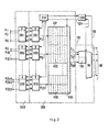
- As particularly illustrated in FIG. 2 for
routing module 12a, each modules includes eight interfaces 151-158 with up to 256 terminals a1 - a256 connected at least in part to respective peripheral units. These interfaces have input multiples 64 (only two shown) extending to respective data stores 161-168. Each of these data stores comprises 256 pairs of 20-bit registers, the registers of each pair being alternately enabled by timing signals from acontrol unit 120 to load 20-bit data words carried in corresponding phases of consecutive recurrences of an incoming PCM frame. - Data stores 161-168 are linked to a channel concentrator or compressor 66 (essentially a PCM multiplexer) which, in response to instructions received from
control unit 120 via abus 124, selectively reads out the contents of their registers onto a 20-lead output multiple 68. This multiple extends to a plurality of transmittingjunctors routing module Feedback loop 50a serves as an output multiple ofjunctor 74a whereasjunctors 74b-74f have output multiples 16', 18', 20', 22', 24' respectively included in thebidirectional signal paths buses 128 to controlunit 120 for receiving therefrom instructions to be transmitted to all the modules of the network. The control unit also communicates with interfaces 151-158 by way of abidirectional bus 122. -
Module 12a further incorporates a plurality of receivingjunctors modules 12a-12f. Junctor 80a is connected to transmittingjunctor 74a viafeedback loop 50a whereasjunctors 80b-80f receive signals from modules 13D -12f viamultiples 16", 18", 20", 22" and 24" also included inbidirectional signal paths junctors 80a-80f haverespective output multiples data stores 81a-81f each advantageously comprising 257 pairs of registers, the registers of 256 of these pairs each having 20 stages for the memorization of 20-bit data words arriving from the several modules overfeedback loop 50a and bidirection-L alpaths junctors 80a-80f, ( the remaining 257th pair of registers being destined to store, as described hereinafter, the instruction bits coming from control unit 120 ). -
Data stores 81a-81f are connected to achannel concentrator 90 also designed as a PCM multiplexer. In response to commands fromunit 120,concentrator 90 selectively transmits onto a 20-lead multiple 92 data words written in the registers ofstores 81a-81f. During each frame period, i.e. during a time interval coinciding with the transmission of an incoming PCM frame byconcentrator 66 or with the reception of an outgoing PCM frame by anyjunctor 80a-80f,concentrator 90 selects 256 data words from among the 6 x 257 words registered instores 81a-81f and emits the selected words in successive phases of an outgoing frame. The selected data words are conveyed to a channel expander 98 (essentially a PCM demultiplexer) via multiple 92 and to aconference bridge 110 via abranch 112 of that multiple. As described in greater detail hereinafter,conference bridge 110 facilitates multiparty telephone calls among subscriber stations represented by the peripheral units of FIG. 1;bridge 110 transmits output signals to expander 98 via a data multiple 114 in response to instructions received fromcontrol unit 120 on acommand bus 144. A two-way connection 145 links theunit 120 with a central controller (not shown) for the performance of ancillary operations such as data storage, error detection and man/ machine dialoguing. -
Channel expander 98 is connected on its output side to eight data stores 17-178 which have output multiples 100 (only two shown in FIG. 2) extending to respective interfaces 151-158. In accordance with switching commands received fromcontrol unit 120 via abus 146, expander 98 loads signals arriving overmultiples expander 98 in accordance with the commands fromcontrol unit 120 are loaded with data words during any given frame period while corresponding registers of nonselected pairs do not receive any data. During the succeeding frame period the previously loaded registers of each selected data store 171-178 are enabled in a pre-established sequence to read their contents onto the associated output multiple 100, as described in detail hereinafter with reference to FIG. 5C. - As illustrated in FIGS. 3 and 4, interface 151 - which is structurally identical with interfaces 152-158 - comprises a
first section 200 connected to 256 peripheral units out of an assumed total of 2,048 such units associated with module 17a. Asecond section 300 ofinterface 151 is disposed betweensection 200 and the other components ofmodule 12a, particularly the associateddata stores Section 200 includes 32 input/output ports 201-232 each tied to eight peripheral units of the associated subgroup. Ports 201-232 comprise hybrid circuits for performing the conversion of each outer route allocated to a peripheral unit into two routes respectively allocated to the transmission and the reception side of the module. - Each port 201-232 is provided with a sensing circuit x which scans the associated subscriber lines for detecting a signal indicating an attempt to establish a calling connection; this information is transmitted to control
unit 120 which responds thereto as described hereinafter. Where the peripheral units 52 are conventional telephones, such a signal indicates an off-hook condition of a telephone handset. The release of a line is similarly reported to the control unit. -
Section 300 includes 32 sets of eight transcoders 301-332 respectively connected to the input/output ports 201-232 for digitizing incoming analog signals (e.g. voice samples) and for converting into analog form digital signals outcoming frombuffer component 500 of FIG. 4. Ports 201-232 may be adapted to transform incoming analog voltages into waveforms having voltage levels suitable for digitization by the analog-to-digital converters of these transcoders. - The transcoders 301-332 may incorporate signal generators which emit ringing signals to called peripheral units and ringing, dial or busy tones to calling peripheral units by way of the hybrid circuits of ports 201-232, the signal generators being activated in response to commands transmitted from
control unit 120 over abuffer circuit 333 and logic circuits Y included in the transcoders. Alternatively, the signal generators may be included in these hybrid circuits and activated by the sensing circuits x which are coupled to the respective logic circuits y. - In response to commands from
control unit 120, each logic circuit y controls the respective set of eight transcoders for analog/ digital conversion of signals arriving from the eight associated peripheral units via the intervening group of eight input/output ports. The bits of incoming data words (bytes) serially emitted on transcoder outputs el-e32 are fed to respective pairs 401-432 of 8-bit registers. - As illustrated in rows el-e32 of FIG. 5A, data words (labeled 1-256 according to their originating terminals a1-a256) are transmitted from transcoder circuits 301-332 to register pairs 401-432 in a 125-microsecond operating cycle (corresponding to a PCM frame) subdivided into eight subcycles each having a duration of 15.625 microseconds. Each transcoder emits one 8-bit word or byte during each subcycle. However, the emission times are staggered so that eight preselected transcoders of
sets sets further transcoders 303, 307, etc. utilize a third time slot and the remaining eighttranscoders 304, 308, etc. are active during a fourth time slot; each time slot is approximately 3.096 microseconds in duration. - As further illustrated in FIG. 3, register pairs 401-432 are connected to a series-to-
parallel converter 433 which transmits todata 161 during each time slot of an operating cycle the information received by eight of these registers during the immediatly preceding time slot.Converter 433 is also designed to append a 12-bit error-correction code to the bytes arriving from transcoders 301-332 via register pairs 401-432. The resulting 20 bits of each data word are emitted over respective leads fl-f20 todata store 161. The order in which the information is transmitted is controlled byunit 120 viabus 124.. - As indicated in graphs e and f of FIG. 5B, each of the 32 time slots of an operating cycle of
interface 151 is divided into eight phases during each of which a data word - labeled in graph e as in FIG. 5A - is transmitted in parallel form to a respective register indata store 161 from an associated register in group 401-432. During phases 9-16 corresponding to the second time slot of an operating cycle, graph f, series-to-parallel converter 433 transmits from register pairs 401, 405, 409, 413, 417, 421, 425, 429 the bytes loaded into one register of each pair during the first time slot of the cycle. The first bytes fed by loads e2, e6, e10, e14, e18, e22, e26, e30 into the data receiving registers ofpairs 402, 406, 410, 414, 418, 422, 426, 430 during the second time slot of the first subcycle, as partly illustrated in FIG. 5B, are transferred byconverter 433 todata store 161 during the series of phases 17-24 coinciding with the third time slot of that subcycle. Thus, the eight registers of group 401-432 receiving byte sequences from transcoders 301-332 in one time slot of an operating cycle are read out toconverter 433 in the succeeding time slot. - During the common operating cycle of interfaces 151-158, data stores 161-168 can each receive 256 incoming 20-bit words for temporary memorization by registers thereof activated for reception by
control unit 120 which includes a nonillustrated time base. Each of these momentarily data-receiving registers is paired with a respective structurally identical 20-bit register which was activated during the preceding operating cycle for receiving a data group from therespective converter 433 in the associated interface. During any such operating cycle, the 20 bits of each data word written in each of the 2,048 registers of data stores 161-168 activated for writing during the preceding cycle are selectively unloaded in parallel onto multiple 68 in response to reading commands received fromcontrol unit 120 viabus 124. Not more than 256 words, however, may be emitted byconcentrator 66 in a PCM frame outgoing over multiple 68; that frame thus includes 256 channels and is contemporaneous with an operating cycle of interfaces 151-158 and data stores 161-168. - As also illustrated in FIG. 3,
control unit 120 is provided with anoutput connection 69 which may be formed as part of bus 128 (FIG. 2). This connection carries instructions regarding the establishment and release of signal paths between pairs of peripheral units 52 (FIG. 1), or among a larger number of peripheral units in the case of conference calls. Theoutput multiples 50a, 16', 18', 20', 22', 24' of transmitting junctors 74a-74f (sse FIG. 2) must therefore each include 20 leads branched off multiple 68 and one or more further leads extending fromconnection 69; the same number of leads are, of course, required for the input multiples of receiving junctors 80a-80f. Moreover,data stores 81a-81f have 257 register pairs each, i.e. 256 register pairs for temporarily memorizing outgoing data words to be emitted on multiple 92 and an additional register pair for storing instruction bits generated by thecontrol unit 120 of arespective module 12a-12f. As shown in FIG. 2,concentrator 90 is provided with anoutput connection 141 extending to controlunit 120 for supplying same with instructions words from all six modules in as amny supervisory channels addressed by switching commands fed to multiplexer 90 bycontrol unit 120 via abus 142. - As shown in FIG. 4, each interface 151-158 incorporates in section 300 a
buffer component 500 including a parallel-to-series converter 509 inserted between the 20-lead multiple 100, extending fromdata store 171, and eight pairs 501-508 of 8-stage registers. Register pairs 501-508 are connected via respective output leads 511-518 to respective groups of four sets of transcoders in the associated set 301-332. -
Data store 171 shown in FIG. 4 contains 256 pairs of 20-stage registers, each such pair being assigned to a respective input/ output terminal a1-a256 of the hybrid circuits forming part of ports 201-232; obviously, some of these terminals may not be connected to peripheral units. Upon saturation of the network, further modules may be readily added to increase its capacity, e.g. up to 16. - During an operating cycle of
routing module 12a, up to 256 outgoing 20-bit data words are extracted by concentrator 90 from selected read-enabled registers ofstores 81a-81f and are distri- buted byexpander 98 to respective registers in stores 171-178 in accordance with commands fromcontrol unit 120. Whileexpander 98 is loading the write enabled registers ofstore 171 with data bits to be sent out, that store delivers to 20-lead multiple 100 the contents of registers which were activated to receive data during the preceding operating cycle but which are enabled to emit data during the current cycle. - Data emission from the read-enabled registers of
store 171 to terminals al-a256 ofinterface 151 proceeds according to graphs a and t of FIG. 5C. An operating cycle of 125 microseconds, corresponding to a PCM frame, is divided into 32 time slots each consisiting of eight phases illustrated in graph t. During each time slot,buffer component 500 receives eight 20-bit data words destined for respective transcoder groups 301-304, ...329-332. Parallel-to-series converter 309 transforms each arriving 20-bit word into an -bit word while simultaneously executing any corrections indicated by the 12-bit error code included in the arriving word. The resulting byte is loaded byconverter 509 into a data-receiving register of a pair selected in accordance with the temporal position of the word in an operating cycle, i.e. in accordance with the phase in which the 20-bit word arrived over multiple 100. - As shown in graph a of FIG. 5C, data words arriving in phases Nos. 1-8 constituting the first time slot of an operating cycle are to be ultimately transmitted to peripheral units connected to ter- minals a1, a33, a97, a 129, a161, al93, a225, respectively, or
interface section 200. During this first time slot the outgoing bytes are loaded in 8-bit form into write-activated registers of respective pairs 501-508. During the next time slot the bits of each byte are serially emitted onto leads 511-518 from register pairs 501-508. The byte destined for the peripheral unit connected to terminal a1 ofinterface section 201 is transmitted vialead 511 to all the digital/analog converters in transcoders 301-304;control unit 120, however, activates only the corresponding converter of transcoder set 301 viabuffer circuit 333 and the logic circuit y of that transcoder. Analogous routing procedures are used for the bytes emitted onto leads 512-518 from the read-enabled registers of pairs 502-508. - During phases Nos. 9-16 of an operating cycle, i.e. in the course of its second time slot, write-activated registers of pairs 501-508 are fed bytes carrying information ultimately destined for peripheral units connected to terminals a2, a34, a66, a98, a130, a162, a194, a226 of
interface section 200. In the 9th phase, even as a 20-nit data word intended for terminal a? is received in parallel form byconverter 509, read-enabled registers of pairs 501-508 emit onto leads 511-518 the first bits of the bytes received during phases Nos. 1-8, respectively. The 2nd through 8th bits of these previously received bytes are emitted in the phases Nos. 10 through 16, respectively. Thus, the bits of data words consecutively transmirted in parallel over multiple 100 in the eight phases of a time slot and transformed into bytes forconverter 509 are successively loaded into respective write-activated registers of pairs 501-508, being then concurrently read out in series over respective output leads 511-518 during the succeeding time slot. Data emission from the read-enabled registers of pairs 501-508 is carried out in response to commands generated bycontrol unit 120 on a connection 122' forming part of bus 122 (see FIG. 2). - Upon defecting an off-hook condition (seizure) in a line connected to an input/output terminal, the sensing circuit x of the respective port 201-208 emits an identification signal toward
control unit 120 through the logic circuit y of the associated transcoders and viabuffer circuit 333, this identification signal coding the the identity of the calling subscriber station. - In response to the identification signal, the control unit assigns to the calling station a first channel in the PCM frame carried by multiple 68 (FIG. 2) and a second channel in the PCM frame carried by multiple 92, these channels corresponding to respective phases in the operating cycle of switching
module 12a.Control unit 120 then enables the emission of a dial tone to the calling station. Preferably, the dial tone is generated by a circuit incorporated inexpander 98 and is selectively transmittable to all the transcoders in interfaces 151-158 in response to commands generated by control unit onbus 146. - If the calling station is equipped with a pushbutton digit selector,
control unit 120 also assigns to it a multifrequency digit transceiver and a phase though which a voice path is established between the subscriber line and the transceiver. - Upon the reception of digit-selection signals from the calling station, the corresponding interface (e.g. 151) halts the transmission of the dial tone, with pushbutton selection the multifrequency digit transceiver is not released until dialing is completed.
- Sensing circuits x of
interface section 200 monitor the incoming digit-selection signals and transmit them in coded form to controlunit 120 via logic circuits y andbuffer circuit 333. - Upon the reception of all the selected digits,
control unit 120 identifies theswitching module 12a-12f associated with the called subscriber station and transmits a connection request to the identified module via bus 128 (see FIG. 2), one of thejunctors 74a-74f and an outgoing multiple 50a, 16', 18', 20', 22' or 24'. Upon receiving the connection request via one of thejunctors 80a-80f, one if data stores 81a-81f,concentrator 90 andconnection 141, thecontrol unit 120 of the module linked to the called subscriber station identifies same and assigns thereto a first channel in the incoming PCM frame carried by multiple 92 and a second channel in the outgoing PCM frame carried by multiple 68 of this module, provided the called subscriber station is available for a call connection. Upon assigning such transmission channels,control unit 120 of the receiving module emits a signal overbus 122 to the interface connected to the called station, enabling the emission of a ringing signal thereto. - The control unit of the receiving module notifies the control unit of the transmitting module (if different therefrom) that the called subscriber is available, whereupon the latter control unit induces the emission of a. ringing tone to the calling subscriber. Upon seizure of the line by the called subscriber, the control units involved terminate the emission of the aforementioned signals to the called and the calling subscriber. The described procedure. is similar when the peripheral unit requesting the connection is a trunk line.
- During a conference call,
control unit 120 of each involved routing module instructs itsbridge 110 to temporarily memorize data signals appearing in several channels in the outgoing PCM frame carried by multiple 92.Bridge 110 algebraically sums the data signals received during any given operating cycle and transmits the resulting digital sample to expander 98 viaconnection 114 for loading into a write-activated register associated with each subscriber station partecipating in the conference call. - In a telecommunication system according to the present invention, memory and control functions are distributed throughout the switching network. The modular design facilitates the expansion of the system to accomodate increased consumer demand. The system is versatile in its capacity for handling analog as well as digital signaling from various types of peripheral units as noted above. For improved reliability, components may be duplicated to provide a certain redundancy as is well known in the art.
Claims (6)
Applications Claiming Priority (4)
| Application Number | Priority Date | Filing Date | Title |
|---|---|---|---|
| US29514581A | 1981-08-21 | 1981-08-21 | |
| US295145 | 1981-08-21 | ||
| US40370682A | 1982-07-30 | 1982-07-30 | |
| US403706 | 1982-07-30 |
Publications (3)
| Publication Number | Publication Date |
|---|---|
| EP0073078A2 true EP0073078A2 (en) | 1983-03-02 |
| EP0073078A3 EP0073078A3 (en) | 1984-05-16 |
| EP0073078B1 EP0073078B1 (en) | 1986-10-29 |
Family
ID=26968950
Family Applications (1)
| Application Number | Title | Priority Date | Filing Date |
|---|---|---|---|
| EP82200992A Expired EP0073078B1 (en) | 1981-08-21 | 1982-08-05 | Modular switching network for telecommunication system |
Country Status (4)
| Country | Link |
|---|---|
| EP (1) | EP0073078B1 (en) |
| DE (2) | DE73078T1 (en) |
| ES (1) | ES8306947A1 (en) |
| YU (1) | YU44210B (en) |
Cited By (5)
| Publication number | Priority date | Publication date | Assignee | Title |
|---|---|---|---|---|
| EP0161031A1 (en) * | 1984-05-07 | 1985-11-13 | Koninklijke Philips Electronics N.V. | Telecommunication system, in particular telephone system |
| EP0195587A2 (en) * | 1985-03-18 | 1986-09-24 | AT&T Corp. | Parallel call processing system and method |
| WO1988003737A1 (en) * | 1986-11-03 | 1988-05-19 | Italtel Società Italiana Telecomunicazioni S.P.A. | ''convertible'' switched telephone exchange |
| EP0530098A1 (en) * | 1991-08-29 | 1993-03-03 | Alcatel Business Systems | Method and arrangement for communication between units of a communication installation |
| US20120233359A1 (en) * | 2009-09-15 | 2012-09-13 | Airbus Operations Gmbh | Control device, input/output device, connection switch device and method for an aircraft control system |
Citations (3)
| Publication number | Priority date | Publication date | Assignee | Title |
|---|---|---|---|---|
| US4228536A (en) * | 1979-05-29 | 1980-10-14 | Redcom Laboratories, Inc. | Time division digital communication system |
| EP0020255A1 (en) * | 1979-06-01 | 1980-12-10 | Thomson-Csf Telephone | Switching level of an operator for a packet-switched digital data network |
| GB2067050A (en) * | 1979-12-26 | 1981-07-15 | Western Electric Co | Time division switching system |
-
1982
- 1982-08-05 EP EP82200992A patent/EP0073078B1/en not_active Expired
- 1982-08-05 DE DE1982200992 patent/DE73078T1/en active Pending
- 1982-08-05 DE DE8282200992T patent/DE3274047D1/en not_active Expired
- 1982-08-19 YU YU179582A patent/YU44210B/en unknown
- 1982-08-20 ES ES516397A patent/ES8306947A1/en not_active Expired
Patent Citations (3)
| Publication number | Priority date | Publication date | Assignee | Title |
|---|---|---|---|---|
| US4228536A (en) * | 1979-05-29 | 1980-10-14 | Redcom Laboratories, Inc. | Time division digital communication system |
| EP0020255A1 (en) * | 1979-06-01 | 1980-12-10 | Thomson-Csf Telephone | Switching level of an operator for a packet-switched digital data network |
| GB2067050A (en) * | 1979-12-26 | 1981-07-15 | Western Electric Co | Time division switching system |
Non-Patent Citations (3)
| Title |
|---|
| POST OFFICE ELECTRICAL ENGINEERS' JOURNAL, vol. 73, April 1980, pages 27-34, London, GB * |
| POST OFFICE ELECTRICAL ENGINEERS' JOURNAL, vol. 73, April 1980, pages 27-34, London, GB, G.P. OLIVER: "Architecture of System X". Part 3 - Local exchanges" * |
| PROCEEDINGS OF THE THIRD INTERNATIONAL CONFERENCE ON COMPUTER COMMUNICATION, 3rd-6th August 1976, pages 424-431, Toronto, CA * |
Cited By (12)
| Publication number | Priority date | Publication date | Assignee | Title |
|---|---|---|---|---|
| EP0161031A1 (en) * | 1984-05-07 | 1985-11-13 | Koninklijke Philips Electronics N.V. | Telecommunication system, in particular telephone system |
| EP0195587A2 (en) * | 1985-03-18 | 1986-09-24 | AT&T Corp. | Parallel call processing system and method |
| EP0195587A3 (en) * | 1985-03-18 | 1987-09-16 | American Telephone And Telegraph Company | Parallel call processing system and method |
| WO1988003737A1 (en) * | 1986-11-03 | 1988-05-19 | Italtel Società Italiana Telecomunicazioni S.P.A. | ''convertible'' switched telephone exchange |
| EP0283596A1 (en) * | 1986-11-03 | 1988-09-28 | ITALTEL SOCIETA ITALIANA TELECOMUNICAZIONI s.p.a. | Convertible switched telephone exchange |
| US4975946A (en) * | 1986-11-03 | 1990-12-04 | Italtel Societa Italiana | Convertible switched telephone exchange |
| EP0530098A1 (en) * | 1991-08-29 | 1993-03-03 | Alcatel Business Systems | Method and arrangement for communication between units of a communication installation |
| FR2680930A1 (en) * | 1991-08-29 | 1993-03-05 | Alcatel Business Systems | ARRANGEMENT AND METHOD FOR COMMUNICATION BETWEEN UNITS, CIRCUIT MODE MEDIA, AT THE HEART OF A COMMUNICATION INSTALLATION. |
| US5485454A (en) * | 1991-08-29 | 1996-01-16 | Alcatel N.V. | System and method of communication between circuit mode communication installation core units |
| US20120233359A1 (en) * | 2009-09-15 | 2012-09-13 | Airbus Operations Gmbh | Control device, input/output device, connection switch device and method for an aircraft control system |
| US8930588B2 (en) | 2009-09-15 | 2015-01-06 | Airbus Operations Gmbh | Control device, input/output device, connection switch device and method for an aircraft control system |
| US8984177B2 (en) * | 2009-09-15 | 2015-03-17 | Airbus Operations Gmbh | Control device, input/output device, connection switch device and method for an aircraft control system |
Also Published As
| Publication number | Publication date |
|---|---|
| EP0073078B1 (en) | 1986-10-29 |
| YU44210B (en) | 1990-04-30 |
| YU179582A (en) | 1985-03-20 |
| ES516397A0 (en) | 1983-06-16 |
| ES8306947A1 (en) | 1983-06-16 |
| DE3274047D1 (en) | 1986-12-04 |
| DE73078T1 (en) | 1983-09-01 |
| EP0073078A3 (en) | 1984-05-16 |
Similar Documents
| Publication | Publication Date | Title |
|---|---|---|
| US3737586A (en) | Time division switching system | |
| CA1172720A (en) | Packet-based telecommunications systems | |
| US4322843A (en) | Control information communication arrangement for a time division switching system | |
| US3303288A (en) | Register-sender arrangement | |
| FI74861B (en) | DIGITALOMKOPPLINGSNAET. | |
| US4460994A (en) | Loop communication system | |
| US4140877A (en) | Muliple highway time division multiplexed PABX communication system | |
| US3705523A (en) | Hybrid routing technique for switching communication network | |
| US4296492A (en) | Continuity verification arrangement | |
| US3591724A (en) | A load sensitive switching network system | |
| US4288870A (en) | Integrated telephone transmission and switching system | |
| US4232386A (en) | Subscriber switch controller for controlling connections between a plurality of telephone subscriber lines and a pair of multitime-slot digital data buses | |
| US4178479A (en) | Communication processor apparatus for use in a TDM switching system | |
| US4484324A (en) | Control information communication arrangement for a time division switching system | |
| EP0114822A1 (en) | Communication arrangements for distributed control systems. | |
| US4466095A (en) | Speech path control system | |
| EP0073078B1 (en) | Modular switching network for telecommunication system | |
| US3172956A (en) | Time division switching system for telephone system utilizing time-slot interchange | |
| US4412322A (en) | Time division switching system | |
| US4543653A (en) | Modular self-routing PCM switching network for distributed-control telephone exchange | |
| US3673335A (en) | Switching of time division multiplex lines and analog trunks through telephone central offices | |
| US4597075A (en) | Modular switching network for telecommunication system | |
| US4045617A (en) | Telecommunication switching network having a multistage reversed trunking arrangement | |
| EP0066576B1 (en) | A method and apparatus for transferring the same information to a plurality of subscribers | |
| FI76472B (en) | SAETT ATT AOSTADKOMMA FOERDELAD STYRNING AV ETT DIGITALT OMKOPPLAT MULTIPELABONNENTSYSTEM SAMT MULTIPELABONNENTSYSTEM MED FOERDELAD STYRNING. |
Legal Events
| Date | Code | Title | Description |
|---|---|---|---|
| PUAI | Public reference made under article 153(3) epc to a published international application that has entered the european phase |
Free format text: ORIGINAL CODE: 0009012 |
|
| 17P | Request for examination filed |
Effective date: 19820805 |
|
| AK | Designated contracting states |
Designated state(s): BE DE IT NL |
|
| TCNL | Nl: translation of patent claims filed | ||
| DET | De: translation of patent claims | ||
| ITCL | It: translation for ep claims filed |
Representative=s name: GIORGIO COGGI |
|
| PUAL | Search report despatched |
Free format text: ORIGINAL CODE: 0009013 |
|
| AK | Designated contracting states |
Designated state(s): BE DE IT NL |
|
| GRAA | (expected) grant |
Free format text: ORIGINAL CODE: 0009210 |
|
| AK | Designated contracting states |
Kind code of ref document: B1 Designated state(s): BE DE IT NL |
|
| REF | Corresponds to: |
Ref document number: 3274047 Country of ref document: DE Date of ref document: 19861204 |
|
| ITF | It: translation for a ep patent filed |
Owner name: GIORGIO COGGI ITALTEL |
|
| PLBE | No opposition filed within time limit |
Free format text: ORIGINAL CODE: 0009261 |
|
| STAA | Information on the status of an ep patent application or granted ep patent |
Free format text: STATUS: NO OPPOSITION FILED WITHIN TIME LIMIT |
|
| 26N | No opposition filed | ||
| ITTA | It: last paid annual fee | ||
| PGFP | Annual fee paid to national office [announced via postgrant information from national office to epo] |
Ref country code: BE Payment date: 19970827 Year of fee payment: 16 |
|
| PGFP | Annual fee paid to national office [announced via postgrant information from national office to epo] |
Ref country code: DE Payment date: 19971027 Year of fee payment: 16 |
|
| PG25 | Lapsed in a contracting state [announced via postgrant information from national office to epo] |
Ref country code: BE Free format text: LAPSE BECAUSE OF NON-PAYMENT OF DUE FEES Effective date: 19980831 |
|
| BERE | Be: lapsed |
Owner name: ITALTEL SOCIETA ITALIANA TELECOMUNICAZIONI S.P.A. Effective date: 19980831 |
|
| PG25 | Lapsed in a contracting state [announced via postgrant information from national office to epo] |
Ref country code: DE Free format text: LAPSE BECAUSE OF NON-PAYMENT OF DUE FEES Effective date: 19990601 |
|
| PGFP | Annual fee paid to national office [announced via postgrant information from national office to epo] |
Ref country code: NL Payment date: 20010830 Year of fee payment: 20 |
|
| PG25 | Lapsed in a contracting state [announced via postgrant information from national office to epo] |
Ref country code: NL Free format text: LAPSE BECAUSE OF EXPIRATION OF PROTECTION Effective date: 20020805 |
|
| NLV7 | Nl: ceased due to reaching the maximum lifetime of a patent |
Effective date: 20020805 |