EP0071709A2 - Flexible thermal conduction element for cooling semiconductor devices - Google Patents
Flexible thermal conduction element for cooling semiconductor devices Download PDFInfo
- Publication number
- EP0071709A2 EP0071709A2 EP82104819A EP82104819A EP0071709A2 EP 0071709 A2 EP0071709 A2 EP 0071709A2 EP 82104819 A EP82104819 A EP 82104819A EP 82104819 A EP82104819 A EP 82104819A EP 0071709 A2 EP0071709 A2 EP 0071709A2
- Authority
- EP
- European Patent Office
- Prior art keywords
- leaf elements
- elements
- thermal conduction
- leaf
- conduction element
- Prior art date
- Legal status (The legal status is an assumption and is not a legal conclusion. Google has not performed a legal analysis and makes no representation as to the accuracy of the status listed.)
- Granted
Links
Images
Classifications
-
- H—ELECTRICITY
- H01—ELECTRIC ELEMENTS
- H01L—SEMICONDUCTOR DEVICES NOT COVERED BY CLASS H10
- H01L23/00—Details of semiconductor or other solid state devices
- H01L23/34—Arrangements for cooling, heating, ventilating or temperature compensation ; Temperature sensing arrangements
- H01L23/36—Selection of materials, or shaping, to facilitate cooling or heating, e.g. heatsinks
- H01L23/367—Cooling facilitated by shape of device
- H01L23/3672—Foil-like cooling fins or heat sinks
-
- H—ELECTRICITY
- H01—ELECTRIC ELEMENTS
- H01L—SEMICONDUCTOR DEVICES NOT COVERED BY CLASS H10
- H01L23/00—Details of semiconductor or other solid state devices
- H01L23/34—Arrangements for cooling, heating, ventilating or temperature compensation ; Temperature sensing arrangements
- H01L23/42—Fillings or auxiliary members in containers or encapsulations selected or arranged to facilitate heating or cooling
- H01L23/433—Auxiliary members in containers characterised by their shape, e.g. pistons
- H01L23/4338—Pistons, e.g. spring-loaded members
-
- H—ELECTRICITY
- H01—ELECTRIC ELEMENTS
- H01L—SEMICONDUCTOR DEVICES NOT COVERED BY CLASS H10
- H01L2924/00—Indexing scheme for arrangements or methods for connecting or disconnecting semiconductor or solid-state bodies as covered by H01L24/00
- H01L2924/0001—Technical content checked by a classifier
- H01L2924/0002—Not covered by any one of groups H01L24/00, H01L24/00 and H01L2224/00
Definitions
- This invention relates to structures for the dissipation of thermal energy generated by semiconductor devices. More particularly; the present invention relates to conduction elements for cooling semiconductor devices in single device or multi-device integrated circuit package assemblies where the devices are mounted on substrates with solder bonds, and the caps are mounted in close proximity to the back sides of the devices.
- the high circuit densities in modern integrated circuit semiconductor devices require that the heat generated by their operation be efficiently removed in order to maintain the temperature of the devices within limits that will keep the operating parameters of the devices within pre-determined ranges, and also prevent destruction of the device by overheating.
- the problems of heat removal are increased when the device is connected to the supporting substrate with solder terminals that electrically connect the device to appropriate terminals on the substrate. On such solder bonded devices, the heat transfer that can be accomplished through the solder bonds is limited, as compared to back bonded devices. Cooling of the semiconductor devices can be achieved by immersing the devices in a suitable liquid coolant. However, these cooling techniques can result in corrosion of the device and substrate metallurgy and also present problems if the package must be reworked.
- Cooling can also be achieved by providing a conductive link of material, such as conductive pistons or spring elements, between the device and the cap or cold plate.
- a conductive link of material such as conductive pistons or spring elements
- These elements must be capable of forming a good interface contact over as large an area as possible in order to maintain a low thermal resistance. With cooling pistons, forming such interfaces is difficult because the devices may be tilted, resulting in an unsatisfactory point or line contact.
- cooling pistons must be used in an atmosphere of inert gases with higher heat conductivity than air, or a grease or other conformal means be provided at the piston end/device interface.
- Another disadvantage is that the pistons may subject the devices being cooled to shock when the package is subjected to inertial forces.
- Spring elements for thermal conduction between a device and cold plate are known. A prevalent problem is designing sufficiently heavy springs that will efficiently conduct heat and yet not impose forces on the devices that will crack or chip them. The consideration becomes more severe as the tolerance of the
- U.S. Patent No. 3 993 123 discloses a semiconductor package in which a movable heat conductive piston is placed in contact with the back side of a solder bonded semiconductor device to conduct heat away from the device to a cooling plate.
- U.S. Patents No. 4 034 468 and 4 081 825 both disclose semiconductor packages wherein a low melting point solder is provided in contact with the back side of a solder bonded device and with the module cap to remove heat from the device.
- U.S. Patent 4 156 458 discloses a cooling arrangement including a flexible heat conductive metallic foil bundle extending between the back side of a device and the heat sink. IBM Technical Disclosure Bulletin Vol. 21, No.
- the invention is an improved cooling element adapted to be positioned between a solder bonded semiconductor device and a module cap or cold plate to form a heat conduction bridge between the device and cap or cold plate.
- the cooling element has a plurality of interleaved thin plates arranged so that the ends of the element are expandable and also capable of adjusting to intimately contact the device, even though the top surface of the device is tilted relative to the cap or cold plate surface.
- the thermal element has a first set of flexible leaf elements, a set of spacer elements between the leaf elements, a second set of flexible leaf elements with portions thereof disposed in slidable relation to the first set of leaf elements, a second set of space elements disposed between the individual leaf elements, a means to hold the first and second leaf elements in assembled and extendable relation, and a spring to bias the leaf elements in extended relation.
- the thermal bridge element of the invention is sufficiently flexible to allow the ends of the element to intimately contact the back side of the device and the cover or cap, and thereby achieve a low overall thermal resistance that permits heat to be transferred from the device to the cap or cold plate.
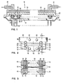
- Fig. 1 illustrates a semiconductor package 10 and the association of the thermal conduction element 20 of the invention.
- Package 10 has a dielectric substrate 12 containing a metallurgy pattern, either within or on the top surface that interconnects semiconductor devices 14 with each other and to pins 16 protruding from the bottom surface of substrate 12.
- the devices 14 are joined to the metallurgy pattern in or on substrate 12 by solder bonds 18.
- a cover element 22 is positioned over devices 14 with a surface 24 in spaced relation to the top surfaces of devices 14.
- a flange member 26, secured or brazed to substrate 12, is joined to cap 22.
- a cold plate 28 with passages 30 and inlet 32 and outlet 34 is mounted over cap 22 for the purpose of removing heat from the cap and from the devices 14.
- a cooling fluid is introduced into inlet 32 and removed through outlet 34.
- the cap 22 can be provided with fins ' or the like, as an alternative to the cooling plate 28.
- the thermal element 20 of my invention provides a thermal path from device 14 to the cap having an overall low thermal resistance that, in use, will provide dependable, consistent cooling of the devices during operation.
- Element 20 has a first set of flat, thin, flexible leaf elements 36 with spacer elements 38 disposed between the elements.
- the leaf elements and spacers are maintained in rigid relation by a pair of bolts or rivets 40.
- a second set of flat, thin, flexible leaf elements 42, separated by spacer elements 44, also with portions extending beyond the spacer elements, are interleaved with the leaf elements 36.
- Leaf elements 42 and spacer elements 44 are maintained in rigid relation by a pair of rivets or bolts 40.
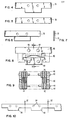
- Figs. 4 and 5 illustrate the shape of leaf elements 36 and spacer elements 38.
- leaf and spacer elements 42 and 44 have the same configuration as the leaf and spacer elements 36 and 38.
- each end of the set of leaves there is provided on each end of the set of leaves a pair of end plates 46 and 48 as shown in Fig. 2.
- the end plates are secured to the sets of leaf elements by rivets 40.
- End plate 46 has two downwardly spaced extensions 50 terminating in an inwardly extending projection 52.
- End plate 48 has outwardly extending projections 54 that interact with projections 52 and prevent the first and second sets of leaf elements from separating.
- the leaf element sets are free to slide longitudinally relative to each other permitting the opposed flat surfaces 56 and 58 to be positioned in varying distances from each other.
- the flexible nature of the leaf elements 36 and 42 permit limited tilting action of surfaces 56 and 58.
- a spring 60 is provided which engages the opposing end plates 46 and 48, and biases the sets of leaf elements in outward extending relation.
- thermal bridge element 20 in the position shown in Fig. 1 with the surface 56 in contact with underside surface 24 of cap 22, and the surface 58-in contact with the device conducts heat from the device to the cold plate 28.
- Bridge element 20 is adapted to accommodate for variations in spacing between the top surface of device 14 and surface 24 of cap 22. It is also capable of accommodating for tilting of chip 14 due to variations in solder bonds 18.
- the thermal efficiency of the system can be further enhanced by soldering surface 56 and 58 to the back side of the cap and the device or providing the suitable grease or other type of material at the interfaces.
- the size and shape of the thermal bridge element 20 will depend on the spacing of devices 14 and the sizes of the devices.
- the spacing of devices 14 is generally the determining factor in setting the size of the bridge elements. If the spacing of devices 14 is very close, the surface area of surface 56 must be accommodated to the surface area available.
- the material used in leaf elements 36 and 42 should preferably be capable of effectively conducting heat, i.e. have a high thermal conductivity.
- the leaf elements should be sufficiently flexible to accommodate for tilting of the bottom surface 58 relative to top surface 56.
- the thickness of leaf element 36 can be of any suitable thickness, preferably for semiconductor chip cooling applications from 5 to 127 ⁇ m (0.2 to 5.0 mils), more preferably from 18 to 25 pm (0.7 to 1.0 mil).
- the material of the leaf elements is preferably copper, silver, aluminum or alloys thereof which do not materially affect the thermal conductivity but impart more spring resilience to the material.
- the spacer element 38 and 44 is approximately twice the thickness of the leaf element 36.
- a preferred material for leaf elements 36 and 42 is a zirconium-copper alloy consisting of 99.8% copper and 0.2% zirconium.
- a leaf element spacer combination 70 can be formed by shaping a single piece of flat stock in the configuration illustrated in Fig. 7 where the spacing portion consists of two folded- over portions 72.
- FIG. 8 and 9 An alternate spring arrangement is illustrated in Figs. 8 and 9 of the drawings.
- the leaf elements and end plates are similar to that illustrated and explained in Figs. 2 and 3.
- Spring 80 is disposed between surfaces 82 and 84 of end plates 46 and 48 as indicated in Fig. 8.
- Spring 80 biases the sets of leaf
- a preferred technique for fabricating the thermal bridge elements 20 of the invention consists of initially shaping elongated strips 86 of thermally conductive material having the general shape illustrated in Fig. 10. A similar strip is assembled in opposed relation with the end portions 90 in overlapping alternating relation. At the same time, the spacers are also assembled until the desired width of the element is built up. At this time, the strips 86 are severed on lines 92 and holes 94 drilled. End plates 46 and 48 are positioned on each end of the stacked assembly, rivets 40 put in place and secured. Biasing spring, either of the type illustrated in Figs. 2 and 3 or in Figs. 8 and 9, are then inserted in place and the assembly is ready for use. If desirable,the end surfaces of the assembly., i.e. 56 and 58, can be ground or polished. The spacing and leaf elements 70 can be used in the same manner described if such embodiment is desired.
Abstract
Description
- This invention relates to structures for the dissipation of thermal energy generated by semiconductor devices. More particularly; the present invention relates to conduction elements for cooling semiconductor devices in single device or multi-device integrated circuit package assemblies where the devices are mounted on substrates with solder bonds, and the caps are mounted in close proximity to the back sides of the devices.
- The high circuit densities in modern integrated circuit semiconductor devices require that the heat generated by their operation be efficiently removed in order to maintain the temperature of the devices within limits that will keep the operating parameters of the devices within pre-determined ranges, and also prevent destruction of the device by overheating. The problems of heat removal are increased when the device is connected to the supporting substrate with solder terminals that electrically connect the device to appropriate terminals on the substrate. On such solder bonded devices, the heat transfer that can be accomplished through the solder bonds is limited, as compared to back bonded devices. Cooling of the semiconductor devices can be achieved by immersing the devices in a suitable liquid coolant. However, these cooling techniques can result in corrosion of the device and substrate metallurgy and also present problems if the package must be reworked. Cooling can also be achieved by providing a conductive link of material, such as conductive pistons or spring elements, between the device and the cap or cold plate. These elements must be capable of forming a good interface contact over as large an area as possible in order to maintain a low thermal resistance. With cooling pistons, forming such interfaces is difficult because the devices may be tilted, resulting in an unsatisfactory point or line contact. In general, cooling pistons must be used in an atmosphere of inert gases with higher heat conductivity than air, or a grease or other conformal means be provided at the piston end/device interface. Another disadvantage is that the pistons may subject the devices being cooled to shock when the package is subjected to inertial forces. Spring elements for thermal conduction between a device and cold plate are known. A prevalent problem is designing sufficiently heavy springs that will efficiently conduct heat and yet not impose forces on the devices that will crack or chip them. The consideration becomes more severe as the tolerance of the gap between the device and cap are increased.
- The following prior art references relate to various structures for removing heat from solder bonded semiconductor devices. U.S. Patent No. 3 993 123 discloses a semiconductor package in which a movable heat conductive piston is placed in contact with the back side of a solder bonded semiconductor device to conduct heat away from the device to a cooling plate. U.S. Patents No. 4 034 468 and 4 081 825 both disclose semiconductor packages wherein a low melting point solder is provided in contact with the back side of a solder bonded device and with the module cap to remove heat from the device. U.S. Patent 4 156 458 discloses a cooling arrangement including a flexible heat conductive metallic foil bundle extending between the back side of a device and the heat sink. IBM Technical Disclosure Bulletin Vol. 21, No. 3, Aug. 1978, p. 1141 discloses a thermal shunt element disposed between a solder bonded semiconductor device and a module cap comprised of a rectangular center portion and a pair of divergent wings that contact the cap. IBM Technical Disclosure Bulletin, Vol. 20, No. 6, Nov. 1977, p. 2214 and U.S. Patent No. 4 146 458, issued 20 May 1979 disclose a plurality of preform sheets of aluminum foil nested together and disposed between solder bonded semiconductor devices and a housing to remove heat from the devices. IBM Technical Disclosure Bulletin, Vol. 19, No. 12, May 1977, p. 4683 discloses a thermal conduction bridge element between a solder bonded semiconductor device and a cap which features a plurality of interleaved relatively slidable fins. European patent application 82lQ1551.8,fi1ed 1 March 1982 discloses a thermal bridge for conducting heat from a device to the cover which includes a relatively thick metal sheet provided with cuts that define at least one tab element.
- The invention is an improved cooling element adapted to be positioned between a solder bonded semiconductor device and a module cap or cold plate to form a heat conduction bridge between the device and cap or cold plate. The cooling element has a plurality of interleaved thin plates arranged so that the ends of the element are expandable and also capable of adjusting to intimately contact the device, even though the top surface of the device is tilted relative to the cap or cold plate surface. The thermal element has a first set of flexible leaf elements, a set of spacer elements between the leaf elements, a second set of flexible leaf elements with portions thereof disposed in slidable relation to the first set of leaf elements, a second set of space elements disposed between the individual leaf elements, a means to hold the first and second leaf elements in assembled and extendable relation, and a spring to bias the leaf elements in extended relation. The thermal bridge element of the invention is sufficiently flexible to allow the ends of the element to intimately contact the back side of the device and the cover or cap, and thereby achieve a low overall thermal resistance that permits heat to be transferred from the device to the cap or cold plate.
- The details of the invention will be described in connection with the accompanying drawings in which:
- Fig. 1 is an elevational view in broken section illustrating a semiconductor package including semiconductor devices solder bonded to a substrate and a cooling plate with the thermal bridge elements disposed in operative cooling relation to the devices and cold plate.
- Fig. 2 is an elevational view in enlarged scale illustrating the structure of a thermal bridge of the invention.
- Fig. 3 is a sectional view taken on line 3-3 of Fig. 2, illustrating the interleaved structure of the thermal bridge of the invention.
- Fig. 4 is a view of a single leaf element used in the thermal bridge element of the invention.
- Fig. 5 is a view of a single spacer element.
- Fig. 6 is a view of a modified leaf element and spacer of another preferred specific embodiment of the invention.
- Fig. 7 is an end view of the leaf element of Fig. 6.
- Fig. 8 is a front view illustrating an alternate spring embodiment of the thermal element of the invention.
- Fig. 9 is a sectional view taken on line 9-9 of Fig. 8.
- Fig. 10 is a view of a continuous metal strip illustrating a preferred method of making the thermal bridge element of the invention.
- Referring to the drawings, Fig. 1 illustrates a
semiconductor package 10 and the association of thethermal conduction element 20 of the invention.Package 10 has adielectric substrate 12 containing a metallurgy pattern, either within or on the top surface that interconnectssemiconductor devices 14 with each other and to pins 16 protruding from the bottom surface ofsubstrate 12. - The
devices 14 are joined to the metallurgy pattern in or onsubstrate 12 bysolder bonds 18. Acover element 22 is positioned overdevices 14 with asurface 24 in spaced relation to the top surfaces ofdevices 14. Aflange member 26, secured or brazed tosubstrate 12, is joined tocap 22. Acold plate 28 withpassages 30 andinlet 32 andoutlet 34 is mounted overcap 22 for the purpose of removing heat from the cap and from thedevices 14. In use, a cooling fluid is introduced intoinlet 32 and removed throughoutlet 34. In contrast, thecap 22 can be provided with fins ' or the like, as an alternative to thecooling plate 28. Thethermal element 20 of my invention provides a thermal path fromdevice 14 to the cap having an overall low thermal resistance that, in use, will provide dependable, consistent cooling of the devices during operation. - Referring now to Figs. 2 and 3, there is depicted a thermal bridge element of the invention.
Element 20 has a first set of flat, thin,flexible leaf elements 36 withspacer elements 38 disposed between the elements. The leaf elements and spacers are maintained in rigid relation by a pair of bolts orrivets 40. As indicated in Fig. 3,a portion of each of theleaf elements 36 extend well beyond thespacer elements 38. A second set of flat, thin,flexible leaf elements 42, separated byspacer elements 44, also with portions extending beyond the spacer elements, are interleaved with theleaf elements 36.Leaf elements 42 and spacer elements 44 are maintained in rigid relation by a pair of rivets or bolts 40. Figs. 4 and 5 illustrate the shape ofleaf elements 36 andspacer elements 38. Preferably leaf andspacer elements spacer elements - In order to prevent the first and second sets of leaf elements from separating, there is provided on each end of the set of leaves a pair of
end plates rivets 40.End plate 46 has two downwardly spacedextensions 50 terminating in an inwardly extendingprojection 52.End plate 48 has outwardly extendingprojections 54 that interact withprojections 52 and prevent the first and second sets of leaf elements from separating. As indicated in Fig. 3, the leaf element sets are free to slide longitudinally relative to each other permitting the opposedflat surfaces leaf elements surfaces spring 60 is provided which engages theopposing end plates thermal bridge element 20 in the position shown in Fig. 1 with thesurface 56 in contact withunderside surface 24 ofcap 22, and the surface 58-in contact with the device conducts heat from the device to thecold plate 28.Bridge element 20 is adapted to accommodate for variations in spacing between the top surface ofdevice 14 andsurface 24 ofcap 22. It is also capable of accommodating for tilting ofchip 14 due to variations insolder bonds 18. The thermal efficiency of the system can be further enhanced by solderingsurface - The size and shape of the
thermal bridge element 20 will depend on the spacing ofdevices 14 and the sizes of the devices. The spacing ofdevices 14 is generally the determining factor in setting the size of the bridge elements. If the spacing ofdevices 14 is very close, the surface area ofsurface 56 must be accommodated to the surface area available. The material used inleaf elements bottom surface 58 relative totop surface 56. In general, the thickness ofleaf element 36 can be of any suitable thickness, preferably for semiconductor chip cooling applications from 5 to 127 µm (0.2 to 5.0 mils), more preferably from 18 to 25 pm (0.7 to 1.0 mil). The material of the leaf elements is preferably copper, silver, aluminum or alloys thereof which do not materially affect the thermal conductivity but impart more spring resilience to the material. In general, thespacer element leaf element 36. A preferred material forleaf elements - An alternative embodiment structure of the combination of leaf elements and spacers is shown in Figs. 6 and 7. A leaf
element spacer combination 70 can be formed by shaping a single piece of flat stock in the configuration illustrated in Fig. 7 where the spacing portion consists of two folded- overportions 72. - An alternate spring arrangement is illustrated in Figs. 8 and 9 of the drawings. The leaf elements and end plates are similar to that illustrated and explained in Figs. 2 and 3.
Spring 80 is disposed betweensurfaces end plates Spring 80 biases the sets of leaf -
elements spring 60. - A preferred technique for fabricating the
thermal bridge elements 20 of the invention consists of initially shaping elongated strips 86 of thermally conductive material having the general shape illustrated in Fig. 10. A similar strip is assembled in opposed relation with theend portions 90 in overlapping alternating relation. At the same time, the spacers are also assembled until the desired width of the element is built up. At this time, the strips 86 are severed onlines 92 and holes 94 drilled.End plates leaf elements 70 can be used in the same manner described if such embodiment is desired.
Claims (10)
Applications Claiming Priority (2)
| Application Number | Priority Date | Filing Date | Title |
|---|---|---|---|
| US06/289,025 US4498530A (en) | 1981-08-03 | 1981-08-03 | Flexible thermal conduction element for cooling semiconductor devices |
| US289025 | 1981-08-03 |
Publications (3)
| Publication Number | Publication Date |
|---|---|
| EP0071709A2 true EP0071709A2 (en) | 1983-02-16 |
| EP0071709A3 EP0071709A3 (en) | 1984-12-19 |
| EP0071709B1 EP0071709B1 (en) | 1987-09-02 |
Family
ID=23109691
Family Applications (1)
| Application Number | Title | Priority Date | Filing Date |
|---|---|---|---|
| EP82104819A Expired EP0071709B1 (en) | 1981-08-03 | 1982-06-02 | Flexible thermal conduction element for cooling semiconductor devices |
Country Status (4)
| Country | Link |
|---|---|
| US (1) | US4498530A (en) |
| EP (1) | EP0071709B1 (en) |
| JP (1) | JPS5823463A (en) |
| DE (1) | DE3277157D1 (en) |
Cited By (2)
| Publication number | Priority date | Publication date | Assignee | Title |
|---|---|---|---|---|
| EP0169270A1 (en) * | 1983-12-14 | 1986-01-29 | Hitachi, Ltd. | Cooling device of semiconductor chips |
| EP0454603A2 (en) * | 1990-03-30 | 1991-10-30 | International Business Machines Corporation | High conduction flexible fin cooling module |
Families Citing this family (47)
| Publication number | Priority date | Publication date | Assignee | Title |
|---|---|---|---|---|
| USRE35721E (en) * | 1983-12-14 | 1998-02-03 | Hitachi, Ltd. | Cooling device of semiconductor chips |
| US4669535A (en) * | 1985-08-07 | 1987-06-02 | North American Specialties Corp. | Heat sink formed of stacked fin elements |
| US5083373A (en) * | 1986-04-25 | 1992-01-28 | Hamburgen William R | Method for providing a thermal transfer device for the removal of heat from packaged elements |
| US4800956A (en) * | 1986-04-25 | 1989-01-31 | Digital Equipment Corporation | Apparatus and method for removal of heat from packaged element |
| US4768581A (en) * | 1987-04-06 | 1988-09-06 | International Business Machines Corporation | Cooling system for semiconductor modules |
| US5052481A (en) * | 1988-05-26 | 1991-10-01 | International Business Machines Corporation | High conduction cooling module having internal fins and compliant interfaces for vlsi chip technology |
| JP2507561B2 (en) * | 1988-10-19 | 1996-06-12 | 株式会社日立製作所 | Semiconductor cooling system |
| CA2002213C (en) * | 1988-11-10 | 1999-03-30 | Iwona Turlik | High performance integrated circuit chip package and method of making same |
| US4882654A (en) * | 1988-12-22 | 1989-11-21 | Microelectronics And Computer Technology Corporation | Method and apparatus for adjustably mounting a heat exchanger for an electronic component |
| JP2675173B2 (en) * | 1990-03-02 | 1997-11-12 | 株式会社日立製作所 | Electronic device cooling system |
| US5377077A (en) * | 1990-08-01 | 1994-12-27 | Staktek Corporation | Ultra high density integrated circuit packages method and apparatus |
| JPH04196395A (en) * | 1990-11-28 | 1992-07-16 | Hitachi Ltd | Electronic computer and cooling device thereof |
| US5774334A (en) * | 1994-08-26 | 1998-06-30 | Hitachi, Ltd. | Low thermal resistant, fluid-cooled semiconductor module |
| US5983997A (en) * | 1996-10-17 | 1999-11-16 | Brazonics, Inc. | Cold plate having uniform pressure drop and uniform flow rate |
| US6026895A (en) * | 1998-02-06 | 2000-02-22 | Fujitsu Limited | Flexible foil finned heatsink structure and method of making same |
| US6179047B1 (en) * | 1998-12-10 | 2001-01-30 | Unisys Corporation | Mechanical assembly for regulating the temperature of an electronic device which incorporates at least two leaf springs for self-alignment plus a low initial contact force and a low profile |
| US6741480B2 (en) | 1999-07-15 | 2004-05-25 | Incep Technologies, Inc. | Integrated power delivery with flex circuit interconnection for high density power circuits for integrated circuits and systems |
| US6623279B2 (en) | 1999-07-15 | 2003-09-23 | Incep Technologies, Inc. | Separable power delivery connector |
| US6452113B2 (en) | 1999-07-15 | 2002-09-17 | Incep Technologies, Inc. | Apparatus for providing power to a microprocessor with integrated thermal and EMI management |
| US20030214800A1 (en) * | 1999-07-15 | 2003-11-20 | Dibene Joseph Ted | System and method for processor power delivery and thermal management |
| US6356448B1 (en) | 1999-11-02 | 2002-03-12 | Inceptechnologies, Inc. | Inter-circuit encapsulated packaging for power delivery |
| US6801431B2 (en) * | 1999-07-15 | 2004-10-05 | Incep Technologies, Inc. | Integrated power delivery and cooling system for high power microprocessors |
| US20030156400A1 (en) * | 1999-07-15 | 2003-08-21 | Dibene Joseph Ted | Method and apparatus for providing power to a microprocessor with intergrated thermal and EMI management |
| US6304450B1 (en) | 1999-07-15 | 2001-10-16 | Incep Technologies, Inc. | Inter-circuit encapsulated packaging |
| US6947293B2 (en) * | 1999-07-15 | 2005-09-20 | Incep Technologies | Method and apparatus for providing power to a microprocessor with integrated thermal and EMI management |
| US6618268B2 (en) | 1999-07-15 | 2003-09-09 | Incep Technologies, Inc. | Apparatus for delivering power to high performance electronic assemblies |
| US6556455B2 (en) | 1999-07-15 | 2003-04-29 | Incep Technologies, Inc. | Ultra-low impedance power interconnection system for electronic packages |
| US6847529B2 (en) * | 1999-07-15 | 2005-01-25 | Incep Technologies, Inc. | Ultra-low impedance power interconnection system for electronic packages |
| US7167379B2 (en) * | 2001-02-16 | 2007-01-23 | Dibene Ii Joseph T | Micro-spring interconnect systems for low impedance high power applications |
| US6845013B2 (en) * | 2002-03-04 | 2005-01-18 | Incep Technologies, Inc. | Right-angle power interconnect electronic packaging assembly |
| US6684501B2 (en) * | 2002-03-25 | 2004-02-03 | International Business Machines Corporation | Foil heat sink and a method for fabricating same |
| US6910271B2 (en) * | 2002-10-29 | 2005-06-28 | Hewlett-Packard Development Company, L.P. | Mechanical highly compliant thermal interface pad |
| US6778393B2 (en) * | 2002-12-02 | 2004-08-17 | International Business Machines Corporation | Cooling device with multiple compliant elements |
| US7188667B2 (en) * | 2004-07-29 | 2007-03-13 | International Business Machines Corporation | Liquid cooling structure for electronic device |
| US7193318B2 (en) * | 2004-08-18 | 2007-03-20 | International Business Machines Corporation | Multiple power density chip structure |
| US7277291B2 (en) * | 2005-08-08 | 2007-10-02 | Verifone Holdings, Inc. | Thermal transfer device |
| EP2247172B1 (en) * | 2009-04-27 | 2013-01-30 | Siemens Aktiengesellschaft | Cooling system, cooling board and assembly with cooling system |
| US9312571B2 (en) | 2014-03-19 | 2016-04-12 | Ford Global Technologies, Llc | Traction battery thermal plate with flexible bladder |
| US9912107B2 (en) | 2014-04-01 | 2018-03-06 | Te Connectivity Corporation | Plug and receptacle assembly having a thermally conductive interface |
| US9435590B2 (en) | 2014-04-07 | 2016-09-06 | Microsoft Technology Licensing, Llc | Thin heat transfer device for thermal management |
| CN110413079B (en) * | 2018-04-28 | 2022-09-09 | 伊姆西Ip控股有限责任公司 | Heat sink for an expansion card, expansion card comprising a heat sink and associated manufacturing method |
| US11177192B2 (en) * | 2018-09-27 | 2021-11-16 | Taiwan Semiconductor Manufacturing Company, Ltd. | Semiconductor device including heat dissipation structure and fabricating method of the same |
| US11439042B2 (en) * | 2019-09-12 | 2022-09-06 | Te Connectivity Solutions Gmbh | Heat exchange assembly for a communication system |
| US11486661B2 (en) * | 2020-05-28 | 2022-11-01 | Te Connectivity Solutions Gmbh | Thermal bridge for an electrical component |
| US11240934B1 (en) * | 2020-07-22 | 2022-02-01 | TE Connectivity Services Gmbh | Thermal bridge for an electrical component |
| US20210333848A1 (en) * | 2021-07-07 | 2021-10-28 | Intel Corporation | Expandable thermal solution for laptops |
| US11778786B2 (en) * | 2021-12-22 | 2023-10-03 | Te Connectivity Solutions Gmbh | Thermal bridge for an electrical component |
Citations (3)
| Publication number | Priority date | Publication date | Assignee | Title |
|---|---|---|---|---|
| US4245273A (en) * | 1979-06-29 | 1981-01-13 | International Business Machines Corporation | Package for mounting and interconnecting a plurality of large scale integrated semiconductor devices |
| US4263965A (en) * | 1980-01-21 | 1981-04-28 | International Business Machines Corporation | Leaved thermal cooling module |
| EP0031448A2 (en) * | 1979-12-17 | 1981-07-08 | International Business Machines Corporation | Thermal conduction module for integrated circuit chips |
Family Cites Families (1)
| Publication number | Priority date | Publication date | Assignee | Title |
|---|---|---|---|---|
| US4226281A (en) * | 1979-06-11 | 1980-10-07 | International Business Machines Corporation | Thermal conduction module |
-
1981
- 1981-08-03 US US06/289,025 patent/US4498530A/en not_active Expired - Fee Related
-
1982
- 1982-05-20 JP JP57084103A patent/JPS5823463A/en active Granted
- 1982-06-02 DE DE8282104819T patent/DE3277157D1/en not_active Expired
- 1982-06-02 EP EP82104819A patent/EP0071709B1/en not_active Expired
Patent Citations (3)
| Publication number | Priority date | Publication date | Assignee | Title |
|---|---|---|---|---|
| US4245273A (en) * | 1979-06-29 | 1981-01-13 | International Business Machines Corporation | Package for mounting and interconnecting a plurality of large scale integrated semiconductor devices |
| EP0031448A2 (en) * | 1979-12-17 | 1981-07-08 | International Business Machines Corporation | Thermal conduction module for integrated circuit chips |
| US4263965A (en) * | 1980-01-21 | 1981-04-28 | International Business Machines Corporation | Leaved thermal cooling module |
Non-Patent Citations (1)
| Title |
|---|
| IBM TECHNICAL DISCLOSURE BULLETIN, vol. 19, no. 12, May 1977, page 4683, New York, US; E.L. DOMBROSKI et al.: "Thermal conduction stud" * |
Cited By (3)
| Publication number | Priority date | Publication date | Assignee | Title |
|---|---|---|---|---|
| EP0169270A1 (en) * | 1983-12-14 | 1986-01-29 | Hitachi, Ltd. | Cooling device of semiconductor chips |
| EP0454603A2 (en) * | 1990-03-30 | 1991-10-30 | International Business Machines Corporation | High conduction flexible fin cooling module |
| EP0454603A3 (en) * | 1990-03-30 | 1991-11-06 | International Business Machines Corporation | High conduction flexible fin cooling module |
Also Published As
| Publication number | Publication date |
|---|---|
| EP0071709A3 (en) | 1984-12-19 |
| DE3277157D1 (en) | 1987-10-08 |
| US4498530A (en) | 1985-02-12 |
| EP0071709B1 (en) | 1987-09-02 |
| JPS5823463A (en) | 1983-02-12 |
| JPS6238859B2 (en) | 1987-08-20 |
Similar Documents
| Publication | Publication Date | Title |
|---|---|---|
| EP0071709B1 (en) | Flexible thermal conduction element for cooling semiconductor devices | |
| EP0111709B1 (en) | Telescoping thermal conduction element for cooling semiconductor devices | |
| US4442450A (en) | Cooling element for solder bonded semiconductor devices | |
| EP0097782B1 (en) | Thermal conduction bridge element for semiconductor device packages | |
| US4415025A (en) | Thermal conduction element for semiconductor devices | |
| US6554060B2 (en) | Heat sink with fins | |
| EP0140119B1 (en) | Method of making a chip cooling device | |
| US6698500B2 (en) | Heat sink with fins | |
| EP0088246B1 (en) | Telescopic thermal conduction element for semiconductor devices | |
| JPS6238861B2 (en) | ||
| US5945905A (en) | High power resistor | |
| US5131456A (en) | Bimetallic insert fin for high conduction cooling structure | |
| US6873028B2 (en) | Surge current chip resistor | |
| EP0146463B1 (en) | Compliant lead frame for surface mount semiconductor packages | |
| GB2300975A (en) | Heatsinks having fin members joined to a base | |
| JP3865179B2 (en) | Power electronic circuit device and manufacturing method thereof | |
| CN114974761A (en) | High power chip resistor | |
| JPS58151036A (en) | Semiconductor device |
Legal Events
| Date | Code | Title | Description |
|---|---|---|---|
| PUAI | Public reference made under article 153(3) epc to a published international application that has entered the european phase |
Free format text: ORIGINAL CODE: 0009012 |
|
| AK | Designated contracting states |
Designated state(s): DE FR GB |
|
| 17P | Request for examination filed |
Effective date: 19830621 |
|
| PUAL | Search report despatched |
Free format text: ORIGINAL CODE: 0009013 |
|
| AK | Designated contracting states |
Designated state(s): DE FR GB |
|
| 17Q | First examination report despatched |
Effective date: 19860930 |
|
| GRAA | (expected) grant |
Free format text: ORIGINAL CODE: 0009210 |
|
| AK | Designated contracting states |
Kind code of ref document: B1 Designated state(s): DE FR GB |
|
| REF | Corresponds to: |
Ref document number: 3277157 Country of ref document: DE Date of ref document: 19871008 |
|
| ET | Fr: translation filed | ||
| PLBE | No opposition filed within time limit |
Free format text: ORIGINAL CODE: 0009261 |
|
| STAA | Information on the status of an ep patent application or granted ep patent |
Free format text: STATUS: NO OPPOSITION FILED WITHIN TIME LIMIT |
|
| 26N | No opposition filed | ||
| PGFP | Annual fee paid to national office [announced via postgrant information from national office to epo] |
Ref country code: GB Payment date: 19920506 Year of fee payment: 11 |
|
| PGFP | Annual fee paid to national office [announced via postgrant information from national office to epo] |
Ref country code: FR Payment date: 19920601 Year of fee payment: 11 |
|
| PGFP | Annual fee paid to national office [announced via postgrant information from national office to epo] |
Ref country code: DE Payment date: 19920619 Year of fee payment: 11 |
|
| PG25 | Lapsed in a contracting state [announced via postgrant information from national office to epo] |
Ref country code: GB Effective date: 19930602 |
|
| GBPC | Gb: european patent ceased through non-payment of renewal fee |
Effective date: 19930602 |
|
| PG25 | Lapsed in a contracting state [announced via postgrant information from national office to epo] |
Ref country code: FR Effective date: 19940228 |
|
| PG25 | Lapsed in a contracting state [announced via postgrant information from national office to epo] |
Ref country code: DE Effective date: 19940301 |
|
| REG | Reference to a national code |
Ref country code: FR Ref legal event code: ST |