EP0071315B1 - Digital data apparatus with peripheral unit select - Google Patents
Digital data apparatus with peripheral unit select Download PDFInfo
- Publication number
- EP0071315B1 EP0071315B1 EP82200940A EP82200940A EP0071315B1 EP 0071315 B1 EP0071315 B1 EP 0071315B1 EP 82200940 A EP82200940 A EP 82200940A EP 82200940 A EP82200940 A EP 82200940A EP 0071315 B1 EP0071315 B1 EP 0071315B1
- Authority
- EP
- European Patent Office
- Prior art keywords
- address
- code
- codes
- bit
- unit
- Prior art date
- Legal status (The legal status is an assumption and is not a legal conclusion. Google has not performed a legal analysis and makes no representation as to the accuracy of the status listed.)
- Expired - Lifetime
Links
Images


Classifications
-
- G—PHYSICS
- G06—COMPUTING OR CALCULATING; COUNTING
- G06F—ELECTRIC DIGITAL DATA PROCESSING
- G06F12/00—Accessing, addressing or allocating within memory systems or architectures
- G06F12/02—Addressing or allocation; Relocation
- G06F12/06—Addressing a physical block of locations, e.g. base addressing, module addressing, memory dedication
- G06F12/0646—Configuration or reconfiguration
- G06F12/0684—Configuration or reconfiguration with feedback, e.g. presence or absence of unit detected by addressing, overflow detection
Definitions
- This invention relates to digital data apparatus of a character comprising a data processing unit and a plurality of peripheral units which are selectively addressable by addresser means in the processing unit with multi-bit address codes over an address bus for the transfer over a data bus of digital data between the data processing unit and an addressed peripheral unit, each of which peripheral units is adapted to store in a respective storage location a unique identification code which is provided by means in the data processing unit and which corresponds to an address code for the peripheral unit.
- the invention relates more particularly to specific apparatus of the above character in which the peripheral units are random access memory units, although it will be apparent to one skilled in the art that the application of the invention to such apparatus having other forms of peripheral unit is possible.
- a data processing unit is implemented as an integrated circuit in a package, with connection to one or more random access memory units external to the integrated circuit package being effected by way of external connecting pins on the package.
- connection between the processing unit and different numbers of memory units may be a requirement to accommodate connection between the processing unit and different numbers of memory units, according to particular uses of the apparatus.
- the processing unit may know which memory unit address codes are valid for selectively addressing memory units because respective memory units have been provided in respect of them, and which memory unit address codes are invalid because no memory units have been provided in respect of them.
- the memory unit address codes are unique multi-bit codes which are fed by the processing unit over an address bus to a decoder which in respect of each code produces a respective select signal for selecting a particular one of the memory units for interrogation.
- the provision of the decoder ensures that each address cdde does select uniquely only one memory unit (when provided).
- Another prior art example of this method of addressing using a unique multi-bit address code to produce a respective select signal is given in IBM Technical Disclosure Bulletin, Vol. 18, No. 3, August 1975, pages 878/9 in the article "Basic Storage Module Selection Check".
- a "command" signal is issued to a particular BSM (Basic Storage Module) by transmitting that "command” signal over a transfer bus to that BSM (and possibly other BSM's) and activating the particular BSM by a "command select” signal applied to that BSM only.
- the "command” signal includes a module address which is stored in an identifier section of each BSM when the "command" signal is applied to the BSM's.
- the module address is also decoded by a system controller to produce a unique "command select" signal for the BSM to which the module address pertains.
- the BSM concerned On receiving the "command select” signal the BSM concerned compares the module address which is stored in its identifier section with a module identification code which corresponds to the module address and is pre-stored in the module.
- the "command" signal is executed or not according as the module address matches or does not match the pre-stored module identification code.
- digital data apparatus of the character specified in the opening paragraph of the specification is characterised in that said address code has a bit of a particular one value in a given bit position and the address bus line for that bit position is connected only to the peripheral unit concerned, whereby said bit constitutes a select signal for the peripheral unit; in that said data processing unit includes comparison means for comparing an identification code which is received by it from an addressed peripheral unit with the address code having at least said one bit of a particular value used to address the peripheral unit, in order to validate or not that peripheral unit according as there is correspondence or not between the compared codes; and in that there is included in the data processing unit flag bit producing means for including as part of the identification code for each peripheral unit flag bits which signify the number of bits of said particular one value contained in the address code part of the identification code, said flag bit producing means also being used to add to an address code which is to be compared by the comparison means with a received identification code flag bits which signify the number of bits of said particular one value in that address code.
- the comparison means can be prevented from validating erroneously two or more peripheral units which have been selected at the same time by an invalid address code containing more than one bit of said particular one value.
- the flag bit parts can be chosen. so as always to identify an invalid address code.
- each peripheral unit can comprise two or more sub-units.
- each sub-unit has its own identification code recorded in a respective storage location therein, which identification codes for all the sub-units of a peripheral unit have said bit of a particular one value in the same given bit position, this bit in the corresponding address codes constituting a common select signal for the peripheral unit.
- This use of the identification codes has the advantage that the digital data apparatus can have peripheral units which contain different numbers of sub-units.
- bits in the sub-unit individual identification codes which do not serve as such common select signals in the corresponding address codes can be used singly or in combination to selectthe sub-units of any selected peripheral unit in accordance with their different possible values. This use of these other bits has the advantage that it provides a simple means of sub-unit identification within a peripheral unit when the peripheral units all have the same number of sub-units.
- the identification codes can be recorded in respective storage locations using a writing operation by which writing means in the data processing unit applies all the possible address codes to the address bus in turn in a special sequence, and for each address code the writing means also applies the code, together with the associated flag bit(s) from the flag bit producing means (FLG), as data for recording into the storage location of each addressed peripheral unit or sub-unit, the special writing sequence being such that the address code which has all its bits of said one value is written first, followed by the address codes which have all their bits except one of said one value, followed by the address codes which have all their bits except two of said one value, and so on, the sequence finishing with the address code which has none of its bits of said one value.
- FLG flag bit producing means
- This use of the special writing sequence has the advantage that the data processing unit can provide for each peripheral unit or sub-unit an identification code which identifies uniquely the unit irrespective of how many units are provided out of the total possible. This is because in the writing sequence the address codes which can select more than one peripheral unit occur before the address codes which can select only one peripheral unit, and the latter codes over-write progressively the former codes in the storage locations during the writing sequence, until there is finally written into the storage locations respective identification codes corresponding to address codes which can select only one peripheral unit or sub-unit.
- memory is connected to the processing unit as a plurality of memory units each of the same number of storage bytes, this number corresponding to the smallest size of memory unit which is envisaged.
- Such a smallest size of memory unit will be deemed to be a "chapter" of memory for the purposes of the present description.
- These memory units can be respective memory devices each containing one "chapter” of memory, or a larger size memory device can be considered as a plurality of memory units each containing one "chapter” of memory. Each such larger size memory device would always contain an integral number of "chapters" of memory.
- a "chapter” can be 1024 bytes of 8 bits, and, as will be described with reference to Figures 1 to 3, Random Access Memory (RAM) devices of 1, 2 and 4 chapter sizes could be available for use.
- RAM Random Access Memory
- the digital apparatus shown in each of Figures 1 to 3 comprises an integrated circuit IC containing a processing unit PU and an interface circuit INTF which are interconnected internally in the integrated circuit IC.
- the integrated circuit IC has sixteen external connecting pins CP1 to CP16 by which external connection is made to RAM equipment RM which contains different numbers and configurations of memory units in the three Figures, as will be described. (The integrated circuit IC would, of course, have further external connecting pins (not shown) for applying thereto supply voltages, and for clock and control signals, etc.).
- a 6-line address bus consisting of parallel address lines CA1 to CA6 extends between the RAM equipment RM and the connecting pins CP1 to CP6.
- Binary 6-bit chapter address codes applied from the processing unit PU over this address bus will select certain of the memory units in the RAM equipment RM.
- These 6-bit address codes constitute valid or invalid address codes, respectively, according as they can select only one, or more than one, memory unit.
- the first eight (BA1 to BA8) also serve as data lines DT1 to DT8 which form an 8-line data bus for the transfer of data between the integrated circuit IC and the RAM equipment RM. The direction of data transfer is controlled from the processing unit PU.
- the address/data bus (BA1 to BA10, DT1 to DT8) is used on a multiplex basis in different time intervals for either byte addressing or data transfer, this multiplexing also being controlled from the processing unit PU.
- a separate 8-line data bus can be provided, but this requires an additional eight connecting pins on the integrated circuit IC.
- the RAM equipment RM comprises six discrete RAM devices RM1(1) to RM6(1) each of which has a capacity of one memory unit.
- Each of the devices RM1(1) to RM6(1) has a so-called "chip" select terminal TCS, and the address lines CA1 to CA6 are connected respectively to these terminals.
- the particular RAM device to which that address line is connected is selected for data transfer. Byte addressing and data transfer can thereafter be effected over the address/data lines BA1 to BA10/DT1 to DT8.
- circuits which are used for "chip" selecting, byte addressing and data transfer are readily available and will not, therefore, be described in the present specification in respect of the apparatus shown in Figures 1 to 3; particularly also as a description of such circuit details is not necessary for an understanding of the present invention.
- the RAM equipment RM of the apparatus shown in Figure 2 comprises five discrete RAM devices RM1(2) to RM5(2) each of which has a capacity of two memory units.
- the address lines CA1 to CA5 are connected to the "chip" select terminal of the respective RAM devices, while the address line CA6 is connected to a 1-out-of-2 "unit" select terminal UST of each device and is used to determine which of the two memory units of a selected RAM device is to be chosen, according as this latter address line CA6 is made active high (binary level "1") or active low (binary level "0").
- the RAM equipment RM of the apparatus shown in Figure 3 comprises four discrete RAM devices RM1(4) to RM4(4) each of which has a capacity of four memory units.
- the address lines CA1 to CA4 are connected to the "chip" select terminal TCS of the respective RAM devices, while the address lines CA5 and CA6 are connected respectively to 1-out-of-4 "unit" select terminals UST1 and UST2 of each device and are used to determine, in accordance with their unique binary level combinations (00, 01, 10 and 11), which one of the four memory units of a selected RAM device is to be chosen.
- the processing unit PU includes a chapter addresser C/ADD for producing the 6-bit chapter address codes for application via a 6-bit connection CY/AD to the address bus CA1 to CA6 by way of a multiplexer MUX1 in its unswitched state.
- a logic circuit LC of the processing unit controls the operation of the chapter addresser C/ADD over a control lead or leads CAC.
- a possible means-of implementation and control would be for the logic circuit LC to supply stepping pulses to a counter, which forms the chapter addresser, until a count corresponding to a required address code is reached, following which this address code would be held latched for application to the address bus.
- these 6-bit address codes are produced periodically in a special sequence by a chapter address sequencer C/SEQ in response to a control signal from the logic circuit LC on a control lead SAC.
- a convenient means of implementation and control would be for the logic circuit LC to supply stepping pulses to a counter which forms the chapter address sequencer, but with the counter having its counting stages interconnected with appropriate gating and feed-back paths to produce a count according to the special sequence instead of its natural count.
- the sequenced address codes are applied to the address bus CA1 to CA6 by way of the multiplexer MUX1 in its switched state, the switching of this multiplexer being effected by the control signal on the control lead SAC.
- the sequenced address codes are also applied by way of another multiplexer MUX2, in its switched state, to the data bus DT1 to DT8 to be recorded with the flag bits as identification codes in a specially allocated storage location (byte) in each of those memory units which are provided.
- the specially allocated storage location is the same byte in each memory unit and is identified, both for writing into and for reading from, by the appropriate byte address code as produced by a byte addresser B/ADD, which produces the 10-bit byte address codes on a 10-bit connection BY/AD for application to the address bus BA1 to BA10, in response to a RAM finder signal from the logic circuit LC on a control lead RF.
- the logic circuit LC otherwise controls the byte addresser B/ADD for byte addressing during normal memory unit operation over a control lead BAC. Also, for normal memory unit operation, data written into a memory unit storage byte is fed from the logic circuit LC by way of the multiplexer MUX2, in its unswitched state, over an 8-bit connection DAT/OT to the data bus DT1 to DT8: data read from a memory unit storage byte is fed to the logic circuit LC from the data bus DT1 to DT8 over an 8-bit connection DAT/IN.
- the leads RD, WR and ALE signify the "read”, "write” and "address latch enable" control which is exercised in conventional known manner by the logic circuit LC on the memory units.
- the processing unit PU also includes a comparator COMP and a flag bit producer FLG.
- the chapter address codes at the output of the multiplexer MUX1 are applied to both the comparator COMP and to the flag bit producer FLG, which latter is responsive to an applied chapter address code to produce two flag bits the binary value combination of which is representative of how many bits of the value which constitutes a "chip" select signal are contained in the address code.
- These two flag bits are applied to the comparator COMP along with the 6-bit chapter address code.
- the 6-bit chapter address codes, along with their respective two flag bits, also form the 8-bit identification codes which are applied over the data bus DT1 to DT8 for recording in the specially allocated storage location in the memory units.
- a chapter address code applied to the address bus CA1 to CA6 is tested for validity by the comparator COMP by comparing this address code with the corresponding 6-bit portion of the identification code which is read from the specially allocated storage location of the memory unit which is (notionally) being addressed by the chapter address code being tested. If this comparison shows agreement then the test for validity as set forth in our said co-pending U.K. Patent Application is satisfied.
- the comparison which is effected by the comparator COMP also extends to the flag bits to test the validity of a chapter address code in respect of its ability to select one and only one memory unit. If this second test for validity, which will be considered in detail next, is satisfied then the comparator COMP produces a chapter valid signal on a lead CVS, and the logic circuit knows that for the chapter address code concerned, a memory unit has been provided in which data can be stored.
- the logic circuit LC applies a control signal to the control lead RF to cause the byte addresser B/ADD to produce the address of the specially allocated storage location, and it applies a control signal to the control lead SAC to switch the multiplexers MUX1 and MUX2 and to start the chapter address sequencer C/SEQ.
- This special writing sequence which would be initiated when power to the apparatus is switched on, and/or at relatively infrequent intervals when the apparatus is in use, goes through all the possible chapter address codes in the order defined in Table I below, and each address code as it is produced to select a memory unit is written into the specially allocated storage location of the memory unit, together with certain flag bits.
- the chapter address code 000011 would select both the single memory unit RAM devices RM5(1) and RM6(1), while the chapter address code 111111 would select all six RAM devices RM1 (1) to RM6(1).
- the RAM device RM6(1) is required to have the chapter address code 000001 in its identification code because only this code uniquely selects the RAM device RM6(1).
- the RAM device RM6(1) would have chapter address codes written into its specially allocated storage location in a sequence such as set forth below in Table II, each code over-writing the previous code, so that 000001 remains as the code which is finally recorded as part of the identification code.
- This sequence in Table II which occurs as a result of the special writing sequence according to Table I, comprises all the chapter address codes which have the value "1" in the (least significant) bit position which pertains to the RAM device RM6(1 Similarly, the RAM device RM5(1) would have chapter address codes written into its special storage location in a sequence such as set forth in Table III below, each code again over-writing the previous code, so that 000010 remains as the address code which is finally recorded as part of the identification code.
- RAM devices RM4(1), RM3(1), RM2(1 ) and RM1(1) are treated similarly so that address codes 000100,001000,010000 and 100000 are recorded in their respective specially allocated storage locations as part of their identification codes.
- chapter address codes 000010 and 000011 will both "chip select" the RAM device RM5(2), with these two codes respectively pertaining to the two memory units of this device and therefore being recorded in the specially allocated storage location of the appertaining memory unit as part of its identification code.
- the pairs of chapter address codes 000100, 000101; 001000, 001001; 010000, 010001; and 100000, 100001 pertain respectively to the two memory units in the other four RAM devices RM4(2) to RM1(2).
- each of the four chapter address codes 000100, 000101, 000110 and 000111 will "chip select" the RAM device RM4(4), with these four codes respectively pertaining to the four memory units of this device and therefore being recorded in the specially allocated storage location of the appertaining memory unit as part of its identification code.
- the sets of four chapter address codes 001000, 001001, 001011; 010000, 010001, 010010, 010011; and 100000, 100001, 100010, 100011 pertain respectively to the four memory units in the other three RAM devices RM3(4), RM2(4) and RM1(4).
- the configurations of digital data apparatus shown in Figures 1 to 3 are just examples of the many configurations which are possible, and within each configuration the total possible number of memory units need not be provided.
- the special writing sequence as set forth above in Table I ensures that the chapter address code recorded as part of the identification code in each memory unit which is provided is unique to that memory unit.
- the processing unit of the digital data apparatus has to be able to select a memory unit for use simply by applying chapter address codes to the address bus in, say, a natural binary counting sequence, until a single memory unit is selected for use.
- the flag bits which are included in the identification codes recorded in the specially allocated storage locations of the memory units provide a means for invalidating those chapter address codes which select more than one memory unit.
- flag bits signify the number of binary bits of "1" value contained in the code. All the chapter address codes having the same number of "1"s (and thus “0”s) have the same two flag bits allocated to them, both as part of the identification codes for the memory units, and for the comparison operation performed by the comparator COMP in Figure 4 between the chapter address code which is addressing the memory units and the identification code(s) resulting from this addressing. Suitable flag bit combinations are 11, 10 and 01 for one, two and three 1's respectively, in an address code, and the flag bit combination 00 is used for none, four, five and six 1's in an address code.
- the chapter address code 000000 will select none of the RAM devices RM1 (1) to RM6(1) so that the comparator COMP ( Figure 4), which receives 000000 00 as the code plus flag bits, receives no resulting identification code and therefore does not produce the chapter valid signal on lead CVS.
- the comparator COMP Figure 4
- a chapter address code having a single "1" in it e.g. 000001 plus flag bits 11
- only one RAM device i.e. RM6(1) for code 000001 if actually provided
- the comparator COMP agrees the comparison to produce the chapter valid signal on the lead CVS.
- valid chapter address codes contain only a single 1 for the apparatus of Figure 1. From Table V it can be seen that valid chapter address codes contain one or two 1's for the apparatus of Figure 2, and from Table VI that they contain one, two or three 1's for the apparatus of Figure 3. For the apparatus of Figure 1, only valid chapter address codes contain a single 1. For the apparatus of Figure 2, both valid and invalid chapter address codes can contain one or two 1's, but such invalid chapter address codes are identified as being invalid because their associated flag bits are different from the flag bits in the identification codes of the memory units which they address.
- the invalid address code 000110 (with flag bits 10) is equivalent to the two address codes 000100 and 000010 (each with flag bits 11) which are in the identification codes that are produced by this invalid address code for comparison.
- the address code part of those identification codes is therefore different and thus causes data bus conflicts, as aforesaid.
- the flag bits (11) are the same for each code and are different from the flag bits (10) associated with the applied chapter address code. Therefore, this address code is detected as being invalid, as required.
- both valid and invalid chapter address codes can contain one, two or three 1 's, but again the difference in the flag bits distinguishes between the valid and invalid address codes.
- the invalid address code 001110 (with flag bits 01) is equivalent to the two address codes 001010 and 000110 (each with flag bits (10) which are in the identification codes that are produced by this invalid address code for comparison.
- the address code part of these identification codes is therefore different and thus causes data bus conflicts.
- the flag bits (10) are the same for each code and are different from the flag bits (01) associated with the applied chapter address code. Therefore, this address code is rejected as being invalid.
- the principle of the invention can be extended to other configurations of digital data apparatus, for instance to three "chip selected" RAM devices each comprising eight chapter size memory units.
- Such a configuration could be catered for by allocating another special storage location in each memory unit for identification purposes to increase the number of flag bits that can be included in the identification codes.
- chapter address codes with a different number of bits is possible.
- five bit chapter address codes can define 1 to 32 memory units, leaving 3 bits in an 8-bit byte for flag bits which are sufficient to define all 6 different code combinations for the address codes; that is, code combinations having 0, 1, 2, 3, 4 and 5 ones.
- An apparatus configuration comprising two RAM devices each containing eight memory units will be catered for in this way by using two of the address lines to "chip select" the RAM devices and the other three address lines to define the eight memory units of a RAM device.
Landscapes
- Engineering & Computer Science (AREA)
- Theoretical Computer Science (AREA)
- Physics & Mathematics (AREA)
- General Engineering & Computer Science (AREA)
- General Physics & Mathematics (AREA)
- Memory System (AREA)
- Techniques For Improving Reliability Of Storages (AREA)
- Communication Control (AREA)
- Signal Processing For Digital Recording And Reproducing (AREA)
- Bus Control (AREA)
Description
- This invention relates to digital data apparatus of a character comprising a data processing unit and a plurality of peripheral units which are selectively addressable by addresser means in the processing unit with multi-bit address codes over an address bus for the transfer over a data bus of digital data between the data processing unit and an addressed peripheral unit, each of which peripheral units is adapted to store in a respective storage location a unique identification code which is provided by means in the data processing unit and which corresponds to an address code for the peripheral unit.
- The invention relates more particularly to specific apparatus of the above character in which the peripheral units are random access memory units, although it will be apparent to one skilled in the art that the application of the invention to such apparatus having other forms of peripheral unit is possible.
- Commonly, a data processing unit is implemented as an integrated circuit in a package, with connection to one or more random access memory units external to the integrated circuit package being effected by way of external connecting pins on the package. With such an implementation, it may be a requirement to accommodate connection between the processing unit and different numbers of memory units, according to particular uses of the apparatus. To achieve this requirement it becomes necessary, in order to prevent any attempt by the processing unit to transfer data to a non-existent memory unit, for the processing unit to know which memory unit address codes are valid for selectively addressing memory units because respective memory units have been provided in respect of them, and which memory unit address codes are invalid because no memory units have been provided in respect of them.
- Applicants EP Application 0 068 569, which is relevant as prior art in the sense of Article 54(3,4)EPC, describes digital data apparatus of the above character, which includes means for distinguishing between such valid and invalid address codes. In a specific embodiment of this digital data apparatus a unique multi-bit identification code is recorded in a storage location in each of the memory units which are actually provided, and this code is used by interrogation means in the processing unit for detecting the presence or absence of a memory unit corresponding to any address code used to address the memory units. This detection is effected by making the identification code for a memory unit the same as the address code for the unit and causing the interrogation means to compare these two codes.
- Also, in this specific embodiment of the digital data apparatus, the memory unit address codes are unique multi-bit codes which are fed by the processing unit over an address bus to a decoder which in respect of each code produces a respective select signal for selecting a particular one of the memory units for interrogation. The provision of the decoder ensures that each address cdde does select uniquely only one memory unit (when provided). Another prior art example of this method of addressing using a unique multi-bit address code to produce a respective select signal is given in IBM Technical Disclosure Bulletin, Vol. 18, No. 3, August 1975, pages 878/9 in the article "Basic Storage Module Selection Check". In this article, a "command" signal is issued to a particular BSM (Basic Storage Module) by transmitting that "command" signal over a transfer bus to that BSM (and possibly other BSM's) and activating the particular BSM by a "command select" signal applied to that BSM only. The "command" signal includes a module address which is stored in an identifier section of each BSM when the "command" signal is applied to the BSM's. The module address is also decoded by a system controller to produce a unique "command select" signal for the BSM to which the module address pertains. On receiving the "command select" signal the BSM concerned compares the module address which is stored in its identifier section with a module identification code which corresponds to the module address and is pre-stored in the module. The "command" signal is executed or not according as the module address matches or does not match the pre-stored module identification code.
- In digital data apparatus of the above character, for which it is uneconomic or undesirable to provide a decoder for producing a respective select signal in response to unique multi-bit address codes, alternative addressing techniques may be employed as discussed in the prior art article "Developments in the Logical Organization of Computer Arithmetic and Control Units"; Proceedings of the IRE, January 1961, pages 53-54. In this article, one alternative addressing technique is referred to as "Geometric Addressing" and involves using a unique bit position of a multi-bit address code as a composite address/select signal. This addressing technique makes inefficient use of multi-bit address codes but, as applied to digital apparatus of the above character, is convenient when only a small number of peripheral units are provided in the apparatus. The prior art article "Interrogation tells IlP which boards are present"; EDN Magazine, Vol. 26 (1981), February, No. 3, page 88, gives an example of the use of this geometric addressing technique to identify circuit boards from a microprocessor by toggling one bit, different for each board, on a multi-bit data bus.
- From a consideration of this geometric addressing technique it will be appreciated that although each of a small plurality of memory or other peripheral units can still be allocated as its identification code and address code a multi-bit code having a bit of "1" or "0" logic value in a respective bit position of the code, there will be a large number of other multi-bit address codes having a bit of the chosen logic value in more than one bit position. As a consequence, if such address codes are transmitted over the address bus by the data processing unit in its search for an available peripheral unit, as may well be the case, then more than one peripheral unit will receive a select signal and thereby become selected for interrogation. Such address codes are therefore considered to be invalid address codes because by selecting more than one peripheral unit they can cause possible conflicts which corrupt the interrogation process.
- It is an object of the present invention to provide a means of avoiding this undesirable effect which the invalid address codes are likely to cause.
- According to the invention digital data apparatus of the character specified in the opening paragraph of the specification is characterised in that said address code has a bit of a particular one value in a given bit position and the address bus line for that bit position is connected only to the peripheral unit concerned, whereby said bit constitutes a select signal for the peripheral unit; in that said data processing unit includes comparison means for comparing an identification code which is received by it from an addressed peripheral unit with the address code having at least said one bit of a particular value used to address the peripheral unit, in order to validate or not that peripheral unit according as there is correspondence or not between the compared codes; and in that there is included in the data processing unit flag bit producing means for including as part of the identification code for each peripheral unit flag bits which signify the number of bits of said particular one value contained in the address code part of the identification code, said flag bit producing means also being used to add to an address code which is to be compared by the comparison means with a received identification code flag bits which signify the number of bits of said particular one value in that address code.
- By including flag bits in both the peripheral unit identification codes and the peripheral unit address codes in the manner of the invention, the comparison means can be prevented from validating erroneously two or more peripheral units which have been selected at the same time by an invalid address code containing more than one bit of said particular one value. As will be considered in detail later in the specification the flag bit parts can be chosen. so as always to identify an invalid address code.
- In digital data apparatus of the character set forth above, each peripheral unit can comprise two or more sub-units. In this event, in carrying the invention into effect, each sub-unit has its own identification code recorded in a respective storage location therein, which identification codes for all the sub-units of a peripheral unit have said bit of a particular one value in the same given bit position, this bit in the corresponding address codes constituting a common select signal for the peripheral unit. This use of the identification codes has the advantage that the digital data apparatus can have peripheral units which contain different numbers of sub-units.
- Other bits in the sub-unit individual identification codes which do not serve as such common select signals in the corresponding address codes can be used singly or in combination to selectthe sub-units of any selected peripheral unit in accordance with their different possible values. This use of these other bits has the advantage that it provides a simple means of sub-unit identification within a peripheral unit when the peripheral units all have the same number of sub-units.
- The identification codes can be recorded in respective storage locations using a writing operation by which writing means in the data processing unit applies all the possible address codes to the address bus in turn in a special sequence, and for each address code the writing means also applies the code, together with the associated flag bit(s) from the flag bit producing means (FLG), as data for recording into the storage location of each addressed peripheral unit or sub-unit, the special writing sequence being such that the address code which has all its bits of said one value is written first, followed by the address codes which have all their bits except one of said one value, followed by the address codes which have all their bits except two of said one value, and so on, the sequence finishing with the address code which has none of its bits of said one value.
- This use of the special writing sequence has the advantage that the data processing unit can provide for each peripheral unit or sub-unit an identification code which identifies uniquely the unit irrespective of how many units are provided out of the total possible. This is because in the writing sequence the address codes which can select more than one peripheral unit occur before the address codes which can select only one peripheral unit, and the latter codes over-write progressively the former codes in the storage locations during the writing sequence, until there is finally written into the storage locations respective identification codes corresponding to address codes which can select only one peripheral unit or sub-unit.
- In further considering the nature of the invention reference will now be made by way of example to the accompanying drawings, of which:-
- Figures 1 to 3 show diagrammatically respective examples of specific digital data apparatus of the character referred to having a digitally operable processing unit and associated random access memory (RAM) equipment; and
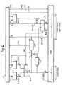
- Figure 4 shows diagrammatically certain logic elements in the processing unit of the apparatus in Figures 1 to 3.
- In the following description of the apparatus which is exemplified in the drawings, it will be assumed that memory is connected to the processing unit as a plurality of memory units each of the same number of storage bytes, this number corresponding to the smallest size of memory unit which is envisaged. Such a smallest size of memory unit will be deemed to be a "chapter" of memory for the purposes of the present description. These memory units can be respective memory devices each containing one "chapter" of memory, or a larger size memory device can be considered as a plurality of memory units each containing one "chapter" of memory. Each such larger size memory device would always contain an integral number of "chapters" of memory. Thus, a "chapter" can be 1024 bytes of 8 bits, and, as will be described with reference to Figures 1 to 3, Random Access Memory (RAM) devices of 1, 2 and 4 chapter sizes could be available for use.
- Referring now to the drawings, the digital apparatus shown in each of Figures 1 to 3 comprises an integrated circuit IC containing a processing unit PU and an interface circuit INTF which are interconnected internally in the integrated circuit IC. The integrated circuit IC has sixteen external connecting pins CP1 to CP16 by which external connection is made to RAM equipment RM which contains different numbers and configurations of memory units in the three Figures, as will be described. (The integrated circuit IC would, of course, have further external connecting pins (not shown) for applying thereto supply voltages, and for clock and control signals, etc.).
- A 6-line address bus consisting of parallel address lines CA1 to CA6 extends between the RAM equipment RM and the connecting pins CP1 to CP6. Binary 6-bit chapter address codes applied from the processing unit PU over this address bus will select certain of the memory units in the RAM equipment RM. These 6-bit address codes constitute valid or invalid address codes, respectively, according as they can select only one, or more than one, memory unit.
- A 10-line address bus connected to connecting pins CP7 to CP16 and consisting of parallel address lines BA1 to BA10, carries binary 10-bit byte address codes for identifying the 1024 8-bit bytes contained in each memory unit. This identification can be effected in known manner using a decoder (not shown) for converting the 10-bit address codes into suitable "byte" select signals. Of the address lines BA1 to BA10, the first eight (BA1 to BA8) also serve as data lines DT1 to DT8 which form an 8-line data bus for the transfer of data between the integrated circuit IC and the RAM equipment RM. The direction of data transfer is controlled from the processing unit PU. The address/data bus (BA1 to BA10, DT1 to DT8) is used on a multiplex basis in different time intervals for either byte addressing or data transfer, this multiplexing also being controlled from the processing unit PU. As an alternative, a separate 8-line data bus can be provided, but this requires an additional eight connecting pins on the integrated circuit IC.
- In Figure 1, the RAM equipment RM comprises six discrete RAM devices RM1(1) to RM6(1) each of which has a capacity of one memory unit. Each of the devices RM1(1) to RM6(1) has a so-called "chip" select terminal TCS, and the address lines CA1 to CA6 are connected respectively to these terminals. When one of these address lines is made active (e.g. active high to signify binary level "1") by the processing unit PU to constitute a "chip" select signal, the particular RAM device to which that address line is connected is selected for data transfer. Byte addressing and data transfer can thereafter be effected over the address/data lines BA1 to BA10/DT1 to DT8.
- Details of circuits which are used for "chip" selecting, byte addressing and data transfer are readily available and will not, therefore, be described in the present specification in respect of the apparatus shown in Figures 1 to 3; particularly also as a description of such circuit details is not necessary for an understanding of the present invention.
- The RAM equipment RM of the apparatus shown in Figure 2 comprises five discrete RAM devices RM1(2) to RM5(2) each of which has a capacity of two memory units. In this apparatus, the address lines CA1 to CA5 are connected to the "chip" select terminal of the respective RAM devices, while the address line CA6 is connected to a 1-out-of-2 "unit" select terminal UST of each device and is used to determine which of the two memory units of a selected RAM device is to be chosen, according as this latter address line CA6 is made active high (binary level "1") or active low (binary level "0").
- The RAM equipment RM of the apparatus shown in Figure 3 comprises four discrete RAM devices RM1(4) to RM4(4) each of which has a capacity of four memory units. The address lines CA1 to CA4 are connected to the "chip" select terminal TCS of the respective RAM devices, while the address lines CA5 and CA6 are connected respectively to 1-out-of-4 "unit" select terminals UST1 and UST2 of each device and are used to determine, in accordance with their unique binary level combinations (00, 01, 10 and 11), which one of the four memory units of a selected RAM device is to be chosen.
- For the memory unit choice in Figure 2, simple gating logic would be provided in the RAM devices to distinguish between the "1" and "0" binary levels of the address line CA6, while for the memory unit choice in Figure 3, a simple decoder would be provided in the RAM devices to select the four different "1" and "0" binary level combinations of the address lines CA5 and CA6.
- It will be appreciated from the foregoing examples of specific digital data apparatus of the character referred to, as shown in Figures 1 to 3, that for a given number n of address lines which are provided for chapter address codes, (n-m) of these n address lines can be used directly for addressing discrete RAM devices each containing 2m chapter size memory units, where m equals 0, 1, 2,... (n-1) with simple decoding for determining the 2"' different combinations when /?r>0.
- As shown in Figure 4, the processing unit PU includes a chapter addresser C/ADD for producing the 6-bit chapter address codes for application via a 6-bit connection CY/AD to the address bus CA1 to CA6 by way of a multiplexer MUX1 in its unswitched state. A logic circuit LC of the processing unit controls the operation of the chapter addresser C/ADD over a control lead or leads CAC. A possible means-of implementation and control would be for the logic circuit LC to supply stepping pulses to a counter, which forms the chapter addresser, until a count corresponding to a required address code is reached, following which this address code would be held latched for application to the address bus. Additionally, these 6-bit address codes are produced periodically in a special sequence by a chapter address sequencer C/SEQ in response to a control signal from the logic circuit LC on a control lead SAC. In this instance also a convenient means of implementation and control would be for the logic circuit LC to supply stepping pulses to a counter which forms the chapter address sequencer, but with the counter having its counting stages interconnected with appropriate gating and feed-back paths to produce a count according to the special sequence instead of its natural count. The sequenced address codes are applied to the address bus CA1 to CA6 by way of the multiplexer MUX1 in its switched state, the switching of this multiplexer being effected by the control signal on the control lead SAC.
- The sequenced address codes, along with flag bits as will be described, are also applied by way of another multiplexer MUX2, in its switched state, to the data bus DT1 to DT8 to be recorded with the flag bits as identification codes in a specially allocated storage location (byte) in each of those memory units which are provided. The specially allocated storage location is the same byte in each memory unit and is identified, both for writing into and for reading from, by the appropriate byte address code as produced by a byte addresser B/ADD, which produces the 10-bit byte address codes on a 10-bit connection BY/AD for application to the address bus BA1 to BA10, in response to a RAM finder signal from the logic circuit LC on a control lead RF. The logic circuit LC otherwise controls the byte addresser B/ADD for byte addressing during normal memory unit operation over a control lead BAC. Also, for normal memory unit operation, data written into a memory unit storage byte is fed from the logic circuit LC by way of the multiplexer MUX2, in its unswitched state, over an 8-bit connection DAT/OT to the data bus DT1 to DT8: data read from a memory unit storage byte is fed to the logic circuit LC from the data bus DT1 to DT8 over an 8-bit connection DAT/IN. The leads RD, WR and ALE signify the "read", "write" and "address latch enable" control which is exercised in conventional known manner by the logic circuit LC on the memory units.
- The processing unit PU also includes a comparator COMP and a flag bit producer FLG. The chapter address codes at the output of the multiplexer MUX1 are applied to both the comparator COMP and to the flag bit producer FLG, which latter is responsive to an applied chapter address code to produce two flag bits the binary value combination of which is representative of how many bits of the value which constitutes a "chip" select signal are contained in the address code. These two flag bits are applied to the comparator COMP along with the 6-bit chapter address code. The 6-bit chapter address codes, along with their respective two flag bits, also form the 8-bit identification codes which are applied over the data bus DT1 to DT8 for recording in the specially allocated storage location in the memory units. A chapter address code applied to the address bus CA1 to CA6 is tested for validity by the comparator COMP by comparing this address code with the corresponding 6-bit portion of the identification code which is read from the specially allocated storage location of the memory unit which is (notionally) being addressed by the chapter address code being tested. If this comparison shows agreement then the test for validity as set forth in our said co-pending U.K. Patent Application is satisfied.
- In accordance with the present invention the comparison which is effected by the comparator COMP also extends to the flag bits to test the validity of a chapter address code in respect of its ability to select one and only one memory unit. If this second test for validity, which will be considered in detail next, is satisfied then the comparator COMP produces a chapter valid signal on a lead CVS, and the logic circuit knows that for the chapter address code concerned, a memory unit has been provided in which data can be stored.
- When a special writing sequence is to be carried out to record identification codes in the specially allocated storage locations of those memory units which are provided, the logic circuit LC applies a control signal to the control lead RF to cause the byte addresser B/ADD to produce the address of the specially allocated storage location, and it applies a control signal to the control lead SAC to switch the multiplexers MUX1 and MUX2 and to start the chapter address sequencer C/SEQ. This special writing sequence, which would be initiated when power to the apparatus is switched on, and/or at relatively infrequent intervals when the apparatus is in use, goes through all the possible chapter address codes in the order defined in Table I below, and each address code as it is produced to select a memory unit is written into the specially allocated storage location of the memory unit, together with certain flag bits. (The Table I assumes binary "1" as active chip select).


- This sequence in Table II, which occurs as a result of the special writing sequence according to Table I, comprises all the chapter address codes which have the value "1" in the (least significant) bit position which pertains to the RAM device RM6(1 Similarly, the RAM device RM5(1) would have chapter address codes written into its special storage location in a sequence such as set forth in Table III below, each code again over-writing the previous code, so that 000010 remains as the address code which is finally recorded as part of the identification code.

- The other RAM devices RM4(1), RM3(1), RM2(1 ) and RM1(1) are treated similarly so that address codes 000100,001000,010000 and 100000 are recorded in their respective specially allocated storage locations as part of their identification codes.
- As regards the apparatus in Figure 2, it will be evident from the foregoing that chapter address codes 000010 and 000011 will both "chip select" the RAM device RM5(2), with these two codes respectively pertaining to the two memory units of this device and therefore being recorded in the specially allocated storage location of the appertaining memory unit as part of its identification code. Similarly, the pairs of chapter address codes 000100, 000101; 001000, 001001; 010000, 010001; and 100000, 100001 pertain respectively to the two memory units in the other four RAM devices RM4(2) to RM1(2).
- As regards the apparatus in Figure 3, it will further be evident that each of the four chapter address codes 000100, 000101, 000110 and 000111 will "chip select" the RAM device RM4(4), with these four codes respectively pertaining to the four memory units of this device and therefore being recorded in the specially allocated storage location of the appertaining memory unit as part of its identification code. Similarly, the sets of four chapter address codes 001000, 001001, 001011; 010000, 010001, 010010, 010011; and 100000, 100001, 100010, 100011 pertain respectively to the four memory units in the other three RAM devices RM3(4), RM2(4) and RM1(4).
- The configurations of digital data apparatus shown in Figures 1 to 3 are just examples of the many configurations which are possible, and within each configuration the total possible number of memory units need not be provided. Within these confines, the special writing sequence as set forth above in Table I ensures that the chapter address code recorded as part of the identification code in each memory unit which is provided is unique to that memory unit. Also, within the above confines, the processing unit of the digital data apparatus has to be able to select a memory unit for use simply by applying chapter address codes to the address bus in, say, a natural binary counting sequence, until a single memory unit is selected for use. As mentioned previously, the flag bits which are included in the identification codes recorded in the specially allocated storage locations of the memory units provide a means for invalidating those chapter address codes which select more than one memory unit. These flag bits, of which in the present embodiment there are two in each identification code, signify the number of binary bits of "1" value contained in the code. All the chapter address codes having the same number of "1"s (and thus "0"s) have the same two flag bits allocated to them, both as part of the identification codes for the memory units, and for the comparison operation performed by the comparator COMP in Figure 4 between the chapter address code which is addressing the memory units and the identification code(s) resulting from this addressing. Suitable flag bit combinations are 11, 10 and 01 for one, two and three 1's respectively, in an address code, and the flag bit combination 00 is used for none, four, five and six 1's in an address code.
- Consider now some examples, in the configuration of apparatus shown in Figure 1, the chapter address code 000000 will select none of the RAM devices RM1 (1) to RM6(1) so that the comparator COMP (Figure 4), which receives 000000 00 as the code plus flag bits, receives no resulting identification code and therefore does not produce the chapter valid signal on lead CVS. When a chapter address code having a single "1" in it (e.g. 000001 plus flag bits 11) is produced by the processing unit, only one RAM device (i.e. RM6(1) for code 000001 if actually provided) is selected and thus outputs the identification code with the matching address code and flag bits. The comparator COMP agrees the comparison to produce the chapter valid signal on the lead CVS. With a chapter address code containing two 1's (and four O's), e.g. 000011
plus flag bits 10, two RAM devices (i.e. RM6(1) and RM5(1)) are selected simultaneously. This produces conflicts on the six data lines of the data bus DT1 to DT8 which carry the address code part of the identification codes, this data conflict preventing the comparator COMP from effecting a proper comparison of this part with the applied address code. However, both of the RAM devices output the same two flag bits (11), and so those two bits are not in conflict on the other two data lines of the data bus. These two flag bits (11) do not match the two flag bits (10) which are allocated to the address code 000011 and the comparator COMP therefore rejects this address code as invalid. - With a chapter address code containing three 1's and three 0's, the relevant three of the RAM devices RM1 (1) to RM6(1) are selected, again resulting in data conflict on three of the six lines of the data bus which carry the address code part of the identification codes. However, once again the flag bits (01) do not match the common flag bits (11) in the three identification codes concerned, so that once again the comparator COMP rejects this address code as invalid. It will be apparent that address codes containing four, five and six 1's are similarly rejected as being invalid.
- In the specific examples of digital data apparatus shown in Figures 1 to 3, the memory units are assumed to be organized in 8-bit bytes, as discussed above. Therefore, using the 6-bit address codes as part of the identification codes leaves only two bits for the flag bits, so that only four types of chapter address codes can be distinguished, i.e. those containing one 1, two 1's, three 1's and others, as required by these specific examples. The logic operation of these three specific examples is given in the following Tables IV, V and VI, respectively.


- It can be seen from Table IV that, as given in the earlier examples, valid chapter address codes contain only a single 1 for the apparatus of Figure 1. From Table V it can be seen that valid chapter address codes contain one or two 1's for the apparatus of Figure 2, and from Table VI that they contain one, two or three 1's for the apparatus of Figure 3. For the apparatus of Figure 1, only valid chapter address codes contain a single 1. For the apparatus of Figure 2, both valid and invalid chapter address codes can contain one or two 1's, but such invalid chapter address codes are identified as being invalid because their associated flag bits are different from the flag bits in the identification codes of the memory units which they address. For example, the invalid address code 000110 (with flag bits 10) is equivalent to the two address codes 000100 and 000010 (each with flag bits 11) which are in the identification codes that are produced by this invalid address code for comparison. The address code part of those identification codes is therefore different and thus causes data bus conflicts, as aforesaid. The flag bits (11) are the same for each code and are different from the flag bits (10) associated with the applied chapter address code. Therefore, this address code is detected as being invalid, as required.
- For the apparatus of Figure 3, both valid and invalid chapter address codes can contain one, two or three 1 's, but again the difference in the flag bits distinguishes between the valid and invalid address codes. For example, the invalid address code 001110 (with flag bits 01) is equivalent to the two address codes 001010 and 000110 (each with flag bits (10) which are in the identification codes that are produced by this invalid address code for comparison. The address code part of these identification codes is therefore different and thus causes data bus conflicts. The flag bits (10) are the same for each code and are different from the flag bits (01) associated with the applied chapter address code. Therefore, this address code is rejected as being invalid.
- In the Tables IV, V and VI, "etc." implies (as it does in Table I) the other code combinations with the pattern concerned. For instance, in Table VI, "000101/000110 etc." implies the code combinations "001001/001010", "010001/010010" and "100001/1000010", all of which code combinations pertain respectively to two of the valid chapter address codes for the RAM devices RM4(1) to RM1(4).
- The principle of the invention can be extended to other configurations of digital data apparatus, for instance to three "chip selected" RAM devices each comprising eight chapter size memory units. Such a configuration could be catered for by allocating another special storage location in each memory unit for identification purposes to increase the number of flag bits that can be included in the identification codes. Also, the use of chapter address codes with a different number of bits is possible. For example, five bit chapter address codes can define 1 to 32 memory units, leaving 3 bits in an 8-bit byte for flag bits which are sufficient to define all 6 different code combinations for the address codes; that is, code combinations having 0, 1, 2, 3, 4 and 5 ones. An apparatus configuration comprising two RAM devices each containing eight memory units will be catered for in this way by using two of the address lines to "chip select" the RAM devices and the other three address lines to define the eight memory units of a RAM device.
Claims (6)
Applications Claiming Priority (2)
| Application Number | Priority Date | Filing Date | Title |
|---|---|---|---|
| GB08123483A GB2103397A (en) | 1981-07-31 | 1981-07-31 | Digital data aparatus with memory selection |
| GB8123483 | 1981-07-31 |
Publications (3)
| Publication Number | Publication Date |
|---|---|
| EP0071315A2 EP0071315A2 (en) | 1983-02-09 |
| EP0071315A3 EP0071315A3 (en) | 1986-01-15 |
| EP0071315B1 true EP0071315B1 (en) | 1990-01-03 |
Family
ID=10523602
Family Applications (1)
| Application Number | Title | Priority Date | Filing Date |
|---|---|---|---|
| EP82200940A Expired - Lifetime EP0071315B1 (en) | 1981-07-31 | 1982-07-22 | Digital data apparatus with peripheral unit select |
Country Status (7)
| Country | Link |
|---|---|
| US (1) | US4481579A (en) |
| EP (1) | EP0071315B1 (en) |
| JP (1) | JPS5827225A (en) |
| AU (1) | AU547280B2 (en) |
| CA (1) | CA1193749A (en) |
| DE (1) | DE3280077D1 (en) |
| GB (1) | GB2103397A (en) |
Families Citing this family (20)
| Publication number | Priority date | Publication date | Assignee | Title |
|---|---|---|---|---|
| JPS5960786A (en) * | 1982-09-30 | 1984-04-06 | Fujitsu Ltd | semiconductor integrated circuit |
| US4740916A (en) * | 1985-12-19 | 1988-04-26 | International Business Machines Corporation | Reconfigurable contiguous address space memory system including serially connected variable capacity memory modules and a split address bus |
| US5056060A (en) * | 1987-03-13 | 1991-10-08 | Apple Computer, Inc. | Printed circuit card with self-configuring memory system for non-contentious allocation of reserved memory space among expansion cards |
| IL85518A0 (en) * | 1987-03-13 | 1988-08-31 | Apple Computer | Computer with expansion slots for cards and card therefor |
| US4905182A (en) * | 1987-03-13 | 1990-02-27 | Apple Computer, Inc. | Self-configuring memory management system with on card circuitry for non-contentious allocation of reserved memory space among expansion cards |
| US4931923A (en) * | 1987-03-13 | 1990-06-05 | Apple Computer, Inc. | Computer system for automatically reconfigurating memory space to avoid overlaps of memory reserved for expansion slots |
| EP0393290B1 (en) * | 1989-04-19 | 1995-08-16 | International Business Machines Corporation | Memory and peripheral chip select apparatus |
| US5195100A (en) * | 1990-03-02 | 1993-03-16 | Micro Technology, Inc. | Non-volatile memory storage of write operation identifier in data sotrage device |
| US5233618A (en) * | 1990-03-02 | 1993-08-03 | Micro Technology, Inc. | Data correcting applicable to redundant arrays of independent disks |
| JPH05108484A (en) * | 1990-06-07 | 1993-04-30 | Intel Corp | Cache memory |
| US5276838A (en) * | 1991-03-04 | 1994-01-04 | International Business Machines Corporation | Dynamically repositioned memory bank queues |
| US5430859A (en) * | 1991-07-26 | 1995-07-04 | Sundisk Corporation | Solid state memory system including plural memory chips and a serialized bus |
| US5455919A (en) * | 1992-11-03 | 1995-10-03 | International Business Machines Corporation | Installation and use of plural expanded memory managers |
| US5611054A (en) * | 1994-03-18 | 1997-03-11 | Intel Corporation | Method and apparatus for decoding and recoding of addresses |
| GB2288953B (en) * | 1994-03-21 | 1998-08-05 | Peter Wolstenholme | Self-testing secure-transaction computer input-output bus |
| US5842025A (en) * | 1996-08-27 | 1998-11-24 | Mmc Networks, Inc. | Arbitration methods and apparatus |
| EP0886824A1 (en) * | 1996-12-13 | 1998-12-30 | Nyquist B.V. | Redundant data processing system having two programmed logic controllers operating in tandem |
| KR100669256B1 (en) | 2005-05-23 | 2007-01-16 | 주식회사 화인테크닉스 | Powder quantitative feeder, raw material supply device and powder quantitative feeding method |
| US9201790B2 (en) * | 2007-10-09 | 2015-12-01 | Seagate Technology Llc | System and method of matching data rates |
| US8060658B2 (en) * | 2008-03-06 | 2011-11-15 | Siemens Industry, Inc. | Auto addressing devices on a common power and communication bus structure and method therefor |
Family Cites Families (12)
| Publication number | Priority date | Publication date | Assignee | Title |
|---|---|---|---|---|
| US4135240A (en) * | 1973-07-09 | 1979-01-16 | Bell Telephone Laboratories, Incorporated | Protection of data file contents |
| US4263650B1 (en) * | 1974-10-30 | 1994-11-29 | Motorola Inc | Digital data processing system with interface adaptor having programmable monitorable control register therein |
| US3967251A (en) * | 1975-04-17 | 1976-06-29 | Xerox Corporation | User variable computer memory module |
| US4041472A (en) * | 1976-04-29 | 1977-08-09 | Ncr Corporation | Data processing internal communications system having plural time-shared intercommunication buses and inter-bus communication means |
| US4200930A (en) * | 1977-05-23 | 1980-04-29 | Burroughs Corporation | Adapter cluster module for data communications subsystem |
| US4158227A (en) * | 1977-10-12 | 1979-06-12 | Bunker Ramo Corporation | Paged memory mapping with elimination of recurrent decoding |
| US4195351A (en) * | 1978-01-27 | 1980-03-25 | International Business Machines Corporation | Loop configured data transmission system |
| US4164786A (en) * | 1978-04-11 | 1979-08-14 | The Bendix Corporation | Apparatus for expanding memory size and direct memory addressing capabilities of digital computer means |
| GB2060961A (en) * | 1979-10-10 | 1981-05-07 | Magnuson Computer Systems Inc | Data processing system having memory modules with distributed address information |
| US4326250A (en) * | 1979-10-10 | 1982-04-20 | Magnuson Computer Systems, Inc. | Data processing apparatus with serial and parallel priority |
| US4321667A (en) * | 1979-10-31 | 1982-03-23 | International Business Machines Corp. | Add-on programs with code verification and control |
| US4335426A (en) * | 1980-03-10 | 1982-06-15 | International Business Machines Corporation | Remote processor initialization in a multi-station peer-to-peer intercommunication system |
-
1981
- 1981-07-31 GB GB08123483A patent/GB2103397A/en not_active Withdrawn
-
1982
- 1982-07-12 US US06/397,389 patent/US4481579A/en not_active Expired - Fee Related
- 1982-07-22 EP EP82200940A patent/EP0071315B1/en not_active Expired - Lifetime
- 1982-07-22 DE DE8282200940T patent/DE3280077D1/en not_active Expired - Lifetime
- 1982-07-29 CA CA000408438A patent/CA1193749A/en not_active Expired
- 1982-07-30 AU AU86602/82A patent/AU547280B2/en not_active Ceased
- 1982-07-31 JP JP57133003A patent/JPS5827225A/en active Granted
Non-Patent Citations (3)
| Title |
|---|
| EDN Magazine, vol 26 (1981), Febr., No 3, page 88 * |
| IBM Technical Disclosure Bulletin, Vol 18. No 3, August 1975, pages 878, 879 * |
| Proceedings of the IRE, Jan. 1961, pages 53 and 54 * |
Also Published As
| Publication number | Publication date |
|---|---|
| JPS5827225A (en) | 1983-02-17 |
| US4481579A (en) | 1984-11-06 |
| JPH0243213B2 (en) | 1990-09-27 |
| EP0071315A2 (en) | 1983-02-09 |
| EP0071315A3 (en) | 1986-01-15 |
| AU8660282A (en) | 1983-02-03 |
| CA1193749A (en) | 1985-09-17 |
| GB2103397A (en) | 1983-02-16 |
| AU547280B2 (en) | 1985-10-10 |
| DE3280077D1 (en) | 1990-02-08 |
Similar Documents
| Publication | Publication Date | Title |
|---|---|---|
| US4481579A (en) | Digital data apparatus having a plurality of selectively addressable peripheral units | |
| EP0068569B1 (en) | Digital data apparatus with memory identification | |
| EP0108346B1 (en) | Memory reconfiguration method in a data processing system | |
| EP0518367B1 (en) | System for determining pluggable memory characteristics | |
| US5727207A (en) | Method and apparatus for automatically loading configuration data on reset into a host adapter integrated circuit | |
| EP0473275B1 (en) | Memory control unit and memory unit | |
| US5237567A (en) | Processor communication bus | |
| US4814982A (en) | Reconfigurable, multiprocessor system with protected, multiple, memories | |
| US5129069A (en) | Method and apparatus for automatic memory configuration by a computer | |
| US4787060A (en) | Technique for determining maximum physical memory present in a system and for detecting attempts to access nonexistent memory | |
| EP0226791A2 (en) | A memory with means for allocating address space among modules | |
| EP0449661A2 (en) | Computer for Simultaneously executing plural instructions | |
| US4744025A (en) | Arrangement for expanding memory capacity | |
| US4271521A (en) | Address parity check system | |
| US5179686A (en) | Method for automatically detecting the size of a memory by performing a memory warp operation | |
| US4785452A (en) | Error detection using variable field parity checking | |
| GB2215497A (en) | Self configuring memory system | |
| EP0136178A2 (en) | Automatic memory board reconfiguration | |
| US5003506A (en) | Memory capacity detection apparatus and electronic applied measuring device employing the same | |
| US4696005A (en) | Apparatus for reducing test data storage requirements for high speed VLSI circuit testing | |
| US4958323A (en) | Semiconductor file memory | |
| EP0200198B1 (en) | An arrangement for expanding memory capacity | |
| JPS5848944B2 (en) | processing equipment | |
| CA1269177A (en) | System for maintaining the hardware-software compatibility of modular communication systems | |
| EP0173746A1 (en) | System of selecting address in input/output board |
Legal Events
| Date | Code | Title | Description |
|---|---|---|---|
| PUAI | Public reference made under article 153(3) epc to a published international application that has entered the european phase |
Free format text: ORIGINAL CODE: 0009012 |
|
| 17P | Request for examination filed |
Effective date: 19820722 |
|
| AK | Designated contracting states |
Designated state(s): DE FR GB IT SE |
|
| PUAL | Search report despatched |
Free format text: ORIGINAL CODE: 0009013 |
|
| AK | Designated contracting states |
Designated state(s): DE FR GB IT SE |
|
| 17Q | First examination report despatched |
Effective date: 19880428 |
|
| RAP3 | Party data changed (applicant data changed or rights of an application transferred) |
Owner name: N.V. PHILIPS' GLOEILAMPENFABRIEKEN Owner name: PHILIPS ELECTRONIC AND ASSOCIATED INDUSTRIES LIMIT |
|
| GRAA | (expected) grant |
Free format text: ORIGINAL CODE: 0009210 |
|
| AK | Designated contracting states |
Kind code of ref document: B1 Designated state(s): DE FR GB IT SE |
|
| REF | Corresponds to: |
Ref document number: 3280077 Country of ref document: DE Date of ref document: 19900208 |
|
| ITF | It: translation for a ep patent filed | ||
| ET | Fr: translation filed | ||
| PGFP | Annual fee paid to national office [announced via postgrant information from national office to epo] |
Ref country code: GB Payment date: 19900702 Year of fee payment: 9 |
|
| PGFP | Annual fee paid to national office [announced via postgrant information from national office to epo] |
Ref country code: FR Payment date: 19900720 Year of fee payment: 9 |
|
| PGFP | Annual fee paid to national office [announced via postgrant information from national office to epo] |
Ref country code: SE Payment date: 19900726 Year of fee payment: 9 |
|
| ITTA | It: last paid annual fee | ||
| PGFP | Annual fee paid to national office [announced via postgrant information from national office to epo] |
Ref country code: DE Payment date: 19900921 Year of fee payment: 9 |
|
| PLBE | No opposition filed within time limit |
Free format text: ORIGINAL CODE: 0009261 |
|
| STAA | Information on the status of an ep patent application or granted ep patent |
Free format text: STATUS: NO OPPOSITION FILED WITHIN TIME LIMIT |
|
| 26N | No opposition filed | ||
| PG25 | Lapsed in a contracting state [announced via postgrant information from national office to epo] |
Ref country code: GB Effective date: 19910722 |
|
| PG25 | Lapsed in a contracting state [announced via postgrant information from national office to epo] |
Ref country code: SE Effective date: 19910723 |
|
| GBPC | Gb: european patent ceased through non-payment of renewal fee | ||
| PG25 | Lapsed in a contracting state [announced via postgrant information from national office to epo] |
Ref country code: FR Effective date: 19920331 |
|
| PG25 | Lapsed in a contracting state [announced via postgrant information from national office to epo] |
Ref country code: DE Effective date: 19920401 |
|
| REG | Reference to a national code |
Ref country code: FR Ref legal event code: ST |
|
| EUG | Se: european patent has lapsed |
Ref document number: 82200940.3 Effective date: 19920210 |