EP0071284B1 - Energy converter - Google Patents
Energy converter Download PDFInfo
- Publication number
- EP0071284B1 EP0071284B1 EP82200835A EP82200835A EP0071284B1 EP 0071284 B1 EP0071284 B1 EP 0071284B1 EP 82200835 A EP82200835 A EP 82200835A EP 82200835 A EP82200835 A EP 82200835A EP 0071284 B1 EP0071284 B1 EP 0071284B1
- Authority
- EP
- European Patent Office
- Prior art keywords
- energy
- circuit
- current
- series
- voltage
- Prior art date
- Legal status (The legal status is an assumption and is not a legal conclusion. Google has not performed a legal analysis and makes no representation as to the accuracy of the status listed.)
- Expired
Links
Images

Classifications
-
- H—ELECTRICITY
- H02—GENERATION; CONVERSION OR DISTRIBUTION OF ELECTRIC POWER
- H02M—APPARATUS FOR CONVERSION BETWEEN AC AND AC, BETWEEN AC AND DC, OR BETWEEN DC AND DC, AND FOR USE WITH MAINS OR SIMILAR POWER SUPPLY SYSTEMS; CONVERSION OF DC OR AC INPUT POWER INTO SURGE OUTPUT POWER; CONTROL OR REGULATION THEREOF
- H02M3/00—Conversion of DC power input into DC power output
- H02M3/22—Conversion of DC power input into DC power output with intermediate conversion into AC
- H02M3/24—Conversion of DC power input into DC power output with intermediate conversion into AC by static converters
- H02M3/28—Conversion of DC power input into DC power output with intermediate conversion into AC by static converters using discharge tubes with control electrode or semiconductor devices with control electrode to produce the intermediate AC
- H02M3/305—Conversion of DC power input into DC power output with intermediate conversion into AC by static converters using discharge tubes with control electrode or semiconductor devices with control electrode to produce the intermediate AC using devices of a thyratron or thyristor type requiring extinguishing means
- H02M3/315—Conversion of DC power input into DC power output with intermediate conversion into AC by static converters using discharge tubes with control electrode or semiconductor devices with control electrode to produce the intermediate AC using devices of a thyratron or thyristor type requiring extinguishing means using semiconductor devices only
- H02M3/3155—Conversion of DC power input into DC power output with intermediate conversion into AC by static converters using discharge tubes with control electrode or semiconductor devices with control electrode to produce the intermediate AC using devices of a thyratron or thyristor type requiring extinguishing means using semiconductor devices only with automatic control of the output voltage or current
Definitions
- the energy supplied to the buffer may be returned to the source or extracted by the load.
- the energy balance setting is determined by the times at which the thyristors of the bridge circuit are triggered.
- An energy converter of the above type is disclosed, for example, in the U.S. Patent No. 3,953,779.
- the energy converter comprises an analogue control circuit. This circuit responds, among others, to a voltage derived from the output voltage of the output transformer and delivers trigger pulses to bring the appropriate thyristors into the conducting state.
- the trigger frequency of the thyristors changes.
- the invention thereto provides an energy converter comprising a number of energy transfer units accommodated in parallel in the series-resonant circuit for feeding loads to be connected separately thereto, each of said energy transfer units being provided with an output transformer incorporated in the series-resonant circuit, an energy buffer coupled to the secondary winding of the relevant output transformer for supply of energy to a load to be connected thereto, and a control circuit of a first type activated by the voltage across the relevant energy buffer for the control of the current through the primary winding of the relevant output transformer for the maintenance of a constant voltage across the corresponding energy buffer; whereby the series-resonant circuit comprises a single control unit of a second type accommodated in the series-resonant circuit in parallel with the energy transfer units and provided with a transformer incorporated in the series-resonant circuit, the secondary winding of the latter transformer being connected to the input poles of the bridge circuit via a rectifier circuit; and whereby the bridge circuit is adjustable on a fixed switching frequency.
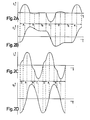
- Fig. 2A shows the current i L flowing through coil 11 and Fig. 2B the voltage E c across points P and Q.
- phase A thyristor phase
- the current i L increases in the first instance and causes the voltage E c to rise, whereupon current i L decreases to zero; the voltage E c then reaches its maximum value.
- phase B diode phase
- the voltage E c decreases slightly because of the reverse current.
- Energy transfer units 21 and 22 comprise a conversion circuit 23 and 24 respectively, and a current control unit.
- the current control units consist of transducers 25 and 26.
- the conversion circuits 23 and 24 are used to derive from the voltage across energy buffers 6 and 7 a control current for transducers 25 and 26. With this control current a pulse width control of the current through the primary winding of output transformers 2 and 3 is achieved.
- Thyristor pairs 13, 16 and 14, 15 are triggered at a fixed frequency.
- the thyristor pair to be triggered and the time of triggering are controlled by the timing and memory unit 31.
- the thyristor trigger circuit 30 On receipt of the signals for the thyristor triggering from the timing and memory unit 31, the thyristor trigger circuit 30 generates the trigger pulses for the thyristors to be brought into the conducting state.
- the trigger pulses for thyristors 14 and 15 may not be supplied until thyristors 13 and 16 are blocked.
- the thyristors are blocked when the diodes, connected antiparallel thereto, start conducting.
- the conducting state of the diodes is established by the diode current detection circuit. This circuit therefore supplies signals functioning as a condition for the release of signals to the trigger circuit 30 by the timing and memory unit 31.
Landscapes
- Engineering & Computer Science (AREA)
- Power Engineering (AREA)
- Ac-Ac Conversion (AREA)
- Rectifiers (AREA)
- Dc-Dc Converters (AREA)
Description
- The invention relates to an energy converter as specified in the precharacterising part of
claim 1 and can be used for converting electrical energy from a single phase or a polyphase AC source or from a DC source to electrical energy with a single phase or a polyphase AC voltage of a different amplitude and/or frequency, with a pulsating voltage, or with a DC voltage. Energy converters ideally suited for this purpose are of the type utilising a bridge circuit provided with at least two thyristors and a series-resonant circuit. With the relevant thyristors of the bridge circuit in the conducting state, energy from the source is supplied to the energy buffer via the series resonant circuit, and energy is extracted from the buffer by the load. During the time the thyristors are not in the conducting state, the energy supplied to the buffer may be returned to the source or extracted by the load. The energy balance setting is determined by the times at which the thyristors of the bridge circuit are triggered. An energy converter of the above type is disclosed, for example, in the U.S. Patent No. 3,953,779. In this patent specification the energy converter comprises an analogue control circuit. This circuit responds, among others, to a voltage derived from the output voltage of the output transformer and delivers trigger pulses to bring the appropriate thyristors into the conducting state. Depending on the current drawn by the load, that is depending on the voltage across the energy buffer, the trigger frequency of the thyristors changes. Such a control voltage is not applicable, however, in the event several loads are to draw current from the bridge circuit. The present invention has for its object to provide an energy converter of the type referred to above to obviate the disadvantages incurred with the absence of a trigger timing for the thyristors. - The invention thereto provides an energy converter comprising a number of energy transfer units accommodated in parallel in the series-resonant circuit for feeding loads to be connected separately thereto, each of said energy transfer units being provided with an output transformer incorporated in the series-resonant circuit, an energy buffer coupled to the secondary winding of the relevant output transformer for supply of energy to a load to be connected thereto, and a control circuit of a first type activated by the voltage across the relevant energy buffer for the control of the current through the primary winding of the relevant output transformer for the maintenance of a constant voltage across the corresponding energy buffer; whereby the series-resonant circuit comprises a single control unit of a second type accommodated in the series-resonant circuit in parallel with the energy transfer units and provided with a transformer incorporated in the series-resonant circuit, the secondary winding of the latter transformer being connected to the input poles of the bridge circuit via a rectifier circuit; and whereby the bridge circuit is adjustable on a fixed switching frequency.
- The trigger frequency of the thyristors is constant and is, unlike before, independent of the voltage across the energy buffer. For each of the energy buffers the energy balance is set separately by a special control circuit.
- The invention will now be described with reference to the accompanying figures, of which:
- Fig. 1 is an embodiment of the energy converter with a double load connected in parallel according to the invention;
- Figs. 2A, 2B, 2C and 2D are diagrams useful in explaining the operation of the bridge circuit; and
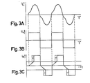
- Figs. 3A, 3B and 3C are diagrams useful in explaining the operation of the special control circuits.
- The energy converter of Fig. 1 comprises a
bridge circuit 1, parallel-connectedoutput transformers energy buffers 6 and 7. Energy from a source 8 is supplied to aload 9 via thebridge circuit 1, theoutput transformer 2, the rectifier 4 and the energy buffer 6. Energy from the source 8 is supplied to aload 10 via thebridge circuit 1, theoutput transformer 3, the rectifier 5 and theenergy buffer 7. The bridge circuit comprises a series resonant circuit consisting of acoil 11 and acapacitor 12, fourthyristors diodes - Fig. 2A shows the current iL flowing through
coil 11 and Fig. 2B the voltage Ec across points P and Q. In phase A (thyristor phase) thethyristors thyristors diodes 17 and 20. In phase B (diode phase) then entered the voltage Ec decreases slightly because of the reverse current. When this diode current is finally zero, voltage Ec remains constant untilthyristors coil 11 and Fig. 2D the voltage Ec across points P and Q for the case the thyristors are brought in the conducting phase already in the diode phases; this situation is designated the "indented mode", while that of Figs. 2A and 2B is termed the "trigger mode". - In phases A and C, energy from source 8 is supplied to
energy buffers 6 and 7, while theloads 9 and TO extract the energy from the buffers. In phases B and D a part of the energy supplied to the buffers is returned to the source via the series resonant circuit and a part is extracted byloads thyristors buffers 6 and 7 is provided with anenergy transfer unit -
Energy transfer units conversion circuit conversion circuits output transformers - Fig. 3A shows again the current iL flowing through
coil 11; this is the current supplied by the series resonant bridge circuit. Fig. 38 illustrates the voltage Uo across points Q and R. Figs. 3A and 3B illustrate how much the bridge circuit shows the character of a current source. Fig. 3C shows the variation of the current is flowing through the load windings of one of the transducers and the primary winding of a corresponding output transformer. The relevant transducer halves are so dimensioned that they are not saturated by the current is only. The control current supplied to a transducer determines the instant at which the two cores of the transducer will become saturated. When this occurs the transducer forms a low impedance for current iµ and the substantially complete voltage Uo is impressed across the primary winding of the output transformer. With an increase in the control current the saturation level will be reached sooner, causing the leading edges of the current iB in Fig. 3C to be shifted to the left. In this way, using a transducer, a pulse width control of the current through the primary winding of an output transformer is obtained and, hence, a control of the voltage across the relevant buffer. - Since the bridge circuit behaves as a current source, difficulties arise when the current to be delivered is greater than the currents together passed through the transducers in the primary winding of the particular output transformers. In such a case, the voltage across Q and R will increase. Consequently, each of the control circuits tends to cut off further the current through the primary winding of the relevant output transformer and a still larger discrepancy arises between the magnitude of the current supplied by the bridge circuit and that of the current through the primary winding of the output transformers. Such an unstable control is accountable for the cores of the particular transducers getting continuously saturated to render the control circuits inoperative.
- To avoid these difficulties, an
additional output transformer 27 is incorporated. The poles of the secondary winding of this transformer are connected to the input poles of the bridge circuit via arectifier 28. If the magnitude of the current iL supplied by the bridge circuit exceeds that of the current through the primary winding ofoutput transformers output transformer 27 andrectifier 28. Consequently, the bridge circuit no longer behaves as a current source but assumes that of a voltage source. - The embodiment of Fig. 1 finally comprises a diode
current detection circuit 29, a thyristor trigger circuit 30 and a timing andmemory unit 31. - Thyristor pairs 13, 16 and 14, 15 are triggered at a fixed frequency. The thyristor pair to be triggered and the time of triggering are controlled by the timing and
memory unit 31. On receipt of the signals for the thyristor triggering from the timing andmemory unit 31, the thyristor trigger circuit 30 generates the trigger pulses for the thyristors to be brought into the conducting state. - The diode
current detection circuit 29 supplies signals indicative of the presence of current flowing throughdiodes thyristors thyristors - Conversely, the trigger pulses for
thyristors thyristors memory unit 31.
Claims (2)
that the bridge circuit (1) is adjustable on a fixed switching frequency.
Applications Claiming Priority (2)
| Application Number | Priority Date | Filing Date | Title |
|---|---|---|---|
| NL8103475A NL8103475A (en) | 1981-07-23 | 1981-07-23 | ENERGY CONVERTER. |
| NL8103475 | 1981-07-23 |
Publications (2)
| Publication Number | Publication Date |
|---|---|
| EP0071284A1 EP0071284A1 (en) | 1983-02-09 |
| EP0071284B1 true EP0071284B1 (en) | 1986-02-05 |
Family
ID=19837835
Family Applications (1)
| Application Number | Title | Priority Date | Filing Date |
|---|---|---|---|
| EP82200835A Expired EP0071284B1 (en) | 1981-07-23 | 1982-07-05 | Energy converter |
Country Status (4)
| Country | Link |
|---|---|
| US (1) | US4495555A (en) |
| EP (1) | EP0071284B1 (en) |
| DE (1) | DE3268946D1 (en) |
| NL (1) | NL8103475A (en) |
Families Citing this family (15)
| Publication number | Priority date | Publication date | Assignee | Title |
|---|---|---|---|---|
| DE3462739D1 (en) * | 1983-05-16 | 1987-04-23 | Gen Electric | Load voltage control for resonant inverter circuits |
| US4897775A (en) * | 1986-06-16 | 1990-01-30 | Robert F. Frijouf | Control circuit for resonant converters |
| DE3682904D1 (en) * | 1986-07-03 | 1992-01-23 | Siemens Ag | SWITCHING POWER SUPPLY. |
| NL8601798A (en) * | 1986-07-10 | 1988-02-01 | Hollandse Signaalapparaten Bv | ENERGY CONVERTER. |
| NL8702115A (en) * | 1987-09-07 | 1989-04-03 | Alcatel Nederland | VOLTAGE INVERTER. |
| US4916590A (en) * | 1989-07-06 | 1990-04-10 | Spectra-Physics | Series resonant magnetic amplifier power supply |
| KR0115015Y1 (en) * | 1991-09-19 | 1998-10-01 | 이헌조 | Switching driving circuit |
| US5270914A (en) * | 1992-01-10 | 1993-12-14 | Lauw Hian K | Series resonant converter control system and method |
| US5412557A (en) * | 1992-10-14 | 1995-05-02 | Electronic Power Conditioning, Inc. | Unipolar series resonant converter |
| NL9400848A (en) * | 1994-05-25 | 1996-01-02 | Sevrien Hubert Thomas Lousberg | Serial resonant converter. |
| US5737203A (en) * | 1994-10-03 | 1998-04-07 | Delco Electronics Corp. | Controlled-K resonating transformer |
| US5508708A (en) * | 1995-05-08 | 1996-04-16 | Motorola, Inc. | Method and apparatus for location finding in a CDMA system |
| DE102004035248B4 (en) * | 2004-07-21 | 2011-08-18 | Puls GmbH, 81925 | resonant converter |
| CN105262351B (en) * | 2015-08-27 | 2019-07-19 | 许继集团有限公司 | A kind of more level driving circuits |
| EP3166217A1 (en) * | 2015-11-06 | 2017-05-10 | Excelsys Technologies Limited | Llc resonant converter having multiple transformers and a parallel inductor |
Citations (1)
| Publication number | Priority date | Publication date | Assignee | Title |
|---|---|---|---|---|
| EP0030829A2 (en) * | 1979-12-13 | 1981-06-24 | Western Electric Company, Incorporated | Converter of blocking oscillator type |
Family Cites Families (5)
| Publication number | Priority date | Publication date | Assignee | Title |
|---|---|---|---|---|
| US3343068A (en) * | 1965-06-04 | 1967-09-19 | Borg Warner | Static inverter system |
| US3893015A (en) * | 1975-01-03 | 1975-07-01 | Raytheon Co | Forced voltage sharing in series-connected power inverters |
| DE2608167C3 (en) * | 1976-02-27 | 1978-11-02 | Siemens Ag, 1000 Berlin Und 8000 Muenchen | Regulated single-ended flow converter for generating several galvanically isolated output voltages |
| DE3017606A1 (en) * | 1980-05-08 | 1981-11-12 | Licentia Patent-Verwaltungs-Gmbh, 6000 Frankfurt | Rectified constant DC voltage power supply - has AC line of first network in current transformer prim. and sec. feed full-wave rectifier |
| US4333135A (en) * | 1980-05-21 | 1982-06-01 | Schwarz Francisc C | Four quadrant AC and DC to AC and DC converter with two or more independently controlled loads |
-
1981
- 1981-07-23 NL NL8103475A patent/NL8103475A/en not_active Application Discontinuation
-
1982
- 1982-07-05 EP EP82200835A patent/EP0071284B1/en not_active Expired
- 1982-07-05 DE DE8282200835T patent/DE3268946D1/en not_active Expired
- 1982-07-14 US US06/398,175 patent/US4495555A/en not_active Expired - Lifetime
Patent Citations (1)
| Publication number | Priority date | Publication date | Assignee | Title |
|---|---|---|---|---|
| EP0030829A2 (en) * | 1979-12-13 | 1981-06-24 | Western Electric Company, Incorporated | Converter of blocking oscillator type |
Also Published As
| Publication number | Publication date |
|---|---|
| US4495555A (en) | 1985-01-22 |
| EP0071284A1 (en) | 1983-02-09 |
| NL8103475A (en) | 1983-02-16 |
| DE3268946D1 (en) | 1986-03-20 |
Similar Documents
| Publication | Publication Date | Title |
|---|---|---|
| US4495555A (en) | Energy converter | |
| AU655130B2 (en) | Inverter power supply for welding | |
| EP0602835B1 (en) | Voltage control circuits | |
| US4493017A (en) | Single drive transformer with regenerative winding for p.w.m. supply having alternately conducting power devices | |
| EP0016538A1 (en) | DC-DC converter including a high-frequency inverter, and battery charger incorporating same | |
| GB1569836A (en) | Inverter circuits | |
| EP0262812A2 (en) | Buck-boost parallel resonant converter | |
| US3515974A (en) | Dc to dc power supply with isolated control circuit | |
| GB2105933A (en) | Power conversion circuit | |
| EP0071285B1 (en) | Energy converter | |
| EP0079130A1 (en) | Reactive snubber for inductive load clamp diodes | |
| US4069449A (en) | Flyback type power supply | |
| US3953781A (en) | Controllable and quenchable rectifier circuit for high direct current values | |
| US3423665A (en) | Electronic power supplies with inverters and regulators | |
| EP0012648B1 (en) | Single-pole commutation circuit | |
| US4028610A (en) | Inverters supplying a high frequency alternating current | |
| EP0797290B1 (en) | Regulated resonant converter | |
| EP0253432B1 (en) | Energy converter | |
| US3453524A (en) | Inverter commutation circuit | |
| US4744020A (en) | Switching mode power supply | |
| EP0307057A1 (en) | Energy convertor | |
| JPS6196700A (en) | X-ray apparatus | |
| US4284934A (en) | Motor control apparatus with an improved thyristor chopper circuit | |
| US3406329A (en) | Parallel inverter with rapid response time to changes in pulse durations | |
| JP3275856B2 (en) | Power converter |
Legal Events
| Date | Code | Title | Description |
|---|---|---|---|
| PUAI | Public reference made under article 153(3) epc to a published international application that has entered the european phase |
Free format text: ORIGINAL CODE: 0009012 |
|
| AK | Designated contracting states |
Designated state(s): CH DE FR GB LI NL SE |
|
| 17P | Request for examination filed |
Effective date: 19830622 |
|
| GRAA | (expected) grant |
Free format text: ORIGINAL CODE: 0009210 |
|
| AK | Designated contracting states |
Designated state(s): CH DE FR GB LI NL SE |
|
| REF | Corresponds to: |
Ref document number: 3268946 Country of ref document: DE Date of ref document: 19860320 |
|
| ET | Fr: translation filed | ||
| PLBE | No opposition filed within time limit |
Free format text: ORIGINAL CODE: 0009261 |
|
| STAA | Information on the status of an ep patent application or granted ep patent |
Free format text: STATUS: NO OPPOSITION FILED WITHIN TIME LIMIT |
|
| 26N | No opposition filed | ||
| NLT1 | Nl: modifications of names registered in virtue of documents presented to the patent office pursuant to art. 16 a, paragraph 1 |
Owner name: HASRODE B.V. TE EINDHOVEN. |
|
| NLS | Nl: assignments of ep-patents |
Owner name: HOLLANDSE SIGNAALAPPARATEN B.V. TE HENGELO (O.). |
|
| REG | Reference to a national code |
Ref country code: GB Ref legal event code: 732 |
|
| REG | Reference to a national code |
Ref country code: FR Ref legal event code: TP Ref country code: FR Ref legal event code: CD Ref country code: FR Ref legal event code: CA |
|
| REG | Reference to a national code |
Ref country code: CH Ref legal event code: PUE Owner name: HOLLANDSE SIGNAALAPPARATEN B.V. Ref country code: CH Ref legal event code: PFA Free format text: HASRODE B.V. |
|
| EAL | Se: european patent in force in sweden |
Ref document number: 82200835.5 |
|
| PGFP | Annual fee paid to national office [announced via postgrant information from national office to epo] |
Ref country code: SE Payment date: 19970610 Year of fee payment: 16 |
|
| PGFP | Annual fee paid to national office [announced via postgrant information from national office to epo] |
Ref country code: CH Payment date: 19970617 Year of fee payment: 16 |
|
| PGFP | Annual fee paid to national office [announced via postgrant information from national office to epo] |
Ref country code: FR Payment date: 19970620 Year of fee payment: 16 |
|
| PGFP | Annual fee paid to national office [announced via postgrant information from national office to epo] |
Ref country code: GB Payment date: 19970626 Year of fee payment: 16 |
|
| PGFP | Annual fee paid to national office [announced via postgrant information from national office to epo] |
Ref country code: NL Payment date: 19970717 Year of fee payment: 16 |
|
| PGFP | Annual fee paid to national office [announced via postgrant information from national office to epo] |
Ref country code: DE Payment date: 19970718 Year of fee payment: 16 |
|
| PG25 | Lapsed in a contracting state [announced via postgrant information from national office to epo] |
Ref country code: GB Free format text: LAPSE BECAUSE OF NON-PAYMENT OF DUE FEES Effective date: 19980705 |
|
| PG25 | Lapsed in a contracting state [announced via postgrant information from national office to epo] |
Ref country code: SE Free format text: LAPSE BECAUSE OF NON-PAYMENT OF DUE FEES Effective date: 19980706 |
|
| PG25 | Lapsed in a contracting state [announced via postgrant information from national office to epo] |
Ref country code: LI Free format text: LAPSE BECAUSE OF NON-PAYMENT OF DUE FEES Effective date: 19980731 Ref country code: CH Free format text: LAPSE BECAUSE OF NON-PAYMENT OF DUE FEES Effective date: 19980731 |
|
| PG25 | Lapsed in a contracting state [announced via postgrant information from national office to epo] |
Ref country code: NL Free format text: LAPSE BECAUSE OF NON-PAYMENT OF DUE FEES Effective date: 19990201 |
|
| GBPC | Gb: european patent ceased through non-payment of renewal fee |
Effective date: 19980705 |
|
| REG | Reference to a national code |
Ref country code: CH Ref legal event code: PL |
|
| EUG | Se: european patent has lapsed |
Ref document number: 82200835.5 |
|
| PG25 | Lapsed in a contracting state [announced via postgrant information from national office to epo] |
Ref country code: FR Free format text: LAPSE BECAUSE OF NON-PAYMENT OF DUE FEES Effective date: 19990331 |
|
| NLV4 | Nl: lapsed or anulled due to non-payment of the annual fee |
Effective date: 19990201 |
|
| PG25 | Lapsed in a contracting state [announced via postgrant information from national office to epo] |
Ref country code: DE Free format text: LAPSE BECAUSE OF NON-PAYMENT OF DUE FEES Effective date: 19990501 |
|
| REG | Reference to a national code |
Ref country code: FR Ref legal event code: ST |