EP0066147B1 - Control method and apparatus for a plurality of memory units - Google Patents
Control method and apparatus for a plurality of memory units Download PDFInfo
- Publication number
- EP0066147B1 EP0066147B1 EP82104206A EP82104206A EP0066147B1 EP 0066147 B1 EP0066147 B1 EP 0066147B1 EP 82104206 A EP82104206 A EP 82104206A EP 82104206 A EP82104206 A EP 82104206A EP 0066147 B1 EP0066147 B1 EP 0066147B1
- Authority
- EP
- European Patent Office
- Prior art keywords
- status
- signal
- memory unit
- error
- memory units
- Prior art date
- Legal status (The legal status is an assumption and is not a legal conclusion. Google has not performed a legal analysis and makes no representation as to the accuracy of the status listed.)
- Expired
Links
Images


Classifications
-
- G—PHYSICS
- G11—INFORMATION STORAGE
- G11C—STATIC STORES
- G11C29/00—Checking stores for correct operation ; Subsequent repair; Testing stores during standby or offline operation
- G11C29/70—Masking faults in memories by using spares or by reconfiguring
- G11C29/74—Masking faults in memories by using spares or by reconfiguring using duplex memories, i.e. using dual copies
-
- G—PHYSICS
- G06—COMPUTING OR CALCULATING; COUNTING
- G06F—ELECTRIC DIGITAL DATA PROCESSING
- G06F11/00—Error detection; Error correction; Monitoring
- G06F11/07—Responding to the occurrence of a fault, e.g. fault tolerance
- G06F11/0703—Error or fault processing not based on redundancy, i.e. by taking additional measures to deal with the error or fault not making use of redundancy in operation, in hardware, or in data representation
- G06F11/0706—Error or fault processing not based on redundancy, i.e. by taking additional measures to deal with the error or fault not making use of redundancy in operation, in hardware, or in data representation the processing taking place on a specific hardware platform or in a specific software environment
- G06F11/073—Error or fault processing not based on redundancy, i.e. by taking additional measures to deal with the error or fault not making use of redundancy in operation, in hardware, or in data representation the processing taking place on a specific hardware platform or in a specific software environment in a memory management context, e.g. virtual memory or cache management
-
- G—PHYSICS
- G06—COMPUTING OR CALCULATING; COUNTING
- G06F—ELECTRIC DIGITAL DATA PROCESSING
- G06F11/00—Error detection; Error correction; Monitoring
- G06F11/07—Responding to the occurrence of a fault, e.g. fault tolerance
- G06F11/0703—Error or fault processing not based on redundancy, i.e. by taking additional measures to deal with the error or fault not making use of redundancy in operation, in hardware, or in data representation
- G06F11/0766—Error or fault reporting or storing
- G06F11/0772—Means for error signaling, e.g. using interrupts, exception flags, dedicated error registers
-
- G—PHYSICS
- G06—COMPUTING OR CALCULATING; COUNTING
- G06F—ELECTRIC DIGITAL DATA PROCESSING
- G06F11/00—Error detection; Error correction; Monitoring
- G06F11/07—Responding to the occurrence of a fault, e.g. fault tolerance
- G06F11/14—Error detection or correction of the data by redundancy in operation
- G06F11/1402—Saving, restoring, recovering or retrying
- G06F11/1405—Saving, restoring, recovering or retrying at machine instruction level
- G06F11/141—Saving, restoring, recovering or retrying at machine instruction level for bus or memory accesses
-
- G—PHYSICS
- G06—COMPUTING OR CALCULATING; COUNTING
- G06F—ELECTRIC DIGITAL DATA PROCESSING
- G06F13/00—Interconnection of, or transfer of information or other signals between, memories, input/output devices or central processing units
- G06F13/14—Handling requests for interconnection or transfer
- G06F13/16—Handling requests for interconnection or transfer for access to memory bus
- G06F13/1668—Details of memory controller
- G06F13/1684—Details of memory controller using multiple buses
-
- G—PHYSICS
- G11—INFORMATION STORAGE
- G11C—STATIC STORES
- G11C29/00—Checking stores for correct operation ; Subsequent repair; Testing stores during standby or offline operation
- G11C29/04—Detection or location of defective memory elements, e.g. cell constructio details, timing of test signals
- G11C29/08—Functional testing, e.g. testing during refresh, power-on self testing [POST] or distributed testing
- G11C29/12—Built-in arrangements for testing, e.g. built-in self testing [BIST] or interconnection details
- G11C29/18—Address generation devices; Devices for accessing memories, e.g. details of addressing circuits
- G11C29/26—Accessing multiple arrays
- G11C29/28—Dependent multiple arrays, e.g. multi-bit arrays
Definitions
- This invention relates to a control method and apparatus for a plurality of memory units installed in a data processing system (hereunder referred to simply as "DP system").
- DP system data processing system
- a prior art DP system of the type described includes a master memory unit currently in operation and a spare memory unit for future use.
- a hardware failure in a program storage area of the master memory unit results in a program error in an operating system or OS which is adapted to control the entire system.
- the execution of the program is terminated.
- the master memory unit in failure is logically cut off from the rest of the system and the terminated program is transferred to the other memory unit.
- a significant amount of time is consumed for the transfer of the program.
- the execution of the transferred program is retried and the system as a whole continues its operation.
- the data stored in the master memory unit include OS information, not to speak of a usual program.
- a read cycle and a write cycle are designed identical to each other to maintain fully continuity of operation of the system.
- the data transmission from the failing memory unit to a processor must be switched to that from the other memory unit.
- a time period for this switching action is selected in proportion to the maximum width of data to be read and shorter than the period of system control clock pulses. Accordingly, since the read cycle is made longer in proportion to the data width, the write cycle also becomes longer resulting in a significant decrease in the processing rate.
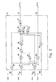
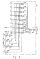
- a data processing system to which the present invention is applicable comprises processors 1 and 2, a control apparatus 3 embodying the present invention, and memory units 4 and 5.
- the processors 1 and 2 produce memory access request signals which can have simultaneous access to the units 4 and 5 through lines 200 and 202 and the apparatus 3 to cause data to be read from or written in the units 4 and 5 at the same time.
- the apparatus 3 receives status signals from the individual units 4 and 5 through lines 205 and 206 and feeds either one of them as a status notifying signal back to the processors 1 and 2 through a line 201.
- Each processor 1 or 2 may have the construction illustrated in Figure 1 of US-A-3 656 123 and each memory unit 4 or 5 the construction shown in. Figures 1A and 2 of US-A-3 796 996. It should be borne in mind that the embodiment of the present invention discussed hereinafter is operated in response to system clock pulses which will be described later.
- the control apparatus 3 of the invention is made up of holding circuits 10 and 19, a priority identifying circuit 11, a memory access unit 12, a status selection command unit 13, a selector 14, status holding circuits 15 and 16, error holding circuits 17 and 18 and a control circuit 23.
- the circuit 10 receives and holds access request, address, and data fed from the processor 1 through the line 200.
- the circuit 19 receives and holds access request, address, and data fed from the other processor 2 through the line 202.
- the circuit 11 determines the priority order of the access requests from the processors 1 and 2.
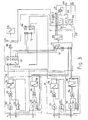
- the memory access unit 12 comprises a request holding circuit 20 and AND gates 21 and 22.
- each AND gate 21 or 22 receives the output of the circuit 20 at its one input terminal and a negative output signal of the circuit 17 or 18 at its other input terminal. In response to the input signals, the AND gate 21 supplies the unit 4 with an access request signal through the line 203 while the AND gate 22 supplies the unit 5 with an access request signal through the line 204.
- both the AND gates 21 and 22 are open to pass the output of the circuit 20 to the units 4 and 5 at the same time.
- an error is generated, for example, in the unit 4 so that the status signal fed to the circuit 17 through the line 205 indicates an error, the negative output of the circuit 17 becomes "0" whereby the AND gate 21 is closed.
- the holding circuits 15 and 16 are adapted to hold status signals given thereto from the units 4 and 5 through the lines 205 and 206, respectively.
- a circuit (not shown) installed in the units 4 and 5 for generating such status signals may comprise the register 23 and bus 44 shown in Figure 1 of the US-A-3 814 922.
- the circuit 17 or 18 continuously supplies the command unit 13 with a status error signal through a line 209 or 210 until a reset command signal is sent thereto from the outside.
- the unit 13 feeds a selection command signal to the selector 14, in response to a signal delivered from the control circuit 23 through a line 207 for designating a master memory unit, a write command signal supplied from the circuit 23 through a line 208, and a status error signal supplied from the circuit 17 or 18 through the line 209 or 210.
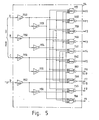
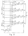
- the status selection command unit 13 is composed of a flip-flop (F/F) 106 and gates 100 to 105 and 107 to 111 and 117.
- the status error signal from the circuit 17 or 18 is given to the corresponding gate 100 or 117 via the line 209 or 210.
- a master designating signal is supplied from the outside to the gate 101 by way of the line 207 and the write command signal to the gate 110 via the line 208.
- the output of the AND gate 100 is fed to the NAND gate 102, AND gate 104, and NAND gate 107.
- the NAND gate 117 supplies a positive output to the other input of the AND gate 104 and a negative output to the NAND gates 103 and 109.
- the NAND gate 103 receives at its other input the positive output signal of the NAND gate 101.
- the negative output of the gate 101 is sent to the other input of the NAND gate 102.
- the outputs of the NAND gates 102 and 103 are supplied to the NAND gate 105 so that the F/F 106 is driven in response to the output of the NAND gate 105.
- the F/F 106 is of the D-type which produces the logical state of an input signal in response to the next clock pulse.
- the output of the F/F 106 is fed to the NAND gates 108 and 109.
- the other input of the NAND gate 108 is connected with the negative output terminal of the gate 110.
- the positive output terminal of the gate 110 is connected to the NAND gates 109 and 107.
- the NAND gate 107 is coupled to the negative output terminal of the F/F 106.
- the outputs of the NAND gates 107, 108 and 109 are fed to the NAND gate 111.
- the output of the gate 111 is fed through a line 211 as a status selection signal.
- the output of the AND gate 104 is fed through a line 212 as a status inhibition signal.
- the holding circuit 10 shown in Figure 1 comprises an F/F 134 and its associated gates 131 to 133 for receiving an access request and inhibiting the next request from the processor 1, and a register 138 and its associated gates 135 to 137 for receiving data and address request from the processor 1 and supplying them to the priority identifying circuit 11.
- the holding circuit 19 comprises an F/F 174 and its associated gates 171 to 173 and a register 178 and its associated gates 175 to 177.
- the circuit 11 comprises a priority encoder 112, an inverter 113, a decoder 114, a multiplexer 115, and an F/F 116.
- the control circuit 23 is composed of an F/F 231, a shift register 232, and F/F 233, and an AND gate 234.
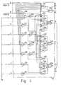
- the encoder 112 is composed of inverters 1120 to 1131, NAND gates 1132 and 1145, AND gates 1133 to 1144, and NOR gates 1146 to 1148.
- the encoder 112 determines the priority order and codes it in response to access request signals from the circuits 10 and 19, thereafter supplying a selection command to the multiplexer 115.
- the input terminal A is connected with the circuit 10 and the input terminal B is connected with the circuit 19, while the input terminals C to I are grounded.
- the decoder 114 comprises inverters 1149 to 1156 and NAND gates 1157 to 1166 and functions to decode the coded output of the encoder 112.
- the decoded data is partly fed back to the circuits 10 and 19 which then have their F/F's 134 and 174 reset.
- the multiplexer 115 includes inverters 1167 to 1173 and 1183, AND gates 1174 to 1181 and a NAND gate 1182. In response to a selection command from the encoder 112, the multiplexer 115 selects one of the data given from the circuits 10 and 19.
- a set of three lines 205 are connected to the status holding circuit 15 and a set of three lines 206 are connected to the other status holding circuit 16.
- Three lines connect the output terminals of the circuit 15 to corresponding input terminals 1A, 2A and 3A of the selector 14.
- three lines connect the output terminals of the circuit 16 to corresponding input terminals 1B, 2B and 3B of the selector 14.
- the selector 14 produces a status notifying signal on lines 201 which are connected with output terminals To to T 3 , and the status notifying signal is then supplied to the processors 1 and 2.
- the selector 14 is composed of inverters 140 to 142, 155 to 158, AND gates 143 to 150 and NOR gates 151 to 154.
- the selector 14 selects either the signal from the circuit 15 or the signal from the circuit 16 in response to a selection command signal. This signal is given from a terminal SO (see Fig. 8) to the selector 14 through the line 211.
- a selection inhibition signal is supplied from the unit 13 to the processors 1 and 2 through the line 212, regardless of the state of the selection command signal. Receiving the selection inhibition signal, the processors 1 and 2 recognize that both the memory units 4 and 5 have failed.
- a memory access request is supplied to and stored in the circuit 10 via the line 200 (see (200) in Figure 9A).
- the output of the circuit 10 is supplied to the priority identifying circuit 11 and then stored in the request holding circuit 20 (see (10) and (20) in Figure 9A).
- the access request from the circuit 20 is given to the memory units 4 and 5 via the gates 21 and 22, respectively.
- status signals are stored in the circuits 15 and 16 through the lines 205 and 206, respectively (see (205) and (206) in Figure 9A).
- status error signals supplied to the error holding circuits 17 and 18 are fed to the unit 13 through the lines 209 and 210, respectively (see (209) and (210) in Fig. 9A).
- the memory unit 4 shown in Figure 1 is designated to work as a master memory unit (see (207) in Figure 9A).
- the master designating signal is supplied to the F/F 233 shown in Figure 3 from the outside, such as an input/output processor (not shown), via a line 213. Thereafter, the master designating signal is supplied to the unit 13. If the status signals supplied from the units 4 and 5 through the lines 205 and 206 indicate no error, the status error signal fed from the circuit 17 to the unit 13 through the line 209 is "0" and, therefore, the output of the NAND gate 107 is "1".
- the output of the NAND gate 102 is "1" and the NAND gate 103 receives at its one input a positive signal corresponding to the master designating signal, i.e., "0" from the gate 101, so that the NAND gate 103 produces “1".
- the NAND gate 105 therefore, receives "1” at its two inputs to generate “0". This causes the F/F 106 to also generate “0” (see (106) in Figure 9A).
- both the NAND gates 108 and 109 generate “1", that is, all the three inputs to the NAND gate 111 are “1”; the output signal or status selection signal of the NAND gate 111 is "0" (see the first row of the Truth Table and (211) in Figure 9A).
- the selector 14 thus selects the output of the circuit 15 (see (201) in Figure 9A). Though not shown in Figure 1, in a read mode operation, data read from the unit 4 or 5 is also selected by the status selection signal.
- a read mode operation proceeds as follows in the event the master memory unit 4 has failed.
- the procedure up to the supply of a memory access request from the processor 1 to the memory units 4 and 5 through the line 200, the circuit 10, 11, and 20, and gates 21 and 22 is the same as in the case with no failure.
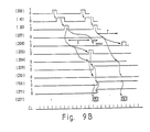
- the status signal fed from the unit 4 through the line 205 is "1" (see (205) in Figure 9B).
- This signal is stored in the status holding circuit 15.
- an error status signal is stored in the error holding circuit 17 and fed therefrom to the unit 13 through the line 209 (see (209) in Figure 98).
- the outputs of the F/F 231 and the register 116 are sent to the AND gate 234, whose output is supplied to the shift register 232.
- the register 232 is triggered to produce a signal after the memory access time T has elapsed.
- the content of the register 232 is fed as a write command signal to the line 208. While the negative output of the gate 110 is "1" due to the "0" or the write command signal, the output of the NAND gate 108 becomes “1” due to the "0" output of the F/F 106. This makes the status selection signal fed from the NAND gate 111 to the line 211 "0" (see (211) in Figure 9B).
- the output of the F/F 106 is set to "1", in response to the next clock pulse, because all the inputs to the NAND gate 102 are “1". Therefore, the status selection signal on the line 211 becomes "1" (see the third row of the Truth Table).
- the selector 14 supplies the processor 1 with the output signal of the circuit 15, that is, the status signal from the memory unit 4 which has failed at the time of reading operation, by way of the line 201.
- the status signal from the normal memory unit 5 is fed to the processors 1 and 2 through the line 201 (see (201) in Figure 9B).
- FIG. 9C The operation shown in Figure 9C is common to that described with reference to Figure 9B up to the step where a memory access request delivered from the processor 1 through the line 200 is given to the memory units 4 and 5 through the circuits 10, 11, and 20, and gates 21 and 22 and, thereafter, status signals are supplied from the units 4 and 5 to the corresponding holding circuits 15 and 16 through the lines 205 and 206 with an error signal fed to the unit 13 through the error holding circuit 17 and line 209 (see (200), (10), (20), (205), (206), and (209) in Figure 9C).
- the selector 14 thus supplies the processor 1 through the line 201 with a status notifying signal which has selected the output of the circuit 16, i.e., the status signal of the error-free memory unit 5 (see (201) in Figure 9C). Stated another way, no error is reported to the processor 1 which will then continue the processing operation. However, the gate 21 is closed by the negative output of the circuit 17. As a result, any further access to the memory unit 4 by the processor 1 is prevented and, instead, data from the processor 1 are continuously written in the other memory unit 5. It will be seen that the unit 5 has stored all the necessary data during the processing period. Accordingly, the whole system operates without any problem.
- a status selection signal is supplied through the line 211 at a timing one clock pulse behind the supply of an error signal via the line 209.
- the circuit 18 When the other memory unit 5 has a failure while the status error signal 209 is "1", the circuit 18 becomes set producing a "1" status error signal 201. Then, the output of the gate 104, i.e., the status inhibition signal fed through the line 212, becomes "1" whereby the error status notifying signal is forcibly returned by the selector 14 to the processor 1. Failure in both the memory units 4 and 5 results in a system-down, though the probability of such occurrence is only negligible. Meanwhile, in the event of an error in either the memory unit 4 or the unit 5, it should preferably be removed by a quick and proper measure. The same procedure as described hereinabove will occur, when the master designating signal is "1".
- the present invention can readily control a plurality of memory units with a simple construction and thereby realize a system excellent in performance and reliability. This is achieved by causing a plurality of memory units into simultaneous writing or reading operations and selecting one of them for use. When an error has occurred during a write mode operation, a memory unit without the error is immediately selected alternatively. In the event of an error during a read mode operation, the selection is made, in response to the next clock pulse, to permit a retry from a processor.
Landscapes
- Engineering & Computer Science (AREA)
- Theoretical Computer Science (AREA)
- Physics & Mathematics (AREA)
- General Engineering & Computer Science (AREA)
- General Physics & Mathematics (AREA)
- Quality & Reliability (AREA)
- Hardware Redundancy (AREA)
- Techniques For Improving Reliability Of Storages (AREA)
Applications Claiming Priority (2)
| Application Number | Priority Date | Filing Date | Title |
|---|---|---|---|
| JP56071471A JPS57189396A (en) | 1981-05-14 | 1981-05-14 | Controller for plural storage parts in data processing system |
| JP71471/81 | 1981-05-14 |
Publications (3)
| Publication Number | Publication Date |
|---|---|
| EP0066147A2 EP0066147A2 (en) | 1982-12-08 |
| EP0066147A3 EP0066147A3 (en) | 1985-05-15 |
| EP0066147B1 true EP0066147B1 (en) | 1988-12-14 |
Family
ID=13461551
Family Applications (1)
| Application Number | Title | Priority Date | Filing Date |
|---|---|---|---|
| EP82104206A Expired EP0066147B1 (en) | 1981-05-14 | 1982-05-13 | Control method and apparatus for a plurality of memory units |
Country Status (4)
| Country | Link |
|---|---|
| US (1) | US4488223A (esLanguage) |
| EP (1) | EP0066147B1 (esLanguage) |
| JP (1) | JPS57189396A (esLanguage) |
| DE (1) | DE3279289D1 (esLanguage) |
Families Citing this family (7)
| Publication number | Priority date | Publication date | Assignee | Title |
|---|---|---|---|---|
| DE1019594B (de) * | 1954-09-04 | 1957-11-14 | Tipp & Co | Fuer den Antrieb eines Fahrspielzeuges dienender Elektromotor |
| JPS59112498A (ja) * | 1982-12-20 | 1984-06-28 | Mitsubishi Electric Corp | 二重化共有メモリ装置 |
| DE3782893T2 (de) * | 1986-09-10 | 1993-04-08 | Nippon Electric Co | Informationsverarbeitungssystem, faehig zur verminderung ungueltiger speicheroperationen durch erkennung von hauptspeicherfehlern. |
| US5434979A (en) * | 1987-02-27 | 1995-07-18 | Unisys Corporation | Disk drive controller |
| JPH0616617B2 (ja) * | 1987-12-07 | 1994-03-02 | 富士通株式会社 | 初期条件設定方法 |
| GB2251502B (en) * | 1990-11-07 | 1995-06-14 | Nonstop Networks Limited | Data-loss prevention products |
| US7882388B2 (en) * | 2008-08-21 | 2011-02-01 | Sierra Wireless America, Inc. | Dual independent non volatile memory systems |
Family Cites Families (11)
| Publication number | Priority date | Publication date | Assignee | Title |
|---|---|---|---|---|
| US932005A (en) * | 1903-07-31 | 1909-08-24 | United Shoe Machinery Ab | Machine for making lacing-hooks. |
| US3387276A (en) * | 1965-08-13 | 1968-06-04 | Sperry Rand Corp | Off-line memory test |
| US3668644A (en) * | 1970-02-09 | 1972-06-06 | Burroughs Corp | Failsafe memory system |
| US3905023A (en) * | 1973-08-15 | 1975-09-09 | Burroughs Corp | Large scale multi-level information processing system employing improved failsaft techniques |
| US3950729A (en) * | 1973-08-31 | 1976-04-13 | Nasa | Shared memory for a fault-tolerant computer |
| US3934227A (en) * | 1973-12-05 | 1976-01-20 | Digital Computer Controls, Inc. | Memory correction system |
| UST932005I4 (en) | 1973-12-28 | 1975-03-04 | Detection op possibly erroneous segments following failures in primary storage | |
| US4010450A (en) * | 1975-03-26 | 1977-03-01 | Honeywell Information Systems, Inc. | Fail soft memory |
| US4044337A (en) * | 1975-12-23 | 1977-08-23 | International Business Machines Corporation | Instruction retry mechanism for a data processing system |
| JPS52124826A (en) * | 1976-04-12 | 1977-10-20 | Fujitsu Ltd | Memory unit |
| CA1102007A (en) * | 1979-05-15 | 1981-05-26 | Prem L. Sood | Duplicated memory system having status indication |
-
1981
- 1981-05-14 JP JP56071471A patent/JPS57189396A/ja active Granted
-
1982
- 1982-05-11 US US06/377,000 patent/US4488223A/en not_active Expired - Lifetime
- 1982-05-13 EP EP82104206A patent/EP0066147B1/en not_active Expired
- 1982-05-13 DE DE8282104206T patent/DE3279289D1/de not_active Expired
Also Published As
| Publication number | Publication date |
|---|---|
| EP0066147A2 (en) | 1982-12-08 |
| JPS6226493B2 (esLanguage) | 1987-06-09 |
| US4488223A (en) | 1984-12-11 |
| EP0066147A3 (en) | 1985-05-15 |
| DE3279289D1 (en) | 1989-01-19 |
| JPS57189396A (en) | 1982-11-20 |
Similar Documents
| Publication | Publication Date | Title |
|---|---|---|
| US4253147A (en) | Memory unit with pipelined cycle of operations | |
| US5173905A (en) | Parity and error correction coding on integrated circuit addresses | |
| EP0032957B1 (en) | Information processing system for error processing, and error processing method | |
| US6134672A (en) | System and method for iterative copying of read/write memory | |
| US3668644A (en) | Failsafe memory system | |
| EP0363863B1 (en) | Method and apparatus for fault recovery in a digital computing system | |
| EP0185924A2 (en) | Buffer system with detection of read or write circuits' failures | |
| US4295219A (en) | Memory write error detection circuit | |
| EP0186006A2 (en) | Multiprocessor system | |
| EP0041999A1 (en) | Self-correcting memory system and method | |
| EP0266836A2 (en) | Data processing system including a watch-dog circuit | |
| GB2034942A (en) | Errorcorrecting memory | |
| EP0037705A1 (en) | Error correcting memory system | |
| EP0266837A2 (en) | Data processing system including a watch-dog circuit | |
| US4942575A (en) | Error connection device for parity protected memory systems | |
| JPS63221445A (ja) | メモリシステム及び関連の誤まり検出及び訂正装置 | |
| EP0066147B1 (en) | Control method and apparatus for a plurality of memory units | |
| US4774712A (en) | Redundant storage device having address determined by parity of lower address bits | |
| US4165533A (en) | Identification of a faulty address decoder in a function unit of a computer having a plurality of function units with redundant address decoders | |
| US4254464A (en) | Common data buffer system | |
| US4942578A (en) | Buffer control method and apparatus | |
| JPH0117181B2 (esLanguage) | ||
| EP0653706A2 (en) | Error handling and correction in computer system | |
| AU669410B2 (en) | Error recovery mechanism for software visible registers in computer systems | |
| JPS6252340B2 (esLanguage) |
Legal Events
| Date | Code | Title | Description |
|---|---|---|---|
| PUAI | Public reference made under article 153(3) epc to a published international application that has entered the european phase |
Free format text: ORIGINAL CODE: 0009012 |
|
| AK | Designated contracting states |
Designated state(s): DE FR GB NL |
|
| RAP1 | Party data changed (applicant data changed or rights of an application transferred) |
Owner name: NEC CORPORATION |
|
| PUAL | Search report despatched |
Free format text: ORIGINAL CODE: 0009013 |
|
| AK | Designated contracting states |
Designated state(s): DE FR GB NL |
|
| 17P | Request for examination filed |
Effective date: 19850703 |
|
| 17Q | First examination report despatched |
Effective date: 19860717 |
|
| RIN1 | Information on inventor provided before grant (corrected) |
Inventor name: CHIWAKI, YOSHINORI |
|
| GRAA | (expected) grant |
Free format text: ORIGINAL CODE: 0009210 |
|
| AK | Designated contracting states |
Kind code of ref document: B1 Designated state(s): DE FR GB NL |
|
| REF | Corresponds to: |
Ref document number: 3279289 Country of ref document: DE Date of ref document: 19890119 |
|
| ET | Fr: translation filed | ||
| PLBE | No opposition filed within time limit |
Free format text: ORIGINAL CODE: 0009261 |
|
| STAA | Information on the status of an ep patent application or granted ep patent |
Free format text: STATUS: NO OPPOSITION FILED WITHIN TIME LIMIT |
|
| 26N | No opposition filed | ||
| PGFP | Annual fee paid to national office [announced via postgrant information from national office to epo] |
Ref country code: DE Payment date: 20010508 Year of fee payment: 20 |
|
| PGFP | Annual fee paid to national office [announced via postgrant information from national office to epo] |
Ref country code: GB Payment date: 20010509 Year of fee payment: 20 |
|
| PGFP | Annual fee paid to national office [announced via postgrant information from national office to epo] |
Ref country code: FR Payment date: 20010518 Year of fee payment: 20 |
|
| PGFP | Annual fee paid to national office [announced via postgrant information from national office to epo] |
Ref country code: NL Payment date: 20010531 Year of fee payment: 20 |
|
| REG | Reference to a national code |
Ref country code: GB Ref legal event code: IF02 |
|
| PG25 | Lapsed in a contracting state [announced via postgrant information from national office to epo] |
Ref country code: GB Free format text: LAPSE BECAUSE OF EXPIRATION OF PROTECTION Effective date: 20020512 |
|
| PG25 | Lapsed in a contracting state [announced via postgrant information from national office to epo] |
Ref country code: NL Free format text: LAPSE BECAUSE OF EXPIRATION OF PROTECTION Effective date: 20020513 |
|
| REG | Reference to a national code |
Ref country code: GB Ref legal event code: PE20 Effective date: 20020512 |
|
| NLV7 | Nl: ceased due to reaching the maximum lifetime of a patent |
Effective date: 20020513 |