EP0065517B1 - Surface roughness gauge - Google Patents
Surface roughness gauge Download PDFInfo
- Publication number
- EP0065517B1 EP0065517B1 EP19810901198 EP81901198A EP0065517B1 EP 0065517 B1 EP0065517 B1 EP 0065517B1 EP 19810901198 EP19810901198 EP 19810901198 EP 81901198 A EP81901198 A EP 81901198A EP 0065517 B1 EP0065517 B1 EP 0065517B1
- Authority
- EP
- European Patent Office
- Prior art keywords
- gauge
- sensor head
- common plane
- roughness
- line
- Prior art date
- Legal status (The legal status is an assumption and is not a legal conclusion. Google has not performed a legal analysis and makes no representation as to the accuracy of the status listed.)
- Expired
Links
- 230000003746 surface roughness Effects 0.000 title claims abstract description 19
- 238000012545 processing Methods 0.000 claims description 5
- 238000005259 measurement Methods 0.000 claims description 3
- 230000000007 visual effect Effects 0.000 claims 1
- 238000002310 reflectometry Methods 0.000 abstract description 9
- 238000000034 method Methods 0.000 abstract description 5
- 230000008569 process Effects 0.000 abstract description 4
- 235000019592 roughness Nutrition 0.000 description 24
- 230000007423 decrease Effects 0.000 description 4
- 238000010276 construction Methods 0.000 description 3
- 238000012937 correction Methods 0.000 description 3
- 230000008859 change Effects 0.000 description 2
- 230000008878 coupling Effects 0.000 description 2
- 238000010168 coupling process Methods 0.000 description 2
- 238000005859 coupling reaction Methods 0.000 description 2
- 238000003754 machining Methods 0.000 description 2
- 241000220010 Rhode Species 0.000 description 1
- 230000008901 benefit Effects 0.000 description 1
- 230000007812 deficiency Effects 0.000 description 1
- 230000005670 electromagnetic radiation Effects 0.000 description 1
- 238000007373 indentation Methods 0.000 description 1
- 238000012552 review Methods 0.000 description 1
- 238000000926 separation method Methods 0.000 description 1
- 238000004441 surface measurement Methods 0.000 description 1
- 238000012360 testing method Methods 0.000 description 1
- 210000003813 thumb Anatomy 0.000 description 1
Images

Classifications
-
- G—PHYSICS
- G01—MEASURING; TESTING
- G01B—MEASURING LENGTH, THICKNESS OR SIMILAR LINEAR DIMENSIONS; MEASURING ANGLES; MEASURING AREAS; MEASURING IRREGULARITIES OF SURFACES OR CONTOURS
- G01B11/00—Measuring arrangements characterised by the use of optical techniques
- G01B11/30—Measuring arrangements characterised by the use of optical techniques for measuring roughness or irregularity of surfaces
- G01B11/303—Measuring arrangements characterised by the use of optical techniques for measuring roughness or irregularity of surfaces using photoelectric detection means
Definitions
- This invention relates generally to a gauge, for measuring the surface roughness of an article, and more particularly to a non-contacting surface roughness gauge based on detecting and processing specular and diffused light.
- Non-contacting surface measurement gauges e.g. as known from US-A-4092068 are available which compare the relative quality of a test surface with respect to a known surface of the same type. Such gauges are offered commercially by Measurement Arts, Inc. of Buffalo, Rhode Island under the name Explorer I Surface Quality Measurement System. While that system has been accepted in the industry, it does not directly measure roughness in micrometers, it is undesirably sensitive to surface reflectivity, and it is limited to measuring surface quality at a right angle to the lay or to the direction of surface irregularities such as machining grooves. Another deficiency is that the measuring head thereof is too large so that it can't measure in tight spots. Specifically, that system cannot measure the cylindrical surface finish of a crankshaft bearing at the desired location relatively close to a crankshaft shoulder, for example.
- a relatively inexpensive, compact and simple gauge that can provide a direct reading of the surface roughness of an article in micrometers or microinches independent of the direction of lay of the grinding or machining marks with but minor recalibration and independent of the reflectivity of the surface.
- Another desired feature is to provide a gauge which can easily be recalibrated for measuring articles of different surface contour.
- the present invention as claimed is directed to overcoming one or more of the problems as set forth above.
- the invention contemplates three photo diodes arranged on a body to open outwardly upon a semi-spherical cavity and aimed toward a common point for receiving the reflected light from the surface of the article to be measured so as to provide a resultant reading in micrometers after processing the signals therefrom in an associated control apparatus.
- the readings thus obtained can be made with any angular orientation of the gauge with respect to the lay of the surface irregularities, and substantially independent of the reflectivity of the surface.
- at least one photo diode is located to one side of the central plane passing through a light emitting diode and a specular photo diode, and the electrical control apparatus processes the signals from the diodes to give a roughness factor. This roughness factor is electrically controlled to cause a readout meter to provide the resultant reading in either micrometers or microinches, for example.
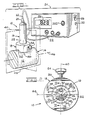
- a surface roughness gauge 10 for measuring the roughness of a cylindrical surface 12 of an article 14.
- the gauge includes a sensor body 16 releasably connected to a positioning device 18, a coupling 20 releasably connected to a control cable 22, and an electrically operated control apparatus or control box 24 adapted to receive and process the electrical information received from the sensor body by way of the control cable.
- the control box has a digital panel meter or readout meter 26 to permit convenient operator review of the output data in either micrometers or microinches.
- the bottom end of the sensor body 16 includes a cylindrical sensor head 28 having a diameter of about 2.54 cm (1").
- the sensor head 28 has mounted in relatively fixed positions thereon first means 30 for directing a light beam 32 upon the surface 12 of the article 14 and a second means 34 for receiving the specular light reflected from the surface and providing a first voltage signal proportion thereto.
- first means 30 includes a light emitting diode (LED) 36 and the second means 34 includes a first photo diode 38.
- Diodes 36 and 38 are arranged in a common midplane 40 disposed normal to the surface to be measured at a point of incidence 42, and with the axes of the diodes arranged such that the angle of incidence A is equal to the angle of reflection B.
- a second plane 44 is located through the point of incidence and disposed at a right angle to the common plane 40.
- the article 14 is a cylindrical pin having a central axis 46 and the second plane 44 contains the central axis.
- the diodes 36 and 38 are disposed in facing relation at equal distances from the second plane 44 as is indicated in the drawings. Since the specular photo diode 38 is at the same angle with respect to the surface being measured as the light emitting diode 36, the voltage output thereof represents the reflectivity of the surface being measured.
- the sensor head 28 has a central axis 47 and a planar end face 48 oriented normal to the central axis and located axially in line with the point of incidence 42. With such construction the sensor head can be manually adjusted vertically within a cylindrical opening 50 in the positioning device 18 in order to place the point of incidence 42 of the diodes 36, 38 in coinciding relationship with the surface level to be measured. Since the article in the example is cylindrical, the positioning device is basically an inverted V-block with an apex 52 thereof being capable of convenient orientation parallel to the axis 46 as is shown in Fig. 1. A manually releasable thumb screw 54 can be utilized to lock the sensor body 16 and positioning device 18 together upon reaching the desired elevational and rotational relationship. Alternatively, a pair of planar end surfaces 56 on the positioning device 18 can be used to orient the sensor body normal to a flat surface to be measured, not shown.
- the sensor head 28 further has third means 58 for receiving the diffused light reflected from the surface 12 in the common plane 40 of the diodes 36, 38 and providing a second voltage signal proportional thereto.
- third means includes a second photo diode 60 of the same type as specular diode 38, and being located on the forward side thereof for purposes of compactness.
- the diode 60 is axially oriented toward the point of incidence 42.
- the sensor head also has fourth means 61 mounted thereon for receiving the diffused light reflected from the surface 12 to the left side of the common plane 40 and fifth means 62 for receiving the diffused light reflected from the right side of the common plane and jointly providing a third voltage signal proportional thereto.
- the fourth means includes a third photo diode 63 and the fifth means includes a fourth photo diode 64 of the same type as the diodes 38 and 60 and also oriented toward the point of incidence 42.
- the first, second, third and fourth photo diodes 38, 60, 63 and 64 are nestably mounted compactly together in a substantially preselected quadralateral relationship on the sensor head 28 to receive the light from the opposite light emitting diode 36.
- the control apparatus 24 includes electrical circuit means 66 as is shown in Fig. 5.
- the electrical circuit means is electrically connected to the diodes 36, 38, 60, 63 and 64 and receives and processes the first, second and third signals from the first, second, and joint third and fourth photo diodes respectively.
- a preselected voltage source 68 for example 15 volts positive, is connected to the anode of the light emitting diode 36 via a line 70, and a line 72 connects the cathode thereof to a ground 74 through a fixed resistor 76.
- the same voltage source in line 70 is connected to the cathode of the first photo diode 38 and a first output signal line 80 extends from the anode thereof to a first operational amplifier 82 for purposes of gain control.
- the same voltage source is connected to the cathodes of the third and fourth photo diodes 63, 64 and a third output signal line 86 is connected to the anode thereof and to a third operational amplifier 88.
- Another voltage source 90 is connected to the anode of the second photo diode 60 by a line 92, and a second output signal line 94 extends from the cathode thereof to a second operational amplifier 96.
- the lines 70, 72, 80, 86, 92 and 94 extend through and form a major portion of the control cable 22 in Fig. 1, and are separable at the coupling 20. This separation is indicated in Fig. 5 by the broken vertical line 97, which line also separates the components on the sensor head 28 with those within the control apparatus 24.
- the operational amplifiers 82, 88 and 96 are of conventional construction and include variable resistors 98, 100 and 102 respectively for adjusting the gain of the individual signals received from the photo diodes 38, 60 and 63/64.
- the suitably amplified first signal from the amplifier 82 is connected to a summing and divider circuit 104 and also to a display select switch 106 via a line 108.
- the amplified second signal from the amplifier 96 is connected to the summing and divider circuit and the select switch via a line 110
- the amplified third signal from the amplifier 88 is connected to the summing and divider circuit and the select switch via a line 112.
- An intercept variable voltage control 114 having a resistor 115 is connected to the summing and divider circuit 104, as are the voltage sources 68 and 90, and an output line 116 from the circuit is connected to the select switch 106.
- the select switch is capable of electrically connecting one of four contact points identified as Nos. 1-4 in Fig. 5 with an output line 126.
- a conventional voltmeter 128 can be connected to the output line 126 at a contact point 130 to selectively take readings of the four contact points for initial calibration purposes.
- the surface roughness gauge 10 has the capability for convenient changeover in the readings at the digital panel meter 26 from micrometers to microinches.
- a compensation and switchover network 132 is used between the output line 126 and the panel meter.
- the digital panel meter is a conventional unit, such as Model No. DM-3100X offered by Datel Systems, Inc. of 11 Cabot Blvd., Mansfield, Maine. It has six connection points 134, 136, 138, 140, 142 and 144 to the compensation network.
- a substantially constant voltage of 6.8 volts is established at a line 146 of the compensation network 132, by connecting the voltage source 68 to the line 146 through a resistor 148 and by connecting a Zener diode 150 of preselected capacity to the ground 74.
- the line 146 is connected to a first input point 152 of a comparator operational amplifier 154 through a fixed resistor 156.
- the first input point 152 is further connected to the ground through first, second, third and fourth serially arranged resistors 158, 160, 162 and 164.
- Resistors 158 and 162 are variable resistors, and resistors 160 and 164 are fixed resistors.
- the upper resistors 158 and 160 are used for adjusting the input voltage to the first input point 152 when in the micrometer mode of operation, and these resistors are bypassed from the circuit by closing a first switch 166 in a bypass line 168 connected between point 152 and another point 170 between resistors 160 and 162.
- resistors 162 and 164 are adjustable to adjust the input voltage in the microinch mode
- resistors 158 and 160 are adjustable to adjust the input voltage in the micrometer mode.
- a line 172 connects the relatively stable voltage at line 146 to an output readout line 174 from the operational amplifier 154 through a pair of serially arranged fixed resistors 176 and 178 of relatively high resistance, for example one megohm each.
- the connection point 142 is connected to a point 180 between the resistors 176, 178 and the connection point 144 is connected to the line 172 before the resistors 176, 178.
- a second input point 182 to the comparator operational amplifier 154 is connected to the output line 126 from the select switch 106 through first, second, third and fourth serially arranged resistors 184, 186, 188 and 190.
- Resistors 184 and 188 are of fixed capacity, and resistors 186 and 190 are of variable capacity.
- the right resistors 188 and 190 are used for adjusting the input voltage to the second input point 182 when in the micrometer mode of operation, and these resistors are bypassed from the circuit by closing a second switch 192 in a bypass line 194 connected between second input point 182 and another 196 located between resistors 186 and 188. Therefore, when the second switch 192 is closed resistors 184 and 186 are adjustable to control the reference gain in the microinch mode, and when the second switch is open resistors 188 and 190 are adjustable to control the reference gain in the micrometer mode.
- a decimal point correction is required of the digital panel meter 26.
- This is achieved by using a third switch 198 to directly connect connection points 134 and 138 or 136 and 138.
- the switches 166,192 and 198 are preferably connected together for joint operation as diagrammatically indicated by the broken line 200 in Fig. 5 and, as shown in Fig. 1, a single control lever 202 on the face of the control box 24 is effective to jointly move them.
- the switches 166 and 192 are open as indicated in Fig. 5, and the switch 198 connects connection points 134 and 138 directly together.
- the switches 166 and 192 are closed, and the switch 198 connects connection points 136 and 138.
- the voltmeter 128 initially can be used to take a series of voltage output readings at the contact points 1, 2 and 3 of the display select switch 106. These output readings correspond to the amplified values of the first, second and third signals received from the photo diodes 38, 60 and 63/64. To take these readings the sensor head 28 can be positioned on a series of cylindrical surfaces individually having different standard or known roughness values and with the common plane 40 of the sensor head.28 positioned normal to or at a right angle to the lay. If the output readings are plotted in arbitrary voltage units on a vertical or ordinate scale and the known roughness values in micrometers plotted on a horizontal or abscissa scale, the result will be generally like the graph illustrated in Fig. 7.
- the third and fourth diffused side photo diodes 63, 64 provide an output voltage at the contact point 3 that is substantially constant as is indicated by the generally horizontal line 204, while the output of the specular photo diode 38 at the contact point 1 decreases with increasing surface roughness as is indicated by the line 206 and the output of the diffused forward photo diode 60 at the contact point 2 increases as is indicated by the line 208.
- FIG. 8 Upon rotating the sensor head 28 to an orientation parallel to the lay or, so that the common midplane 40 is parallel to the direction of run of the indentations in the surface, and taking another series of voltage readings of cylinders with different known roughness values, another graph can be made such as that illustrated in Fig. 8.
- the diffused forward photo diode 60 provides an output voltage at the contact point 2 that is substantially constant or generally horizontal as is indicated by the line 210.
- the output of the diffused side photo diodes 63, 64 at the contact point 3 increases with increasing surface roughness, as indicated by line 212, and the output of the specular photo diode 38 at the contact point 1, decreases as indicated by line 214.
- the summing and dividing circuit 104 such as is available as Part No. AD535 from Analog Devices of Norwood, Massachusetts performs the relationship of the above equation, and provides a roughness factor at the contact point 4 of the display select switch 106. Since the output of each diode will decrease with a decrease in surface reflectivity, the roughness factor is advantageously independent of surface reflectivity. With these data the average roughness values at the panel meter 26 can be directly related to the roughness factors by the following second equation:
- the sensor head 28 In order to initially calibrate the electrical circuit means 66, the sensor head 28 is positioned on a standard or known reference at the low end of the desired roughness range, for example at 0.05 micrometer (2 microinch) surface roughness, and then at the high end, for example, at 0.43 micrometer (17 microinch) surface roughness. If the respective first and second gauge readings are as shown at points 220 and 222 on the graph of Fig. 9, a straight broken line 224 drawn therebetween will indicate that the gauge readings are slightly offset from the desired line 215. In order to change the position of the line 224 the resistor 115 of the intercept variable voltage control 114 illustrated in Fig. 5 can be manually adjusted relative to its voltage input to move line 224 up and down, or vertically when viewing the graph at the same approximate slope.
- the intercept variable voltage control 114 functions to provide the desired value "I" in the second equation set forth above.
- the gain of first operational amplifier 82 can thereafter be changed by manually adjusting the variable resistor 98 to rotate the line 224 or to increase the slope thereof so that it substantially coincides with the desired line 215.
- a calibration technique is available for conveniently modifying the gauge 10 so that it can measure cylindrical pins with the gauge oriented with the lay or normal to the lay of the surface irregularities, and with the gauge readings being precisely matched to known or controlled roughness values.
- similar relationships exist with respect to measuring flat surfaces or other arcuate surfaces.
- a miniaturized second embodiment of the gauge 10 was constructed as is illustrated in Fig. 6. Reference numerals having a prime indicator thereon have been used in Fig. 6 to identify parts similar in function to those described with respect to the first embodiment.
- a distance "S" of less than about 4 mm (0.16") can be obtained by deleting one of the side diffused photo diodes 63, 64 of the first embodiment by miniaturizing the remaining photo diodes 38', 60', 63' and light emitting diode 36', and by placing them relatively compactly together.
- the forward diffused diode 60' is axially oriented along the central axis 47, and remaining diodes placed immediately therearound in a semi-spherical, outwardly opening cavity 228 measuring less than about 5 mm (0.2") in diameter (D) as can be recognized by reference to Fig. 6.
- the diodes 36', 38', 60' and 63' are miniaturized and are available from Spectronics of 830 E. Arapaho Rd., Richard- son, Texas.
- the surface roughness gauge 10 advantageously incorporates at least one photo diode 63 or 64 for measuring diffused light reflected from the surface of ths article to the side of the common plane 40 in order to be useful for measuring roughness with the gauge oriented parallel to the lay. It further incorporates a diffused forward diode 60 useful for measuring scattered light when the gauge is oriented perpendicular to the lay.
- the versatile relationship of the voltage signals received from the diffused forward diode, the diffused side diode, and the specular diode has been so programmed in the control apparatus 24 as to be of a substantially increasing straight line signal reading with increasing surface roughness of the article being measured. Such readings are independent of the reflectivity level of the surface being measured.
- the compensation and switch over network 132 serves to conveniently convert the roughness factors directly to actual micrometer or microinch readings.
- the observed readings are substantially instantantaneously displayed on the readout meter 26.
Landscapes
- Physics & Mathematics (AREA)
- General Physics & Mathematics (AREA)
- Length Measuring Devices By Optical Means (AREA)
- Investigating Or Analysing Materials By Optical Means (AREA)
Abstract
Description
- This invention relates generally to a gauge, for measuring the surface roughness of an article, and more particularly to a non-contacting surface roughness gauge based on detecting and processing specular and diffused light.
- Non-contacting surface measurement gauges e.g. as known from US-A-4092068 are available which compare the relative quality of a test surface with respect to a known surface of the same type. Such gauges are offered commercially by Measurement Arts, Inc. of Providence, Rhode Island under the name Explorer I Surface Quality Measurement System. While that system has been accepted in the industry, it does not directly measure roughness in micrometers, it is undesirably sensitive to surface reflectivity, and it is limited to measuring surface quality at a right angle to the lay or to the direction of surface irregularities such as machining grooves. Another deficiency is that the measuring head thereof is too large so that it can't measure in tight spots. Specifically, that system cannot measure the cylindrical surface finish of a crankshaft bearing at the desired location relatively close to a crankshaft shoulder, for example.
- Other surface quality gauges are known, such as those employing laser beams, which are excessively complex and fragile in construction. As far as is known, all known gauges must be recalibrated for each change in surface character, lay and/or reflectivity. Such recalibration has heretofore been too time-consuming and costly.
- Accordingly, what is desired is a relatively inexpensive, compact and simple gauge that can provide a direct reading of the surface roughness of an article in micrometers or microinches independent of the direction of lay of the grinding or machining marks with but minor recalibration and independent of the reflectivity of the surface. Another desired feature is to provide a gauge which can easily be recalibrated for measuring articles of different surface contour.
- The present invention as claimed is directed to overcoming one or more of the problems as set forth above.
- Preferably, the invention contemplates three photo diodes arranged on a body to open outwardly upon a semi-spherical cavity and aimed toward a common point for receiving the reflected light from the surface of the article to be measured so as to provide a resultant reading in micrometers after processing the signals therefrom in an associated control apparatus. Advantageously, the readings thus obtained can be made with any angular orientation of the gauge with respect to the lay of the surface irregularities, and substantially independent of the reflectivity of the surface. Specifically, at least one photo diode is located to one side of the central plane passing through a light emitting diode and a specular photo diode, and the electrical control apparatus processes the signals from the diodes to give a roughness factor. This roughness factor is electrically controlled to cause a readout meter to provide the resultant reading in either micrometers or microinches, for example.
-
- Fig. 1 is a perspective elevational view of a surface roughness gauge constructed in accordance with one embodiment of the present invention and disposed on a cylindrical article to be measured.
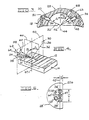
- Fig. 2 is a diagrammatic, enlarged, bottom plan view of the sensor head illustrated in Fig. 1.
- Fig. 3 is a fragmentary, diagrammatic, side elevational sectional view as taken along line III-III of Fig. 2.
- Fig. 4 is a fragmentary and diagrammatic view of a surface of an article of particular lay with certain components of the sensor head of Figs. 1-3 placed in proper geometric position thereon for explanation purposes.
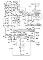
- Fig. 5 is an electrical circuit for receiving and processing the signals from the sensor head of Figs. 1-3, and directing them to the readout meter illustrated in Fig. 1.
- Fig. 6 is a diagrammatic, enlarged, bottom plan view of a second embodiment sensor head that can be compared with the first embodiment of Fig. 2.
- Fig. 7 is a graph of the voltage signals individually delivered by the light receiving photo diodes of the sensor head illustrated in Fig. 2 for various degrees of surface roughness, with the sensor head disposed on a cylindrical pin and oriented such that the common midplane thereof was normal to the lay.
- Fig. 8 is a graph similar to Fig. 7, only with the sensor head oriented such that the common midplane was parallel to the lay.
- Fig. 9 is a graph showing the average roughness gauge readings achieved by processing the individually signals illustrated in Figs. 7 and 8 in the control apparatus of the present invention in comparison with a range of known- roughness values.
- Referring initially to Fig. 1, one embodiment of a
surface roughness gauge 10 is disclosed for measuring the roughness of acylindrical surface 12 of anarticle 14. The gauge includes asensor body 16 releasably connected to apositioning device 18, acoupling 20 releasably connected to acontrol cable 22, and an electrically operated control apparatus orcontrol box 24 adapted to receive and process the electrical information received from the sensor body by way of the control cable. Advantageously, the control box has a digital panel meter orreadout meter 26 to permit convenient operator review of the output data in either micrometers or microinches. - As is shown in Fig. 2, the bottom end of the
sensor body 16 includes acylindrical sensor head 28 having a diameter of about 2.54 cm (1"). As is shown also in Figs. 3 and 4, thesensor head 28 has mounted in relatively fixed positions thereon first means 30 for directing alight beam 32 upon thesurface 12 of thearticle 14 and asecond means 34 for receiving the specular light reflected from the surface and providing a first voltage signal proportion thereto. By the term "light beam" as used herein it is meant to include a beam of electromagnetic radiation having a wave length at or near the infrared and visible ranges. Thefirst means 30 includes a light emitting diode (LED) 36 and thesecond means 34 includes afirst photo diode 38.Diodes common midplane 40 disposed normal to the surface to be measured at a point ofincidence 42, and with the axes of the diodes arranged such that the angle of incidence A is equal to the angle of reflection B. Asecond plane 44 is located through the point of incidence and disposed at a right angle to thecommon plane 40. In the example of Fig. 1, thearticle 14 is a cylindrical pin having acentral axis 46 and thesecond plane 44 contains the central axis. Thus, thediodes second plane 44 as is indicated in the drawings. Since thespecular photo diode 38 is at the same angle with respect to the surface being measured as thelight emitting diode 36, the voltage output thereof represents the reflectivity of the surface being measured. - The
sensor head 28 has acentral axis 47 and a planar end face 48 oriented normal to the central axis and located axially in line with the point ofincidence 42. With such construction the sensor head can be manually adjusted vertically within acylindrical opening 50 in thepositioning device 18 in order to place the point ofincidence 42 of thediodes apex 52 thereof being capable of convenient orientation parallel to theaxis 46 as is shown in Fig. 1. A manuallyreleasable thumb screw 54 can be utilized to lock thesensor body 16 andpositioning device 18 together upon reaching the desired elevational and rotational relationship. Alternatively, a pair ofplanar end surfaces 56 on thepositioning device 18 can be used to orient the sensor body normal to a flat surface to be measured, not shown. - As shown in Figs. 2-4, the
sensor head 28 further hasthird means 58 for receiving the diffused light reflected from thesurface 12 in thecommon plane 40 of thediodes second photo diode 60 of the same type asspecular diode 38, and being located on the forward side thereof for purposes of compactness. Like thediode 38, thediode 60 is axially oriented toward the point ofincidence 42. Advantageously, the sensor head also hasfourth means 61 mounted thereon for receiving the diffused light reflected from thesurface 12 to the left side of thecommon plane 40 and fifth means 62 for receiving the diffused light reflected from the right side of the common plane and jointly providing a third voltage signal proportional thereto. The fourth means includes athird photo diode 63 and the fifth means includes afourth photo diode 64 of the same type as thediodes incidence 42. In this way, and as best shown in Fig. 2, the first, second, third andfourth photo diodes sensor head 28 to receive the light from the oppositelight emitting diode 36. - Turning now to the control portion of the
gauge 10, thecontrol apparatus 24 includes electrical circuit means 66 as is shown in Fig. 5. The electrical circuit means is electrically connected to thediodes voltage source 68, for example 15 volts positive, is connected to the anode of thelight emitting diode 36 via aline 70, and a line 72 connects the cathode thereof to aground 74 through afixed resistor 76. The same voltage source inline 70 is connected to the cathode of thefirst photo diode 38 and a first output signal line 80 extends from the anode thereof to a firstoperational amplifier 82 for purposes of gain control. The same voltage source is connected to the cathodes of the third andfourth photo diodes operational amplifier 88. Anothervoltage source 90, of opposite polarity but at the same value assource 68, is connected to the anode of thesecond photo diode 60 by a line 92, and a secondoutput signal line 94 extends from the cathode thereof to a secondoperational amplifier 96. It is to be noted that thelines control cable 22 in Fig. 1, and are separable at thecoupling 20. This separation is indicated in Fig. 5 by the broken vertical line 97, which line also separates the components on thesensor head 28 with those within thecontrol apparatus 24. - The
operational amplifiers variable resistors photo diodes amplifier 82 is connected to a summing anddivider circuit 104 and also to a display selectswitch 106 via aline 108. Similarly, the amplified second signal from theamplifier 96 is connected to the summing and divider circuit and the select switch via aline 110, and the amplified third signal from theamplifier 88 is connected to the summing and divider circuit and the select switch via aline 112. - An intercept variable voltage control 114 having a
resistor 115 is connected to the summing anddivider circuit 104, as are thevoltage sources select switch 106. Thus, the select switch is capable of electrically connecting one of four contact points identified as Nos. 1-4 in Fig. 5 with anoutput line 126. Aconventional voltmeter 128 can be connected to theoutput line 126 at acontact point 130 to selectively take readings of the four contact points for initial calibration purposes. - The
surface roughness gauge 10 has the capability for convenient changeover in the readings at thedigital panel meter 26 from micrometers to microinches. To accomplish this a compensation andswitchover network 132 is used between theoutput line 126 and the panel meter. In the illustrated embodiment the digital panel meter is a conventional unit, such as Model No. DM-3100X offered by Datel Systems, Inc. of 11 Cabot Blvd., Mansfield, Maine. It has sixconnection points - A substantially constant voltage of 6.8 volts is established at a
line 146 of thecompensation network 132, by connecting thevoltage source 68 to theline 146 through aresistor 148 and by connecting aZener diode 150 of preselected capacity to theground 74. Theline 146 is connected to afirst input point 152 of a comparatoroperational amplifier 154 through a fixedresistor 156. Thefirst input point 152 is further connected to the ground through first, second, third and fourth serially arrangedresistors Resistors resistors 160 and 164 are fixed resistors. Theupper resistors 158 and 160 are used for adjusting the input voltage to thefirst input point 152 when in the micrometer mode of operation, and these resistors are bypassed from the circuit by closing a first switch 166 in abypass line 168 connected betweenpoint 152 and anotherpoint 170 betweenresistors 160 and 162. Hence, when the switch 166 is closed,resistors resistors 158 and 160 are adjustable to adjust the input voltage in the micrometer mode. - A
line 172 connects the relatively stable voltage atline 146 to an output readout line 174 from theoperational amplifier 154 through a pair of serially arranged fixedresistors 176 and 178 of relatively high resistance, for example one megohm each. Theconnection point 142 is connected to apoint 180 between theresistors 176, 178 and theconnection point 144 is connected to theline 172 before theresistors 176, 178. - A
second input point 182 to the comparatoroperational amplifier 154 is connected to theoutput line 126 from theselect switch 106 through first, second, third and fourth serially arrangedresistors Resistors resistors right resistors second input point 182 when in the micrometer mode of operation, and these resistors are bypassed from the circuit by closing asecond switch 192 in abypass line 194 connected betweensecond input point 182 and another 196 located betweenresistors second switch 192 is closedresistors open resistors - Because of the well-known conversion factor of 39.37 between micrometers and microinches, a decimal point correction is required of the
digital panel meter 26. This is achieved by using athird switch 198 to directly connectconnection points single control lever 202 on the face of thecontrol box 24 is effective to jointly move them. When thecontrol lever 202 is up roughness is measured in micrometers, theswitches 166 and 192 are open as indicated in Fig. 5, and theswitch 198 connects connection points 134 and 138 directly together. On the other hand, when thecontrol lever 202 is down roughness is measured in microinches, theswitches 166 and 192 are closed, and theswitch 198 connects connection points 136 and 138. - The
voltmeter 128 initially can be used to take a series of voltage output readings at the contact points 1, 2 and 3 of the displayselect switch 106. These output readings correspond to the amplified values of the first, second and third signals received from thephoto diodes sensor head 28 can be positioned on a series of cylindrical surfaces individually having different standard or known roughness values and with thecommon plane 40 of the sensor head.28 positioned normal to or at a right angle to the lay. If the output readings are plotted in arbitrary voltage units on a vertical or ordinate scale and the known roughness values in micrometers plotted on a horizontal or abscissa scale, the result will be generally like the graph illustrated in Fig. 7. Note that the third and fourth diffusedside photo diodes contact point 3 that is substantially constant as is indicated by the generallyhorizontal line 204, while the output of thespecular photo diode 38 at the contact point 1 decreases with increasing surface roughness as is indicated by theline 206 and the output of the diffusedforward photo diode 60 at the contact point 2 increases as is indicated by theline 208. - Upon rotating the
sensor head 28 to an orientation parallel to the lay or, so that thecommon midplane 40 is parallel to the direction of run of the indentations in the surface, and taking another series of voltage readings of cylinders with different known roughness values, another graph can be made such as that illustrated in Fig. 8. Note that the diffusedforward photo diode 60 provides an output voltage at the contact point 2 that is substantially constant or generally horizontal as is indicated by theline 210. Simultaneously, the output of the diffusedside photo diodes contact point 3 increases with increasing surface roughness, as indicated byline 212, and the output of thespecular photo diode 38 at the contact point 1, decreases as indicated byline 214. - We have observed the relationships illustrated by the graphs of Figs. 7 and 8, and have concluded that a substantially straight line increasing relationship can be obtained with these data by manipulating the voltage signals in a preselected manner. Specifically, we have concluded that the following relationship can be utilized to advantage:

- The summing and dividing
circuit 104, such as is available as Part No. AD535 from Analog Devices of Norwood, Massachusetts performs the relationship of the above equation, and provides a roughness factor at thecontact point 4 of the displayselect switch 106. Since the output of each diode will decrease with a decrease in surface reflectivity, the roughness factor is advantageously independent of surface reflectivity. With these data the average roughness values at thepanel meter 26 can be directly related to the roughness factors by the following second equation: - Average Roughness=m (Roughness Factor)+i wherein:
- m=a slope correction
- I=an intercept correction
- In order to initially calibrate the electrical circuit means 66, the
sensor head 28 is positioned on a standard or known reference at the low end of the desired roughness range, for example at 0.05 micrometer (2 microinch) surface roughness, and then at the high end, for example, at 0.43 micrometer (17 microinch) surface roughness. If the respective first and second gauge readings are as shown atpoints broken line 224 drawn therebetween will indicate that the gauge readings are slightly offset from the desiredline 215. In order to change the position of theline 224 theresistor 115 of the intercept variable voltage control 114 illustrated in Fig. 5 can be manually adjusted relative to its voltage input to moveline 224 up and down, or vertically when viewing the graph at the same approximate slope. In other words, the intercept variable voltage control 114 functions to provide the desired value "I" in the second equation set forth above. Assuming thatline 224 is lowered, so that the bottom end thereof coincides withline 215, then the gain of firstoperational amplifier 82 can thereafter be changed by manually adjusting thevariable resistor 98 to rotate theline 224 or to increase the slope thereof so that it substantially coincides with the desiredline 215. Thus, a calibration technique is available for conveniently modifying thegauge 10 so that it can measure cylindrical pins with the gauge oriented with the lay or normal to the lay of the surface irregularities, and with the gauge readings being precisely matched to known or controlled roughness values. Furthermore, similar relationships exist with respect to measuring flat surfaces or other arcuate surfaces. - While the first embodiment of the
surface roughness gauge 10 has proven to be very satisfactory for most applications, it was observed that it could not measure as close as desired to a flange because of its diameter or size. Accordingly, for this purpose a miniaturized second embodiment of thegauge 10 was constructed as is illustrated in Fig. 6. Reference numerals having a prime indicator thereon have been used in Fig. 6 to identify parts similar in function to those described with respect to the first embodiment. - It will be initially noted from Fig. 6 that the right side or right portion of the sensor head 28' has been removed so that the distance "S" between the central plane 40' and
side surface 226 thereof is minimized. A distance "S" of less than about 4 mm (0.16") can be obtained by deleting one of the side diffusedphoto diodes central axis 47, and remaining diodes placed immediately therearound in a semi-spherical, outwardly openingcavity 228 measuring less than about 5 mm (0.2") in diameter (D) as can be recognized by reference to Fig. 6. The diodes 36', 38', 60' and 63' are miniaturized and are available from Spectronics of 830 E. Arapaho Rd., Richard- son, Texas. - Thus it may be appreciated that the
surface roughness gauge 10 advantageously incorporates at least onephoto diode common plane 40 in order to be useful for measuring roughness with the gauge oriented parallel to the lay. It further incorporates a diffusedforward diode 60 useful for measuring scattered light when the gauge is oriented perpendicular to the lay. In either instance, the versatile relationship of the voltage signals received from the diffused forward diode, the diffused side diode, and the specular diode has been so programmed in thecontrol apparatus 24 as to be of a substantially increasing straight line signal reading with increasing surface roughness of the article being measured. Such readings are independent of the reflectivity level of the surface being measured. The compensation and switch overnetwork 132 serves to conveniently convert the roughness factors directly to actual micrometer or microinch readings. Advantageously the observed readings are substantially instantantaneously displayed on thereadout meter 26.
Claims (11)
Applications Claiming Priority (1)
| Application Number | Priority Date | Filing Date | Title |
|---|---|---|---|
| PCT/US1980/001545 WO1982001767A1 (en) | 1980-11-17 | 1980-11-17 | Surface roughness gauge and method |
Publications (3)
| Publication Number | Publication Date |
|---|---|
| EP0065517A1 EP0065517A1 (en) | 1982-12-01 |
| EP0065517A4 EP0065517A4 (en) | 1985-07-30 |
| EP0065517B1 true EP0065517B1 (en) | 1988-12-28 |
Family
ID=22154653
Family Applications (1)
| Application Number | Title | Priority Date | Filing Date |
|---|---|---|---|
| EP19810901198 Expired EP0065517B1 (en) | 1980-11-17 | 1980-11-17 | Surface roughness gauge |
Country Status (5)
| Country | Link |
|---|---|
| EP (1) | EP0065517B1 (en) |
| JP (1) | JPS57501743A (en) |
| BE (1) | BE890787A (en) |
| DE (1) | DE3072138D1 (en) |
| WO (1) | WO1982001767A1 (en) |
Families Citing this family (7)
| Publication number | Priority date | Publication date | Assignee | Title |
|---|---|---|---|---|
| DE3232885A1 (en) * | 1982-09-04 | 1984-03-08 | Robert Bosch Gmbh, 7000 Stuttgart | METHOD FOR AUTOMATICALLY INSPECTING SURFACES |
| FR2581753B1 (en) * | 1985-05-07 | 1993-09-03 | Roulements Soc Nouvelle | APPARATUS FOR ROUGHNESS CONTROL BY OPTICAL ROUTE |
| FI78355C (en) * | 1986-05-27 | 1989-07-10 | Puumalaisen Tutkimuslaitos Oy | Method for measuring gloss and apparatus for applying the method |
| DE19739885A1 (en) * | 1997-09-11 | 1999-03-18 | Bernd Klose | Surface qualification device for quality control |
| US6424413B1 (en) | 1998-06-12 | 2002-07-23 | Gretagmacbeth Llc | Multi-channel integrating sphere |
| ES2163971B1 (en) * | 1999-04-19 | 2003-06-16 | Univ La Coruna | PHOTOVOLTAIC FLEXIMETER. |
| CN1323277C (en) * | 2005-10-07 | 2007-06-27 | 朱兴发 | Metallurgical furnace lining thickness monitoring device |
Family Cites Families (7)
| Publication number | Priority date | Publication date | Assignee | Title |
|---|---|---|---|---|
| US3591291A (en) * | 1969-05-26 | 1971-07-06 | Conductron Corp | Method and apparatus for sensing reflected light and diffused light from a surface to indicate the roughness of said surface |
| US3804521A (en) * | 1972-02-22 | 1974-04-16 | Itek Corp | Optical device for measuring surface roughness |
| US3984189A (en) * | 1973-01-19 | 1976-10-05 | Hitachi Electronics, Ltd. | Method and apparatus for detecting defects in a surface regardless of surface finish |
| US3850526A (en) * | 1973-03-16 | 1974-11-26 | Atomic Energy Commission | Optical method and system for measuring surface finish |
| US4092068A (en) * | 1976-05-05 | 1978-05-30 | Domtar Inc. | Surface sensor |
| GB1592449A (en) * | 1976-12-01 | 1981-07-08 | Ferranti Ltd | Optical inspection apparatus |
| DE2860548D1 (en) * | 1977-09-09 | 1981-04-16 | Rank Organisation Ltd | An optical sensing instrument |
-
1980
- 1980-11-17 DE DE8181901198T patent/DE3072138D1/en not_active Expired
- 1980-11-17 EP EP19810901198 patent/EP0065517B1/en not_active Expired
- 1980-11-17 WO PCT/US1980/001545 patent/WO1982001767A1/en not_active Ceased
- 1980-11-17 JP JP81501567A patent/JPS57501743A/ja active Pending
-
1981
- 1981-10-20 BE BE0/206285A patent/BE890787A/en not_active IP Right Cessation
Also Published As
| Publication number | Publication date |
|---|---|
| WO1982001767A1 (en) | 1982-05-27 |
| JPS57501743A (en) | 1982-09-24 |
| EP0065517A4 (en) | 1985-07-30 |
| DE3072138D1 (en) | 1989-02-02 |
| EP0065517A1 (en) | 1982-12-01 |
| BE890787A (en) | 1982-02-15 |
Similar Documents
| Publication | Publication Date | Title |
|---|---|---|
| US4364663A (en) | Surface roughness gauge and method | |
| EP0001178B1 (en) | An optical sensing instrument | |
| US4770536A (en) | Reflective photometry instrument | |
| US5446548A (en) | Patient positioning and monitoring system | |
| EP0386115B2 (en) | Calibration system for coordinate measuring machine | |
| US4338723A (en) | Angle measuring device | |
| US4806018A (en) | Angular reflectance sensor | |
| US4781455A (en) | Method for measuring optical strain and apparatus therefor | |
| EP0584673A1 (en) | Measurement of transparent container wall thickness | |
| WO1988004402A1 (en) | Device for monitoring characteristics of a film on a substrate | |
| GB2114770A (en) | Telemetry device | |
| US4820043A (en) | Technoscope for determining the extent of damage to an object | |
| EP0065517A4 (en) | Surface roughness gauge. | |
| CA1153579A (en) | Optical reflection meter | |
| US4484069A (en) | Apparatus and method for sensing distance | |
| CA2425377C (en) | Process for determining the alignment of a cylindrical body with respect to a reference direction | |
| EP0614068B1 (en) | Method of measuring orientation flat width of single crystal ingot | |
| US20070127011A1 (en) | Method and Apparatus for Measuring the Angular Orientation Between Two Surfaces | |
| CA1137331A (en) | Method and apparatus for measuring equivalent sphere illumination in the field | |
| US4814624A (en) | Method and apparatus for measuring the position of an object boundary | |
| US20020024674A1 (en) | Device and process for measuring the parallelism and aligned position of rollers | |
| US3220113A (en) | Surface checking device | |
| EP0358818B1 (en) | Reflective photometry instrument | |
| US5042944A (en) | Automatic stress analyzer | |
| EP0415405B1 (en) | Device for obtaining distance information from an object by instantaneously illuminating the object by a light beam |
Legal Events
| Date | Code | Title | Description |
|---|---|---|---|
| PUAI | Public reference made under article 153(3) epc to a published international application that has entered the european phase |
Free format text: ORIGINAL CODE: 0009012 |
|
| 17P | Request for examination filed |
Effective date: 19820331 |
|
| AK | Designated contracting states |
Kind code of ref document: A1 Designated state(s): DE FR GB |
|
| RBV | Designated contracting states (corrected) |
Designated state(s): DE FR GB |
|
| RAP1 | Party data changed (applicant data changed or rights of an application transferred) |
Owner name: CATERPILLAR INC. |
|
| 17Q | First examination report despatched |
Effective date: 19861127 |
|
| R17C | First examination report despatched (corrected) |
Effective date: 19870619 |
|
| GRAA | (expected) grant |
Free format text: ORIGINAL CODE: 0009210 |
|
| AK | Designated contracting states |
Kind code of ref document: B1 Designated state(s): DE FR GB |
|
| REF | Corresponds to: |
Ref document number: 3072138 Country of ref document: DE Date of ref document: 19890202 |
|
| ET | Fr: translation filed | ||
| PGFP | Annual fee paid to national office [announced via postgrant information from national office to epo] |
Ref country code: FR Payment date: 19891010 Year of fee payment: 10 |
|
| PGFP | Annual fee paid to national office [announced via postgrant information from national office to epo] |
Ref country code: GB Payment date: 19891031 Year of fee payment: 10 |
|
| PGFP | Annual fee paid to national office [announced via postgrant information from national office to epo] |
Ref country code: DE Payment date: 19891109 Year of fee payment: 10 |
|
| PLBE | No opposition filed within time limit |
Free format text: ORIGINAL CODE: 0009261 |
|
| STAA | Information on the status of an ep patent application or granted ep patent |
Free format text: STATUS: NO OPPOSITION FILED WITHIN TIME LIMIT |
|
| 26N | No opposition filed | ||
| PG25 | Lapsed in a contracting state [announced via postgrant information from national office to epo] |
Ref country code: GB Effective date: 19901117 |
|
| GBPC | Gb: european patent ceased through non-payment of renewal fee | ||
| PG25 | Lapsed in a contracting state [announced via postgrant information from national office to epo] |
Ref country code: FR Effective date: 19910731 |
|
| PG25 | Lapsed in a contracting state [announced via postgrant information from national office to epo] |
Ref country code: DE Effective date: 19910801 |
|
| REG | Reference to a national code |
Ref country code: FR Ref legal event code: ST |