EP0063496A1 - Kodierte Signale aussendender Entfernungsmesser - Google Patents
Kodierte Signale aussendender Entfernungsmesser Download PDFInfo
- Publication number
- EP0063496A1 EP0063496A1 EP82302039A EP82302039A EP0063496A1 EP 0063496 A1 EP0063496 A1 EP 0063496A1 EP 82302039 A EP82302039 A EP 82302039A EP 82302039 A EP82302039 A EP 82302039A EP 0063496 A1 EP0063496 A1 EP 0063496A1
- Authority
- EP
- European Patent Office
- Prior art keywords
- memory
- line
- signals
- range
- shift register
- Prior art date
- Legal status (The legal status is an assumption and is not a legal conclusion. Google has not performed a legal analysis and makes no representation as to the accuracy of the status listed.)
- Granted
Links
Images

Classifications
-
- G—PHYSICS
- G01—MEASURING; TESTING
- G01S—RADIO DIRECTION-FINDING; RADIO NAVIGATION; DETERMINING DISTANCE OR VELOCITY BY USE OF RADIO WAVES; LOCATING OR PRESENCE-DETECTING BY USE OF THE REFLECTION OR RERADIATION OF RADIO WAVES; ANALOGOUS ARRANGEMENTS USING OTHER WAVES
- G01S13/00—Systems using the reflection or reradiation of radio waves, e.g. radar systems; Analogous systems using reflection or reradiation of waves whose nature or wavelength is irrelevant or unspecified
- G01S13/02—Systems using reflection of radio waves, e.g. primary radar systems; Analogous systems
- G01S13/06—Systems determining position data of a target
- G01S13/08—Systems for measuring distance only
- G01S13/32—Systems for measuring distance only using transmission of continuous waves, whether amplitude-, frequency-, or phase-modulated, or unmodulated
- G01S13/325—Systems for measuring distance only using transmission of continuous waves, whether amplitude-, frequency-, or phase-modulated, or unmodulated using transmission of coded signals, e.g. P.S.K. signals
-
- G—PHYSICS
- G01—MEASURING; TESTING
- G01S—RADIO DIRECTION-FINDING; RADIO NAVIGATION; DETERMINING DISTANCE OR VELOCITY BY USE OF RADIO WAVES; LOCATING OR PRESENCE-DETECTING BY USE OF THE REFLECTION OR RERADIATION OF RADIO WAVES; ANALOGOUS ARRANGEMENTS USING OTHER WAVES
- G01S13/00—Systems using the reflection or reradiation of radio waves, e.g. radar systems; Analogous systems using reflection or reradiation of waves whose nature or wavelength is irrelevant or unspecified
- G01S13/02—Systems using reflection of radio waves, e.g. primary radar systems; Analogous systems
- G01S13/06—Systems determining position data of a target
- G01S13/08—Systems for measuring distance only
- G01S13/10—Systems for measuring distance only using transmission of interrupted, pulse modulated waves
- G01S13/26—Systems for measuring distance only using transmission of interrupted, pulse modulated waves wherein the transmitted pulses use a frequency- or phase-modulated carrier wave
Definitions
- the invention relates to range-finding apparatus using encoded binary signals.
- An object of the invention is to provide apparatus which can function as a range finder or altimeter which employs cheap commercially available reliable digital components and which is difficult to detect and has a high level of security against jamming.
- Radio frequency altimeters are well known. Most commercial aircraft altimeters employ either pulse modulation or frequency modulation techniques. Both techniques are not covert and are easily detectable, thus, are not suited for military aircraft and missiles. Both systems send out a recognisable feature in the transmitted signal and measure the time required for the return of the recognisable feature. The measured time for the round trip of the signal is an analogue of the range.
- a pseudo-noise encoded waveform may be placed on a modulated carrier and transmitted to make the ranging source both difficult to detect and to decode.
- the recognisable feature is ordinarily recognisable to the source equipment and is usually indistinguishable from the low power spectral density waveform.
- Pseudo-noise continuous wave altimeters are possible to intercept, and using sophisticated computer equipment, can be decoded so as to employ electronic countermeasure spoofing equipment and make the range measurements incorrect.
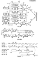
- the range-finding apparatus 10 is shown in block diagram forms in Figure 1, and comprises an accurate and stable high frequency clock oscillator 11, whose output on line 12 is applied to a random binary sequence generator 13. Such generators are well known and may generate the signal by developing zero mean gaussian noise through the use of hot resistors, vacuum tubes, or computers.
- the sequence generator outputs on line 14 comprises a waveform of binary bits in completely random form, such as a NRZI waveform.
- the waveform on line 14 is applied to a mixer 15 to modulate a signal on a line 16 from a local oscillator 17.
- the modulated signal on line 18 is then processed and transmitted via an antenna 19, and, as shown by the signal path 21, is reflected off an object 22 which is being ranged and returns on the path 23 to the receiving antenna 24.
- the processed received signal on line 25 is applied to a code locked loop 26.
- the signal on line 25 is thus the delayed and attenuated transmitted signal from antenna 19.
- the binary bits from the random sequence generator 13 on line 14 are stored cyclically in a predetermined repetitive sequence of addresses in memory 27.
- the stored data is later read from memory 27 and appears on line 28 as an input to a code locked loop 26 to produce a variable frequency clock signal on line 29.
- variable frequency clock signal on line 29 is applied to read address logic 31.
- the sequence of addresses on line 32 from read address logic 31 is applied as a read address pointer to memory 27 to identify the data being read out of memory 27 on line 28.
- the information being read out of memory 27 was previously written into memory 27 via line 14 at the addresses identified by the write address logic 33 via line 34.
- the addresses on line 32 point to the same sequence of addresses as the addresses on line 34, but are delayed in time, as will be explained in greater detail hereinafter.
- the addresses generated by write address logic 33 are being sequentially advanced by the fixed frequency clock 11 via line 12.
- a unique predetermined write address generated on line 34, is recognised by start logic 35 to generate a start signal on line 36 which is applied to range logic 37.
- start logic 35 When the same unique predetermined address is generated by the read address logic 31 on line 32, it is recognised by stop logic 38 and generates a stop signal on line 39 which is applied to the range logic 37.
- stop logic 38 When the same unique predetermined address is generated by the read address logic 31 on line 32, it is recognised by stop logic 38 and generates a stop signal on line 39 which is applied to the range logic 37.
- the time difference between the start signal and the stop signal is in direct proportion to the range from the system 10 to the object 22.
- the decode logic 41 is stepped by the clock input on line 12 to produce an alternating read-write enable signal on line 42.
- the enable signal on line 42 is processed by read-write control logic 43 and determines via line 44 which of the address pointers 34 or 32 are enabled. It will be understood that this output from read-write control logic 43 on line 44 also determines whether the write function or the read function in memory will be performed.
- the data being placed in memory 27 at one fixed location via line 14 is being taken out at a later time at a variable location via line 28.
- the distance between the memory address positions is a measure of the range when the system is locked onto target. As the distance between the object or target 22 and the system 10 is increased, the separation (or time) between the writing position and the reading position is also increased.
- the maximum range that can be measured is reached when the separation between lines 14 and 28 employs all the memory positions of memory 27, so that the maximum range of the system is only limited by the size of the memory 27.
- FIG. 2 shows in greater detail a preferred form of code locked loop 26.
- the signal on line 25 from the receiving antenna 24 is processed in a signal processor 45 and passes to a mixer 46, where it is correlated with a signal from the memory on line 28.
- the mixer output on line 47 is applied to a bandpass filter 48, which gives a signal on line 49 at carrier frequency whose amplitude is indicative of the degree of correlation between the signals on lines 25 and 28.
- An envelope detector 51 removes the carrier and provides a carrier envelope signal on line 52 which is applied to the dither logic 53.
- the dither logic 53 provides an analogue voltage signal on line 54 which directs the voltage controlled oscillator 55 to increase or decrease the frequency.
- the variable output frequency on line 29 allows data to be read out of memory 27 on line 28 such that it maintains the exact alignment or synchronism with the data on line 25.
- FIG. 3 shows in greater detail the operation of the memory 27, which comprises a multiplexer 56 and a random access memory (RAM) chip 57.
- RAM chip 57 has only one set of address inputs for either read or write. The control of read or write is determined by a signal on read-write control line 42 which is applied to the read/write input of chip 57.
- the write enable signals 58 are high for writing as shown in Figure 4 and that the read enable signals 59 are represented by the low portion of the waveform on line 42.
- line 42 When line 42 is high to enable writing, it also enables write address logic 33 and selects the A input of the multiplexer (MUX) 56 so that the write address on line 34 is presented on output line 61 of MUX 56. This allows the data on line 14 to be written into memory 57 at the address on line 61. Only one address is presented on line 61 during the write signal 58.
- signal 58 goes low, as shown at the transition point 62, the write address is sequenced one count by its clock 12 input and then disabled. Now the signal 59 on line 42 is in the low state and the memory 57 is in. the read state. Line 42 is low and selects the B input of MUX 56 so that the address on line 32 is presented to the memory 57 via line 61.
- the data stored in memory 57 at the address designated by the address on line 61 is presented on memory output line 63 to shift register 64. Assume that the line 65 is active and high to enable shift register 64 and read address logic 31. When the next transition point 66 of the clock 11 occurs on line 12, the output of memory 57 on line 63 is clocked into shift register 64 and appears at the QO output of shift register 64 on line 67. The clock transition 66 on line 12 at read address logic 31 advances the address one sequential count so that the new address on line 32 is now presented to memory 57 on line 61. The data in memory 57 at the address designated on line 61 is now presented on memory output line 63.
- the next clock transition point 68 on line 12 at shift register 64 now shifts the data on line 67 to the Q1 output on line 69.
- the same clock transition point 68 shifts the data on line 63 from memory 57 to shift register 64 and is presented on the 00 output line 67.
- the clock transition point 68 also appears at read address logic 31 and sequences the address count on line 32. Further, the clock transition 68 causes sequencer 71 to change the output on line 65 from a high to a low condition.
- variable clock transition point 76 on line 29 causes the data stored in the QO position of shift register 74 to be shifted to the Ql position so that it appears on line 28.
- the same transition 76 also appears at the clock input of flip-flop 73 and causes the Q output on line 72 to go high, thus completing one load and shift cycle.
- the data stored in the addresses of memory 57 designated by the read address 31 may be retrieved and presented on line 28 at a rate determined by the variable frequency clock on line 29.
- the high to low transition of the Q output of flip-flop 73 on line 72 occurs at every other variable frequency clock pulse because flip-flop 73 acts as a divide-by-two logic element.
- the high to low trigger 77 on line 72 is applied to the trigger input of sequencer 71 to indicate that two bits of data from RAM 57 have been accepted by shift register 74.
- transition signal 75 is applied to sequencer 71, the logic of sequencer 71 awaits the next following high to low transition 78 of signal 58 which causes sequencer 71 to go from a high to a low state as shown by the transition 79 on line 65.
- the next following low to high transition 81 of signal 58 causes sequencer 71 to go from high to low as shown by the transition 82 on line 65.
- Memory 57 in its commercial form is not an asynchronous memory, but the memory 57 when coupled with the elements which control shift registers 64 and 74 permit asynchronous read-write operation of the system.
- the fixed oscillator 11, the random sequence generator 13 and state decode logic 41 operate in the same manner previously explained with reference to Figure 1.
- data is written into memory 57 at a fixed rate, and the write addresses are also supplied at line 34 via write address logic 33 at a fixed rate.
- a predetermined unique address which has been designated as a start epoch, appears on line 34 it generates a start signal from start decoder logic 35 on line 36.
- the start signal starts the range logic 37.
- shift register 85 When the same predetermined address is generated by read address logic 31 on line 32, it generates a stop pulse on line 84 which is applied to shift register 85.
- the shift register 85 is enabled and clocked by the same signals which clock and enable shift register 64 on lines 12 and 65.
- the preferred embodiment described above has preferably employed a 1K by 1 read-write RAM memory and is capable of performing range computations up to 50,000 feet when operated at a fixed clock frequency rate of 30 megahertz. In other applications where longer ranging distances are involved, only the memory 57 needs to be enlarged or extended.
- variable frequency clock signal on line 29 and the fixed frequency clock signal on line 12 may be phase-compared in range logic 37.
- the start signal can be produced directly via phantom line 91 to range logic 37, and the need for start decode logic 35 is eliminated.
- the read address on line 32 which produces the stop signal on line 39 could occur at different times depending on the range being detected..
Landscapes
- Engineering & Computer Science (AREA)
- Radar, Positioning & Navigation (AREA)
- Remote Sensing (AREA)
- Computer Networks & Wireless Communication (AREA)
- Physics & Mathematics (AREA)
- General Physics & Mathematics (AREA)
- Radar Systems Or Details Thereof (AREA)
Applications Claiming Priority (2)
| Application Number | Priority Date | Filing Date | Title |
|---|---|---|---|
| US06/256,448 US4429310A (en) | 1981-04-22 | 1981-04-22 | Random binary waveform encoded ranging apparatus |
| US256448 | 1981-04-22 |
Publications (2)
| Publication Number | Publication Date |
|---|---|
| EP0063496A1 true EP0063496A1 (de) | 1982-10-27 |
| EP0063496B1 EP0063496B1 (de) | 1985-10-30 |
Family
ID=22972274
Family Applications (1)
| Application Number | Title | Priority Date | Filing Date |
|---|---|---|---|
| EP82302039A Expired EP0063496B1 (de) | 1981-04-22 | 1982-04-21 | Kodierte Signale aussendender Entfernungsmesser |
Country Status (5)
| Country | Link |
|---|---|
| US (1) | US4429310A (de) |
| EP (1) | EP0063496B1 (de) |
| JP (1) | JPS57182670A (de) |
| CA (1) | CA1176356A (de) |
| DE (1) | DE3267109D1 (de) |
Cited By (4)
| Publication number | Priority date | Publication date | Assignee | Title |
|---|---|---|---|---|
| EP0156375A2 (de) * | 1984-03-30 | 1985-10-02 | Honeywell Inc. | Pulssynchronisationseinrichtung |
| EP0362992A2 (de) * | 1988-10-06 | 1990-04-11 | Nkk Corporation | Verfahren zur Entfernungsmessung und Gerät dafür |
| EP0449590A2 (de) * | 1990-03-30 | 1991-10-02 | Nkk Corporation | Gerät zum Messen des Schlackenniveaus in einem Ofen |
| GB2273409A (en) * | 1992-12-10 | 1994-06-15 | Marconi Gec Ltd | Distance measuring arrangement |
Families Citing this family (9)
| Publication number | Priority date | Publication date | Assignee | Title |
|---|---|---|---|---|
| US5825387A (en) * | 1995-04-27 | 1998-10-20 | Hewlett-Packard Company | Ink supply for an ink-jet printer |
| US6947471B1 (en) * | 1998-01-05 | 2005-09-20 | Intel Corporation | Method for using encoded spreading codes to achieve high bit densities in a direct-sequence spread spectrum communication system |
| GB2353155A (en) * | 1999-08-05 | 2001-02-14 | Mitsubishi Electric Inf Tech | A random binary signal generator with a narrowed autocorrelation function |
| US6407697B1 (en) | 2000-06-15 | 2002-06-18 | Honeywell International Inc. | Low probability of intercept coherent radar altimeter |
| DE10208618A1 (de) * | 2002-02-27 | 2003-09-04 | Bosch Gmbh Robert | Digitale Verzögerungsleitung |
| US6731234B1 (en) * | 2003-06-11 | 2004-05-04 | Honeywell International Inc. | Radar anti-fade systems and methods |
| US7064703B2 (en) * | 2004-02-17 | 2006-06-20 | Honeywell International Inc. | Methods and apparatus for randomly modulating radar altimeters |
| DE602007005937D1 (de) * | 2007-06-11 | 2010-05-27 | Mitsubishi Electric Corp | Objekterkennung |
| WO2013090568A1 (en) | 2011-12-15 | 2013-06-20 | Northrop Grumman Guidance And Electronics Company, Inc. | System and method for detection of rf signal spoofing |
Citations (2)
| Publication number | Priority date | Publication date | Assignee | Title |
|---|---|---|---|---|
| DE2133497B2 (de) * | 1971-07-06 | 1974-04-18 | Honeywell Gmbh, 6000 Frankfurt | |
| EP0049150A1 (de) * | 1980-09-29 | 1982-04-07 | Sperry Corporation | Radarsender und -empfänger für ein breites Spektrum |
-
1981
- 1981-04-22 US US06/256,448 patent/US4429310A/en not_active Expired - Fee Related
-
1982
- 1982-04-19 CA CA000401187A patent/CA1176356A/en not_active Expired
- 1982-04-21 DE DE8282302039T patent/DE3267109D1/de not_active Expired
- 1982-04-21 EP EP82302039A patent/EP0063496B1/de not_active Expired
- 1982-04-22 JP JP57066417A patent/JPS57182670A/ja active Pending
Patent Citations (2)
| Publication number | Priority date | Publication date | Assignee | Title |
|---|---|---|---|---|
| DE2133497B2 (de) * | 1971-07-06 | 1974-04-18 | Honeywell Gmbh, 6000 Frankfurt | |
| EP0049150A1 (de) * | 1980-09-29 | 1982-04-07 | Sperry Corporation | Radarsender und -empfänger für ein breites Spektrum |
Non-Patent Citations (1)
| Title |
|---|
| IEEE TRANSACTIONS ON AEROSPACE AND ELECTRONIC SYSTEMS, Vol. AES-15, No. 1, January 1979, New York, D.F. ALBANESE et al.: "Pseudorandom Code Waveform Design for CW Radar" pages 67 to 75 * |
Cited By (7)
| Publication number | Priority date | Publication date | Assignee | Title |
|---|---|---|---|---|
| EP0156375A2 (de) * | 1984-03-30 | 1985-10-02 | Honeywell Inc. | Pulssynchronisationseinrichtung |
| EP0156375A3 (en) * | 1984-03-30 | 1987-05-06 | Honeywell Inc. | Pulse synchronizing apparatus |
| EP0362992A2 (de) * | 1988-10-06 | 1990-04-11 | Nkk Corporation | Verfahren zur Entfernungsmessung und Gerät dafür |
| EP0362992A3 (de) * | 1988-10-06 | 1992-07-29 | Nkk Corporation | Verfahren zur Entfernungsmessung und Gerät dafür |
| EP0449590A2 (de) * | 1990-03-30 | 1991-10-02 | Nkk Corporation | Gerät zum Messen des Schlackenniveaus in einem Ofen |
| EP0449590A3 (en) * | 1990-03-30 | 1992-11-19 | Nkk Corporation | In-furnace slag level measuring apparatus |
| GB2273409A (en) * | 1992-12-10 | 1994-06-15 | Marconi Gec Ltd | Distance measuring arrangement |
Also Published As
| Publication number | Publication date |
|---|---|
| EP0063496B1 (de) | 1985-10-30 |
| DE3267109D1 (en) | 1985-12-05 |
| CA1176356A (en) | 1984-10-16 |
| JPS57182670A (en) | 1982-11-10 |
| US4429310A (en) | 1984-01-31 |
Similar Documents
| Publication | Publication Date | Title |
|---|---|---|
| EP0063496B1 (de) | Kodierte Signale aussendender Entfernungsmesser | |
| US4106019A (en) | Range resolving doppler radar system | |
| US4038540A (en) | Quadrature correlation pulse detector | |
| US6278397B1 (en) | Quiet radar method and apparatus | |
| US5184135A (en) | Phase measurement of received pseudonoise sequence using digital correlation | |
| US5285472A (en) | System for determining the acquisition of, and frequency compensating, a phase modulated pseudonoise sequence signal | |
| US3530470A (en) | Radio ranging system | |
| EP0131260B1 (de) | Anordnung zur Anzeige der genauen Ankunftszeit eines empfangenen Signals | |
| US4860318A (en) | PSK detection using an IFM receiver | |
| US3887918A (en) | Multi-level digital coincidence detection | |
| AU608491B2 (en) | Digital system for codeless phase measurement | |
| US4071821A (en) | Quadrature correlation phase determining apparatus | |
| US3175214A (en) | Doppler-free distance measuring system | |
| US5293168A (en) | Radar apparatus and method | |
| US4513285A (en) | Quasi coherent two-way ranging apparatus | |
| US3391344A (en) | Digital signal synchronous detector with noise blanking means | |
| US4569078A (en) | Image sensor | |
| US3947845A (en) | Altitude coding for collision avoidance system | |
| KR100905338B1 (ko) | 디지털 신호 상관 방법, 컴퓨터 판독 가능한 저장 매체, 전자 디바이스 및 gps 수신기 | |
| US5144639A (en) | Spread-spectrum communication system | |
| US5347645A (en) | Time code interface | |
| RU2076333C1 (ru) | Дальномерная система с измерением фазы радиосигнала | |
| US3199105A (en) | Distance measuring systems | |
| RU2073880C1 (ru) | Пеленгатор | |
| RU2118054C1 (ru) | Приемник спутниковых радионавигационных систем |
Legal Events
| Date | Code | Title | Description |
|---|---|---|---|
| PUAI | Public reference made under article 153(3) epc to a published international application that has entered the european phase |
Free format text: ORIGINAL CODE: 0009012 |
|
| AK | Designated contracting states |
Designated state(s): DE FR GB |
|
| 17P | Request for examination filed |
Effective date: 19821206 |
|
| GRAA | (expected) grant |
Free format text: ORIGINAL CODE: 0009210 |
|
| AK | Designated contracting states |
Designated state(s): DE FR GB |
|
| REF | Corresponds to: |
Ref document number: 3267109 Country of ref document: DE Date of ref document: 19851205 |
|
| ET | Fr: translation filed | ||
| PLBE | No opposition filed within time limit |
Free format text: ORIGINAL CODE: 0009261 |
|
| STAA | Information on the status of an ep patent application or granted ep patent |
Free format text: STATUS: NO OPPOSITION FILED WITHIN TIME LIMIT |
|
| 26N | No opposition filed | ||
| PGFP | Annual fee paid to national office [announced via postgrant information from national office to epo] |
Ref country code: FR Payment date: 19920410 Year of fee payment: 11 |
|
| PGFP | Annual fee paid to national office [announced via postgrant information from national office to epo] |
Ref country code: GB Payment date: 19930319 Year of fee payment: 12 |
|
| PGFP | Annual fee paid to national office [announced via postgrant information from national office to epo] |
Ref country code: DE Payment date: 19930428 Year of fee payment: 12 |
|
| PG25 | Lapsed in a contracting state [announced via postgrant information from national office to epo] |
Ref country code: FR Effective date: 19931229 |
|
| REG | Reference to a national code |
Ref country code: FR Ref legal event code: ST |
|
| PG25 | Lapsed in a contracting state [announced via postgrant information from national office to epo] |
Ref country code: GB Effective date: 19940421 |
|
| GBPC | Gb: european patent ceased through non-payment of renewal fee |
Effective date: 19940421 |
|
| PG25 | Lapsed in a contracting state [announced via postgrant information from national office to epo] |
Ref country code: DE Effective date: 19950103 |