EP0060882B1 - Electrical connector - Google Patents
Electrical connector Download PDFInfo
- Publication number
- EP0060882B1 EP0060882B1 EP81902789A EP81902789A EP0060882B1 EP 0060882 B1 EP0060882 B1 EP 0060882B1 EP 81902789 A EP81902789 A EP 81902789A EP 81902789 A EP81902789 A EP 81902789A EP 0060882 B1 EP0060882 B1 EP 0060882B1
- Authority
- EP
- European Patent Office
- Prior art keywords
- lever
- circuit board
- printed circuit
- electrical connector
- pin
- Prior art date
- Legal status (The legal status is an assumption and is not a legal conclusion. Google has not performed a legal analysis and makes no representation as to the accuracy of the status listed.)
- Expired
Links
Images


Classifications
-
- H—ELECTRICITY
- H01—ELECTRIC ELEMENTS
- H01R—ELECTRICALLY-CONDUCTIVE CONNECTIONS; STRUCTURAL ASSOCIATIONS OF A PLURALITY OF MUTUALLY-INSULATED ELECTRICAL CONNECTING ELEMENTS; COUPLING DEVICES; CURRENT COLLECTORS
- H01R12/00—Structural associations of a plurality of mutually-insulated electrical connecting elements, specially adapted for printed circuits, e.g. printed circuit boards [PCB], flat or ribbon cables, or like generally planar structures, e.g. terminal strips, terminal blocks; Coupling devices specially adapted for printed circuits, flat or ribbon cables, or like generally planar structures; Terminals specially adapted for contact with, or insertion into, printed circuits, flat or ribbon cables, or like generally planar structures
- H01R12/70—Coupling devices
- H01R12/82—Coupling devices connected with low or zero insertion force
- H01R12/85—Coupling devices connected with low or zero insertion force contact pressure producing means, contacts activated after insertion of printed circuits or like structures
- H01R12/87—Coupling devices connected with low or zero insertion force contact pressure producing means, contacts activated after insertion of printed circuits or like structures acting automatically by insertion of rigid printed or like structures
-
- H—ELECTRICITY
- H01—ELECTRIC ELEMENTS
- H01R—ELECTRICALLY-CONDUCTIVE CONNECTIONS; STRUCTURAL ASSOCIATIONS OF A PLURALITY OF MUTUALLY-INSULATED ELECTRICAL CONNECTING ELEMENTS; COUPLING DEVICES; CURRENT COLLECTORS
- H01R4/00—Electrically-conductive connections between two or more conductive members in direct contact, i.e. touching one another; Means for effecting or maintaining such contact; Electrically-conductive connections having two or more spaced connecting locations for conductors and using contact members penetrating insulation
- H01R4/26—Connections in which at least one of the connecting parts has projections which bite into or engage the other connecting part in order to improve the contact
-
- H—ELECTRICITY
- H01—ELECTRIC ELEMENTS
- H01R—ELECTRICALLY-CONDUCTIVE CONNECTIONS; STRUCTURAL ASSOCIATIONS OF A PLURALITY OF MUTUALLY-INSULATED ELECTRICAL CONNECTING ELEMENTS; COUPLING DEVICES; CURRENT COLLECTORS
- H01R4/00—Electrically-conductive connections between two or more conductive members in direct contact, i.e. touching one another; Means for effecting or maintaining such contact; Electrically-conductive connections having two or more spaced connecting locations for conductors and using contact members penetrating insulation
- H01R4/28—Clamped connections, spring connections
- H01R4/50—Clamped connections, spring connections utilising a cam, wedge, cone or ball also combined with a screw
- H01R4/5008—Clamped connections, spring connections utilising a cam, wedge, cone or ball also combined with a screw using rotatable cam
Definitions
- This invention relates to an electrical connector for a printed circuit board having an edge contact, said connector including an electrically conductive pin, and movable interconnection means including an electrically conductive member having first and second ends adapted to make contact with said edge contact and said pin at respective first and second contact points.
- resilient contact members are normally strongly biased towards each other, that is, towards the printed circuit board being inserted into the connector.
- the resulting mechanical biasing force serves two purposes, the first being to provide the electrical connections and the second being to grip the printed circuit board, and thus hold the board in the connector.
- the biasing force exerted by the resilient members must be relatively high to insure that good conductive contacts are made and maintained.
- the high biasing force causes a high insertion force of the PCB or the like which becomes excessive when the number of the interconnection elements of the connector is of a large quantity, the problem of the high insertion force being the impetus behind the development of zero insertion force and low insertion force connectors.
- an electrical connector of the kind specified characterized in that said pin is resiliently deflectable by said electrically conductive member, and in that said electrically conductive member is formed by a lever mounted in a rotatable carrier of electrically insulating material, said lever having ends of a sharpened configuration, the arrangement being such that on insertion into said connector said printed circuit board engages said carrier thereby initiating a rotary movement of said lever to bring said first end thereof into engagement with said edge contact at said first contact point, continued rotary movement of said lever causing said pin to be deflected, whereby the sharpened ends of said lever are maintained in engagement with said edge contact and said pin at said first and second contact points respectively.
- Fig. 1 is a partial exploded section view of the total connector assembly and Fig. 2 is an end-view cross-section of the connector 1 without the printed circuit board or the like inserted.
- the connector housing comprising a top wall 10, a front wall 11, a back wall 12, two side walls 13 (one is shown in Fig. 1) having a groove 33 for guiding the insertion of a printed circuit board, and a base 14, is shown which is made of an electrically insulative material.
- the walls and base of the connector housing form a hollow cavity 17 within the connector 1.
- Top wall 10 has an opening 15 for permitting the insertion of a printed circuit board (PCB) 16 or the like into the connector 1, the PCB 16 having edge contacts or terminal strips 26.
- PCB printed circuit board
- two rows of pins 18 are permanently fixed in the base 14 and extend a length 19 outside the connector housing through the base 14 and into the cavity 17.
- the two rows are on opposite sides of a base centerline 10 and equidistant therefrom, the base centerline 20 being on the base surface and parallel to the front wall 11 and the back wall 12.
- the pins 18 are spaced apart equally within the row. It will be recognized by those skilled in the art that many alternative configurations may be divised including, a single pin, a single row of pins, or a row or rows of pins not spaced apart equally.
- each pin 18 there is an electrically conductive lever 21 for each pin 18 providing the interconnection between the edge contact 26 and the pin 18, each lever 21 being partially encased in a lever carrier 22, or simply referred to herein as a carrier 22, made of an electrically insulative material, with both ends of the lever 21 extending outside the carrier 22 and both ends having a sharp point or edge.
- a lever carrier 22 or simply referred to herein as a carrier 22, made of an electrically insulative material, with both ends of the lever 21 extending outside the carrier 22 and both ends having a sharp point or edge.
- Each pin 18 extends far enough into the cavity 17 such that the corresponding lever 21 always maintains pin contact.
- Two carriers 22 are positioned within cavity 17, such that the levers can rotate in a plane substantially perpendicular to the base centerline 20.
- the pin 18 is capable of being deflected as a cantilever beam when a force is applied, the cantilever beam action to be described hereinunder. In the ready state, i.e.
- the two carriers 22 are held in position by the force exerted by the pins 18.
- the pins 18 in the ready state are slightly deflected causing the two carrier surfaces 24 to press against one another, thereby holding carriers 22 in equilibrium between the pins 18.
- the sharp edges of the levers 21 hold the levers 21 at a fixed point on the pins 18.
- a notch 25 can be placed in pin 18 to insure the lever 21/pin 18 position is maintained, the notch 25 being configured so as not to interfere with lever 21 rotation.
- the other end of the lever 21 is just outside opening 15 and may be in contact with the inside surface of top wall 10.
- the carrier 22 is so shaped that it doesn't interfere with the lever 21/pin 18 contact during any lever 21 rotation, the rotation of the lever 21 will be described in detail hereinunder.
- the carrier 22 is further shaped such that a portion of the carrier 22 extends in the path taken by the PCB 16 during insertion.
- the levers 21, pins 18, and edge contacts 26 may be made of an electrically conductive noble or non-noble metal. Again it will be recognized by those skilled in the art that, although the preferred embodiment shows the ends of the lever 21 having a chisel-like end configuration, the ends of the lever 21 may be configured to many different shapes while providing a good contact point with the pin 18 and the edge contact 26 respectively, the shapes including pointed, square edged, conical, and the like.
- Fig. 2 shows the connector 1 in the ready state.
- the levers 21 are in the position as mentioned above such that the PCB 16 can travel beyond the edges of levers 21 to the point depicted by PCB 16' where initial contact is made with carriers 22, the carriers 22 being shaped such that a portion extends in the path of travel of PCB 16 as mentioned above.
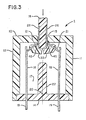
- Fig. 3 shows the connector 1 in which the PCB 16 has travelled a sufficient distance to cause rotation of the carriers 22 such that the edges of the levers 21, which were shown initially resting upon the inner surface of top wall 10, are making contact at contact points 45 with their corresponding edge contacts 26 (or terminal strips) of PCB 16. Such rotation also causes a force against pins 18 by lever 21, thereby initiating a deflection of pins 18 from the initial or ready state.
- the leading edge of PCB 16 continues to push against carriers 22, and together with the contact point 45 made between levers 21 and edge contacts 26, the carriers 22 are rotated further, the initial contact points 45 being maintained throughout insertion of PCB 16 by the knife-like action of the sharp edges of levers 21.
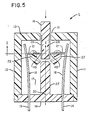
- Figs. 4 and 5 show interim positions of PCB travel during insertion and Fig. 6 shows the PCB 16 fully inserted, the PCB 16 travel being stopped by a block 27. It will be recognized by those skilled in the art that alternative means may be included for stopping the PCB 16 travel, including a step 34 in groove 33 (reference Fig. 1).
- Fig. 5 shows the levers 21 having rotated perpendicular to the PCB 16 causing the maximum deflection of pins 18. From a lever position beyond the perpendicular to the PCB 16, there exists a small component of force along the PCB 16 travel path which results in a latching action of the PCB 16. This arrangement has the advantage that the PCB 16 is pulled or snapped in, i.e.
- the person inserting the board is made aware of complete insertion by sensing or observing the snapping-in action, and the board is held positively in place by the inward force component.
- the force required for insertion is that force required to overcome the small force component along the PCB travel path. It can be seen that the sharp points or edges at each end of the levers along with a high contact force caused by pin 18 deflection permits an action which pierces non-noble metallic oxides thus allowing good electrical connections. It will be understood by those skilled in the art that the piercing action of the non-noble metallic oxides includes actions such as friction, rubbing, knifing, cutting, etc., achieved by the lever 21 ends having alternative configurations mentioned above.
- Figs. 7A and 7B are a cross-sectional view of a partial connector 1 taken along section line I-I of Fig. 5.
- Fig. 7A shows levers 21A through 21D mounted in carrier 22 and by some error, shows lever 21A extending farther out of carrier 22 than levers 21B, 21C, and 21D on the side making contact with PCB 16.
- lever 21A has created a high-spot thereby preventing levers 21 B, 21 C and 21 D from making any contact with their corresponding edge contacts 26.
- Pins 18A to 18D press against their respective levers 21A to 21D, pin 18A being the only pin benefitting from the cantilever action.
- the levers 21 can be loosely fitted into the carrier 22, permitting the lever 21 to travel along its length, as indicated by the arrows of Fig. 7B, within the carrier 22. In this manner the lever 21 is responsive to the cantilever action of its respective pin 18 nullifying the effect of the high-spot.
- each lever 21 is mounted in its own individual carrier 41, as shown in Fig. 8.
- the lever 21 may be affixed within carrier 41 since the levers 21 will not be subjected to a high-spot, each lever 21 being free to rotate independent of the other.
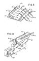
- Figs. 9 and 10 show an alternative embodiment which includes fins 52 which is part of the carrier 22, the fins 52 being formed on the carrier 22 along the carrier length for every few pins.
- the fins 52 are configured complementary to each other such that the carriers 22 may close as shown in Fig. 2, and such that the carriers 22 may be fully opened as shown in Fig. 6 without interfering with pins 18.
- a slot 51 is made in block 27 to permit the carriers 22 to open unimpeded, the slot 51 placement corresponding to the placement of the fins 52.
- the fins 52 are utilized to assist in holding the alignment of the carriers 22 such that the axis of rotation of the carriers 22 remains parallel to the base centerline.
Description
- This invention relates to an electrical connector for a printed circuit board having an edge contact, said connector including an electrically conductive pin, and movable interconnection means including an electrically conductive member having first and second ends adapted to make contact with said edge contact and said pin at respective first and second contact points.
- In one known type of printed circuit board connector, resilient contact members are normally strongly biased towards each other, that is, towards the printed circuit board being inserted into the connector. The resulting mechanical biasing force serves two purposes, the first being to provide the electrical connections and the second being to grip the printed circuit board, and thus hold the board in the connector. It should be apparent that the biasing force exerted by the resilient members must be relatively high to insure that good conductive contacts are made and maintained. The high biasing force causes a high insertion force of the PCB or the like which becomes excessive when the number of the interconnection elements of the connector is of a large quantity, the problem of the high insertion force being the impetus behind the development of zero insertion force and low insertion force connectors.
- Another problem with these connectors is that the contact areas of the edge contacts and the interconnecting elements will rub against each other with considerable force during insertion and removal of the printed circuit board or the like. Since the edge contacts of a typical printed circuit board are only a few thousandths of an inch thick, this rubbing action which occurs during insertion and removal of the printed circuit board tends to wear away the edge contacts and may well ruin a PCB after several insertions and removals. This rubbing action may also wear away high-cost precious metal on the surface of the interconnecting elements which invites poor electrical contacts or corrosion and can result in hard to detect failures of the equipment.
- Attempts have been made to overcome these problems, for example the low insertion force connector disclosed in U.S. Patent No. 3,478,301. When a printed circuit board is inserted into this known connector, the board engages levers which move to cause cam surfaces to bring resilient, outwardly biased contact members towards and into engagement with printed circuit board contact terminals. During the initial stage of insertion the contact members do not engage the board contact terminals, but during the final stage of the insertion of the board into the connector there is a wiping action between convex surfaces on the contact members and the associated conductive surfaces of the terminals, which wiping action serves to break through the oxide coating which forms on the terminals. This known connector has the disadvantage that for this wiping action to be effective in breaking through the oxide coating an unduly high insertion force is needed at least during the portion of the circuit board insertion operation when wiping action is taking place.
- From the document DE-A-2 423 266 there is known an electrical connector of the kind specified hereinabove, wherein an electrically conductive terminal is fixed on an insulator body. Cooperating with the terminal is a contact spring having a nose at one end located in an aperture in a slide, the other end serving as a pivot point when the insertion of a printed circuit board produces sliding movement of the slide. As a result of such insertion, the spring is compressed until the nose abuts against the corresponding contact strip of the printed circuit board. This construction has the disadvantage of being complex, especially in view of the separate slide member, and the further disadvantage of additional functional constraints introduced by the movement of the slide member.
- According to the present invention, there is provided an electrical connector of the kind specified, characterized in that said pin is resiliently deflectable by said electrically conductive member, and in that said electrically conductive member is formed by a lever mounted in a rotatable carrier of electrically insulating material, said lever having ends of a sharpened configuration, the arrangement being such that on insertion into said connector said printed circuit board engages said carrier thereby initiating a rotary movement of said lever to bring said first end thereof into engagement with said edge contact at said first contact point, continued rotary movement of said lever causing said pin to be deflected, whereby the sharpened ends of said lever are maintained in engagement with said edge contact and said pin at said first and second contact points respectively.
- It will be appreciated that in an electrical connector according to the invention the maintenance of the ends of the electrically conductive member in contact with the first and second contact points by the deflected pins enables a high contact force to be produced which is capable of piercing any oxide coating, together with a relatively low insertion force as compared with the insertion force needed for a wiping action to break through any oxide coating.
- It will be appreciated that it is an advantage of an electrical connector according to the invention that good electrical contacts can be achieved despite the use of non-noble metals for the contacts.
- Embodiments of the invention will now be described by way of example with reference to the accompanying drawings, in which:
- Fig. 1 is an exploded partial section view of an electrical connector assembly;
- Fig. 2 is an end-view cross-section of the connector assembly of Fig. 1 taken along the section line II-II without the printed circuit board inserted;
- Fig. 2A is a magnified view of the encircled contact point of Fig. 2;
- Fig. 3 is the end-view cross-section of the Fig. 2 connector with the printed circuit board partially inserted;
- Fig. 4 is the end-view cross-section of the Fig. 2 connector with the printed circuit board inserted further than shown in Fig. 3;
- Fig. 5 is the end-view cross-section of the Fig. 2 connector with the printed circuit board inserted further than shown in Fig. 4;
- Fig. 6 is the end-view cross-section of the Fig. 2 connector with the printed circuit board fully inserted;
- Figs. 7A and 7B are a cross-sectional view of a partial connector taken along section line I-I of Fig. 5;
- Fig. 8 shows an alternative embodiment of the carriers;
- Fig. 9 is an end-view cross-section of the connector with another alternative embodiment of the carriers showing alignment fins; and
- Fig. 10 is a perspective view of the alternative embodiment of the carriers of Fig. 9.
- The construction of the
preferred embodiment connector 1 of the present invention is shown in Figs. 1 and 2. Fig. 1 is a partial exploded section view of the total connector assembly and Fig. 2 is an end-view cross-section of theconnector 1 without the printed circuit board or the like inserted. Referring to Figs. 1 and 2, the connector housing, comprising atop wall 10, a front wall 11, aback wall 12, two side walls 13 (one is shown in Fig. 1) having agroove 33 for guiding the insertion of a printed circuit board, and abase 14, is shown which is made of an electrically insulative material. The walls and base of the connector housing form ahollow cavity 17 within theconnector 1.Top wall 10 has anopening 15 for permitting the insertion of a printed circuit board (PCB) 16 or the like into theconnector 1, thePCB 16 having edge contacts orterminal strips 26. - In the preferred embodiment, two rows of
pins 18 are permanently fixed in thebase 14 and extend alength 19 outside the connector housing through thebase 14 and into thecavity 17. The two rows are on opposite sides of abase centerline 10 and equidistant therefrom, thebase centerline 20 being on the base surface and parallel to the front wall 11 and theback wall 12. Thepins 18 are spaced apart equally within the row. It will be recognized by those skilled in the art that many alternative configurations may be divised including, a single pin, a single row of pins, or a row or rows of pins not spaced apart equally. - There is an electrically
conductive lever 21 for eachpin 18 providing the interconnection between theedge contact 26 and thepin 18, eachlever 21 being partially encased in alever carrier 22, or simply referred to herein as acarrier 22, made of an electrically insulative material, with both ends of thelever 21 extending outside thecarrier 22 and both ends having a sharp point or edge. Eachpin 18 extends far enough into thecavity 17 such that thecorresponding lever 21 always maintains pin contact. Twocarriers 22 are positioned withincavity 17, such that the levers can rotate in a plane substantially perpendicular to thebase centerline 20. Thepin 18 is capable of being deflected as a cantilever beam when a force is applied, the cantilever beam action to be described hereinunder. In the ready state, i.e. a condition in which the connector is ready for thePCB 16 or the like insertion, the twocarriers 22 are held in position by the force exerted by thepins 18. Thepins 18 in the ready state are slightly deflected causing the twocarrier surfaces 24 to press against one another, thereby holdingcarriers 22 in equilibrium between thepins 18. The sharp edges of thelevers 21 hold thelevers 21 at a fixed point on thepins 18. As shown in Fig. 2A, anotch 25 can be placed inpin 18 to insure thelever 21/pin 18 position is maintained, thenotch 25 being configured so as not to interfere withlever 21 rotation. The other end of thelever 21 is just outside opening 15 and may be in contact with the inside surface oftop wall 10. Thecarrier 22 is so shaped that it doesn't interfere with thelever 21/pin 18 contact during anylever 21 rotation, the rotation of thelever 21 will be described in detail hereinunder. Thecarrier 22 is further shaped such that a portion of thecarrier 22 extends in the path taken by thePCB 16 during insertion. Thelevers 21,pins 18, andedge contacts 26 may be made of an electrically conductive noble or non-noble metal. Again it will be recognized by those skilled in the art that, although the preferred embodiment shows the ends of thelever 21 having a chisel-like end configuration, the ends of thelever 21 may be configured to many different shapes while providing a good contact point with thepin 18 and theedge contact 26 respectively, the shapes including pointed, square edged, conical, and the like. - Fig. 2 shows the
connector 1 in the ready state. Thelevers 21 are in the position as mentioned above such that the PCB 16 can travel beyond the edges oflevers 21 to the point depicted by PCB 16' where initial contact is made withcarriers 22, thecarriers 22 being shaped such that a portion extends in the path of travel of PCB 16 as mentioned above. - Fig. 3 shows the
connector 1 in which thePCB 16 has travelled a sufficient distance to cause rotation of thecarriers 22 such that the edges of thelevers 21, which were shown initially resting upon the inner surface oftop wall 10, are making contact atcontact points 45 with their corresponding edge contacts 26 (or terminal strips) ofPCB 16. Such rotation also causes a force againstpins 18 bylever 21, thereby initiating a deflection ofpins 18 from the initial or ready state. AsPCB 16 is further inserted intoconnector 1, the leading edge ofPCB 16 continues to push againstcarriers 22, and together with thecontact point 45 made betweenlevers 21 andedge contacts 26, thecarriers 22 are rotated further, the initial contact points 45 being maintained throughout insertion ofPCB 16 by the knife-like action of the sharp edges oflevers 21. - Figs. 4 and 5 show interim positions of PCB travel during insertion and Fig. 6 shows the
PCB 16 fully inserted, thePCB 16 travel being stopped by ablock 27. It will be recognized by those skilled in the art that alternative means may be included for stopping thePCB 16 travel, including astep 34 in groove 33 (reference Fig. 1). Fig. 5 shows thelevers 21 having rotated perpendicular to thePCB 16 causing the maximum deflection ofpins 18. From a lever position beyond the perpendicular to thePCB 16, there exists a small component of force along thePCB 16 travel path which results in a latching action of thePCB 16. This arrangement has the advantage that thePCB 16 is pulled or snapped in, i.e. there is a negative insertion force at this time, ensuring complete insertion. Furthermore, the person inserting the board is made aware of complete insertion by sensing or observing the snapping-in action, and the board is held positively in place by the inward force component. The force required for insertion is that force required to overcome the small force component along the PCB travel path. It can be seen that the sharp points or edges at each end of the levers along with a high contact force caused bypin 18 deflection permits an action which pierces non-noble metallic oxides thus allowing good electrical connections. It will be understood by those skilled in the art that the piercing action of the non-noble metallic oxides includes actions such as friction, rubbing, knifing, cutting, etc., achieved by thelever 21 ends having alternative configurations mentioned above. - Figs. 7A and 7B are a cross-sectional view of a
partial connector 1 taken along section line I-I of Fig. 5. Fig. 7A showslevers 21A through 21D mounted incarrier 22 and by some error, showslever 21A extending farther out ofcarrier 22 thanlevers PCB 16. In such case,lever 21A has created a high-spot thereby preventinglevers corresponding edge contacts 26.Pins 18A to 18D press against theirrespective levers 21A to 21D, pin 18A being the only pin benefitting from the cantilever action. In an alternative embodiment, in order to correct for the error or to compensate for manufacturing tolerances, thelevers 21 can be loosely fitted into thecarrier 22, permitting thelever 21 to travel along its length, as indicated by the arrows of Fig. 7B, within thecarrier 22. In this manner thelever 21 is responsive to the cantilever action of itsrespective pin 18 nullifying the effect of the high-spot. - In yet another embodiment, each
lever 21 is mounted in its ownindividual carrier 41, as shown in Fig. 8. In this embodiment, thelever 21 may be affixed withincarrier 41 since thelevers 21 will not be subjected to a high-spot, eachlever 21 being free to rotate independent of the other. - Figs. 9 and 10 show an alternative embodiment which includes
fins 52 which is part of thecarrier 22, thefins 52 being formed on thecarrier 22 along the carrier length for every few pins. Thefins 52 are configured complementary to each other such that thecarriers 22 may close as shown in Fig. 2, and such that thecarriers 22 may be fully opened as shown in Fig. 6 without interfering withpins 18. Aslot 51 is made inblock 27 to permit thecarriers 22 to open unimpeded, theslot 51 placement corresponding to the placement of thefins 52. Thefins 52 are utilized to assist in holding the alignment of thecarriers 22 such that the axis of rotation of thecarriers 22 remains parallel to the base centerline.
Claims (8)
Priority Applications (1)
| Application Number | Priority Date | Filing Date | Title |
|---|---|---|---|
| AT81902789T ATE14641T1 (en) | 1980-10-06 | 1981-09-18 | ELECTRICAL CONNECTOR. |
Applications Claiming Priority (2)
| Application Number | Priority Date | Filing Date | Title |
|---|---|---|---|
| US06/194,491 US4355856A (en) | 1980-10-06 | 1980-10-06 | Low insertion force connector using non-noble metal contact plating |
| US194491 | 1980-10-06 |
Publications (3)
| Publication Number | Publication Date |
|---|---|
| EP0060882A1 EP0060882A1 (en) | 1982-09-29 |
| EP0060882A4 EP0060882A4 (en) | 1983-04-18 |
| EP0060882B1 true EP0060882B1 (en) | 1985-07-31 |
Family
ID=22717803
Family Applications (1)
| Application Number | Title | Priority Date | Filing Date |
|---|---|---|---|
| EP81902789A Expired EP0060882B1 (en) | 1980-10-06 | 1981-09-18 | Electrical connector |
Country Status (9)
| Country | Link |
|---|---|
| US (1) | US4355856A (en) |
| EP (1) | EP0060882B1 (en) |
| JP (1) | JPS57501556A (en) |
| AU (1) | AU545096B2 (en) |
| BE (1) | BE890632A (en) |
| CA (1) | CA1159529A (en) |
| DK (1) | DK252182A (en) |
| WO (1) | WO1982001280A1 (en) |
| ZA (1) | ZA816408B (en) |
Families Citing this family (18)
| Publication number | Priority date | Publication date | Assignee | Title |
|---|---|---|---|---|
| US4448466A (en) * | 1981-11-12 | 1984-05-15 | Ncr Corporation | Low insertion force connector for printed circuit boards |
| US4488766A (en) * | 1982-09-30 | 1984-12-18 | Amp Incorporated | High density zero insertion force connector |
| US4522456A (en) * | 1984-01-25 | 1985-06-11 | Datakey, Inc. | Electronic tag receptacle and reader |
| GB8521843D0 (en) * | 1985-09-03 | 1985-10-09 | Bicc Plc | Circuit board connector |
| US4700998A (en) * | 1986-08-19 | 1987-10-20 | Northern Telecom Limited | Multiple contact connector having a low insertion force |
| JPH0424625Y2 (en) * | 1987-11-11 | 1992-06-10 | ||
| US6483329B1 (en) * | 2000-08-28 | 2002-11-19 | Micron Technology, Inc. | Test system, test contactor, and test method for electronic modules |
| US6489794B1 (en) * | 2000-08-31 | 2002-12-03 | Micron Technology, Inc. | High speed pass through test system and test method for electronic modules |
| US6993392B2 (en) * | 2002-03-14 | 2006-01-31 | Duke University | Miniaturized high-density multichannel electrode array for long-term neuronal recordings |
| WO2009029864A1 (en) * | 2007-08-29 | 2009-03-05 | Datakey Electronics, Inc. | Data carrier system and method |
| USD649894S1 (en) | 2008-12-30 | 2011-12-06 | Atek Products, Llc | Electronic token and data carrier |
| USD649895S1 (en) | 2009-01-30 | 2011-12-06 | Atek Products, Llc | Electronic token and data carrier |
| WO2010088556A1 (en) | 2009-01-30 | 2010-08-05 | Datakey Electronics, Inc. | Data carrier system having a compact footprint and methods of manufacturing the same |
| USD649896S1 (en) | 2009-01-30 | 2011-12-06 | Atek Products, Llc | Electronic token and data carrier receptacle |
| USD649486S1 (en) | 2009-07-09 | 2011-11-29 | ATEK Products , LLC | Electronic token and data carrier |
| EP3299832B1 (en) * | 2016-09-23 | 2018-12-19 | Siemens Healthcare GmbH | Local coil with a first connecting element of a connector, and magnetic resonance apparatus or patient table with a corresponding second connecting element |
| US10587060B2 (en) | 2017-11-30 | 2020-03-10 | International Business Machines Corporation | Electrical contacts on the sidewall of a circuit board |
| US11189949B2 (en) * | 2019-10-10 | 2021-11-30 | Rolls-Royce Corporation | Electrical connection devices for high power applications |
Citations (1)
| Publication number | Priority date | Publication date | Assignee | Title |
|---|---|---|---|---|
| JPS4422981B1 (en) * | 1966-04-04 | 1969-09-30 |
Family Cites Families (7)
| Publication number | Priority date | Publication date | Assignee | Title |
|---|---|---|---|---|
| US2825037A (en) * | 1955-02-04 | 1958-02-25 | Harry H French | Printed-circuit card clamp |
| US2920163A (en) * | 1956-11-13 | 1960-01-05 | William J Johnson | Electrical connector for building panels |
| US3478301A (en) * | 1967-04-06 | 1969-11-11 | Itt | Low insertion force cam-actuated printed circuit board connector |
| SU493946A1 (en) * | 1972-03-03 | 1975-11-28 | Предприятие П/Я В-8657 | Contact device |
| FR2230150B1 (en) * | 1973-05-18 | 1975-08-22 | Socapex | |
| US4118094A (en) * | 1977-03-31 | 1978-10-03 | Trw Inc. | Zero-entry force connector |
| SU639056A1 (en) * | 1977-08-18 | 1978-12-25 | Предприятие П/Я В-2203 | Plug-and-socket connector |
-
1980
- 1980-10-06 US US06/194,491 patent/US4355856A/en not_active Expired - Lifetime
-
1981
- 1981-09-15 ZA ZA816408A patent/ZA816408B/en unknown
- 1981-09-16 CA CA000386040A patent/CA1159529A/en not_active Expired
- 1981-09-18 JP JP56503253A patent/JPS57501556A/ja active Pending
- 1981-09-18 AU AU76498/81A patent/AU545096B2/en not_active Ceased
- 1981-09-18 EP EP81902789A patent/EP0060882B1/en not_active Expired
- 1981-09-18 WO PCT/US1981/001279 patent/WO1982001280A1/en active IP Right Grant
- 1981-10-05 BE BE0/206170A patent/BE890632A/en not_active IP Right Cessation
-
1982
- 1982-06-04 DK DK252182A patent/DK252182A/en not_active Application Discontinuation
Patent Citations (1)
| Publication number | Priority date | Publication date | Assignee | Title |
|---|---|---|---|---|
| JPS4422981B1 (en) * | 1966-04-04 | 1969-09-30 |
Also Published As
| Publication number | Publication date |
|---|---|
| DK252182A (en) | 1982-06-04 |
| AU7649881A (en) | 1982-04-28 |
| JPS57501556A (en) | 1982-08-26 |
| AU545096B2 (en) | 1985-06-27 |
| EP0060882A1 (en) | 1982-09-29 |
| US4355856A (en) | 1982-10-26 |
| ZA816408B (en) | 1982-09-29 |
| BE890632A (en) | 1982-02-01 |
| EP0060882A4 (en) | 1983-04-18 |
| CA1159529A (en) | 1983-12-27 |
| WO1982001280A1 (en) | 1982-04-15 |
Similar Documents
| Publication | Publication Date | Title |
|---|---|---|
| EP0060882B1 (en) | Electrical connector | |
| EP0093167B1 (en) | Electrical connector | |
| US3173737A (en) | Connector with tab terminal latching means | |
| CA1118063A (en) | Electrical terminal and a circuit board edge connector comprising such terminals | |
| US5564952A (en) | Electrical plug connector with blade receiving slots | |
| US4978315A (en) | Multiple-conductor electrical connector and stamped and formed contacts for use therewith | |
| US5411408A (en) | Electrical connector for printed circuit boards | |
| US3553630A (en) | Low insertion force connector | |
| US4713020A (en) | Connector unit | |
| US4637670A (en) | Dual in-line package carrier assembly | |
| EP1791220A1 (en) | High speed card edge connector | |
| US3478301A (en) | Low insertion force cam-actuated printed circuit board connector | |
| US4270826A (en) | Zero insertion force connector | |
| US4474420A (en) | Electrical connector for flexible printed circuits | |
| AU591635B2 (en) | Electrical connector | |
| US5775938A (en) | Connector for flat cables | |
| US5921785A (en) | Electrical connector for flat cables | |
| US3990761A (en) | Zero force connector assembly | |
| KR930000792Y1 (en) | Connector | |
| KR960001306Y1 (en) | Law insertion force connector and electrical contact therefor | |
| US4752246A (en) | Preloaded spring contact electrical terminal | |
| EP0065357B1 (en) | Low insertion force connector | |
| US3421136A (en) | Electrical contact and edge connector having such a contact | |
| US3876278A (en) | Fuse holder contact | |
| US4869685A (en) | Electrical connector having terminals with positive retention means and improved mating zones |
Legal Events
| Date | Code | Title | Description |
|---|---|---|---|
| PUAI | Public reference made under article 153(3) epc to a published international application that has entered the european phase |
Free format text: ORIGINAL CODE: 0009012 |
|
| AK | Designated contracting states |
Designated state(s): AT CH DE FR GB NL |
|
| 17P | Request for examination filed |
Effective date: 19820918 |
|
| DET | De: translation of patent claims | ||
| TCAT | At: translation of patent claims filed | ||
| GRAA | (expected) grant |
Free format text: ORIGINAL CODE: 0009210 |
|
| AK | Designated contracting states |
Designated state(s): AT CH DE FR GB LI NL |
|
| REF | Corresponds to: |
Ref document number: 14641 Country of ref document: AT Date of ref document: 19850815 Kind code of ref document: T |
|
| REF | Corresponds to: |
Ref document number: 3171596 Country of ref document: DE Date of ref document: 19850905 |
|
| ET | Fr: translation filed | ||
| PLBE | No opposition filed within time limit |
Free format text: ORIGINAL CODE: 0009261 |
|
| STAA | Information on the status of an ep patent application or granted ep patent |
Free format text: STATUS: NO OPPOSITION FILED WITHIN TIME LIMIT |
|
| 26N | No opposition filed | ||
| PGFP | Annual fee paid to national office [announced via postgrant information from national office to epo] |
Ref country code: AT Payment date: 19860903 Year of fee payment: 6 |
|
| PGFP | Annual fee paid to national office [announced via postgrant information from national office to epo] |
Ref country code: NL Payment date: 19870930 Year of fee payment: 7 |
|
| PG25 | Lapsed in a contracting state [announced via postgrant information from national office to epo] |
Ref country code: GB Effective date: 19880918 Ref country code: AT Effective date: 19880918 |
|
| PG25 | Lapsed in a contracting state [announced via postgrant information from national office to epo] |
Ref country code: LI Effective date: 19880930 Ref country code: CH Effective date: 19880930 |
|
| PG25 | Lapsed in a contracting state [announced via postgrant information from national office to epo] |
Ref country code: NL Effective date: 19890401 |
|
| NLV4 | Nl: lapsed or anulled due to non-payment of the annual fee | ||
| PG25 | Lapsed in a contracting state [announced via postgrant information from national office to epo] |
Ref country code: FR Free format text: LAPSE BECAUSE OF NON-PAYMENT OF DUE FEES Effective date: 19890531 |
|
| REG | Reference to a national code |
Ref country code: CH Ref legal event code: PL |
|
| GBPC | Gb: european patent ceased through non-payment of renewal fee | ||
| PG25 | Lapsed in a contracting state [announced via postgrant information from national office to epo] |
Ref country code: DE Effective date: 19890601 |
|
| REG | Reference to a national code |
Ref country code: FR Ref legal event code: ST |