EP0057616A1 - Starting and operating apparatus for fluorescent lamps - Google Patents
Starting and operating apparatus for fluorescent lamps Download PDFInfo
- Publication number
- EP0057616A1 EP0057616A1 EP82300575A EP82300575A EP0057616A1 EP 0057616 A1 EP0057616 A1 EP 0057616A1 EP 82300575 A EP82300575 A EP 82300575A EP 82300575 A EP82300575 A EP 82300575A EP 0057616 A1 EP0057616 A1 EP 0057616A1
- Authority
- EP
- European Patent Office
- Prior art keywords
- lamp
- circuit
- transformer
- primary winding
- capacitor
- Prior art date
- Legal status (The legal status is an assumption and is not a legal conclusion. Google has not performed a legal analysis and makes no representation as to the accuracy of the status listed.)
- Granted
Links
Images


Classifications
-
- H—ELECTRICITY
- H05—ELECTRIC TECHNIQUES NOT OTHERWISE PROVIDED FOR
- H05B—ELECTRIC HEATING; ELECTRIC LIGHT SOURCES NOT OTHERWISE PROVIDED FOR; CIRCUIT ARRANGEMENTS FOR ELECTRIC LIGHT SOURCES, IN GENERAL
- H05B41/00—Circuit arrangements or apparatus for igniting or operating discharge lamps
- H05B41/14—Circuit arrangements
- H05B41/26—Circuit arrangements in which the lamp is fed by power derived from dc by means of a converter, e.g. by high-voltage dc
- H05B41/28—Circuit arrangements in which the lamp is fed by power derived from dc by means of a converter, e.g. by high-voltage dc using static converters
- H05B41/295—Circuit arrangements in which the lamp is fed by power derived from dc by means of a converter, e.g. by high-voltage dc using static converters with semiconductor devices and specially adapted for lamps with preheating electrodes, e.g. for fluorescent lamps
-
- Y—GENERAL TAGGING OF NEW TECHNOLOGICAL DEVELOPMENTS; GENERAL TAGGING OF CROSS-SECTIONAL TECHNOLOGIES SPANNING OVER SEVERAL SECTIONS OF THE IPC; TECHNICAL SUBJECTS COVERED BY FORMER USPC CROSS-REFERENCE ART COLLECTIONS [XRACs] AND DIGESTS
- Y02—TECHNOLOGIES OR APPLICATIONS FOR MITIGATION OR ADAPTATION AGAINST CLIMATE CHANGE
- Y02B—CLIMATE CHANGE MITIGATION TECHNOLOGIES RELATED TO BUILDINGS, e.g. HOUSING, HOUSE APPLIANCES OR RELATED END-USER APPLICATIONS
- Y02B20/00—Energy efficient lighting technologies, e.g. halogen lamps or gas discharge lamps
-
- Y—GENERAL TAGGING OF NEW TECHNOLOGICAL DEVELOPMENTS; GENERAL TAGGING OF CROSS-SECTIONAL TECHNOLOGIES SPANNING OVER SEVERAL SECTIONS OF THE IPC; TECHNICAL SUBJECTS COVERED BY FORMER USPC CROSS-REFERENCE ART COLLECTIONS [XRACs] AND DIGESTS
- Y10—TECHNICAL SUBJECTS COVERED BY FORMER USPC
- Y10S—TECHNICAL SUBJECTS COVERED BY FORMER USPC CROSS-REFERENCE ART COLLECTIONS [XRACs] AND DIGESTS
- Y10S315/00—Electric lamp and discharge devices: systems
- Y10S315/04—Dimming circuit for fluorescent lamps
-
- Y—GENERAL TAGGING OF NEW TECHNOLOGICAL DEVELOPMENTS; GENERAL TAGGING OF CROSS-SECTIONAL TECHNOLOGIES SPANNING OVER SEVERAL SECTIONS OF THE IPC; TECHNICAL SUBJECTS COVERED BY FORMER USPC CROSS-REFERENCE ART COLLECTIONS [XRACs] AND DIGESTS
- Y10—TECHNICAL SUBJECTS COVERED BY FORMER USPC
- Y10S—TECHNICAL SUBJECTS COVERED BY FORMER USPC CROSS-REFERENCE ART COLLECTIONS [XRACs] AND DIGESTS
- Y10S315/00—Electric lamp and discharge devices: systems
- Y10S315/07—Starting and control circuits for gas discharge lamp using transistors
Definitions
- This invention relates to starting and operating apparatus for fluorescent lamps and, more particularly, to a transistorized inverter apparatus for starting and operating compact fluorescent lamps.
- Transistorized inverter circuits for operating fluorescent lamps from a DC power supply are well known, a typical circuit being disclosed in U.S. Patent No. 3,593,060. Such circuits normally operate the lamps at a relatively high frequency above the audible range which enhances the efficiency of operation. In addition, such circuits can be made relatively light as compared to the more usual inductive reactor ballast.
- U.S. Patent No. 3,579,026 discloses a transistorized inverter ballast in which a capacitor and transformer provide a tank circuit for the oscillations of the inverter.
- U.S. Patent No. 3,371,244 is disclosed a transistorized inverter circuit for operating a discharge device in which a parallelling capacitor is connected across the output winding of the inverter with an additional capacitor in series with the lamp.
- the parallelling capacitor is stated to serve the purpose of reducing spike voltages reflected across the transistors and the series capacitor is described as included in order to improve the power factor of the circuit.
- the present invention resides in a starting and operating apparatus for a fluorescent lamp having a sealed elongated light-transmitting envelope with electrodes operatively positioned therein proximate the ends thereof and enclosing a discharge-sustaining filling and having phosphor means coated on the envelope interior surface, said apparatus comprising:
- the specific lamp 10 as shown in Fig. 1 forms no part of the present invention; however, the present apparatus is particularly adapted to operate such a lamp.
- the lamp 10 comprises an elongated light-transmitting envelope 12 with electrodes 14 operatively positioned within the envelope 12 proximate the ends thereof and enclosing a discharge-sustaining filling such as a small charge of mercury 16.
- a layer of phosphor means 18 is coated onto the interior surface of the envelope 12.
- a base member 20 is affixed to the ends of the envelope 12 and the electrodes 14 connect via lead-in members 22 to base pins 24.
- the envelope 12 is provided with a double-folded configuration with the overall "unfolded" length of the envelope 12 being approximately 16 inches (40.6 cm).
- the envelope outer diameter is approximately 0.75 inch (1.9 cm) and the envelope contains a small charge of inert, ionizable starting gas, such as a few torr of argon.
- the phosphor layer 18 preferably comprises a three component blend of rare-earth activated materials such as disclosed in U.S. Patent No. 3,937,998, dated February 10, 1976 to Verstegen et al. Other conventional phosphors may be substituted therefor.
- the phosphor blend is provided with a warm-white source color (approximately 3,000°K) so that it appears generally similar to the incandescent lamp which it is intended to replace.
- a lamp unit 26 is shown in Fig. 2 wherein the lamp 10 is mounted on a platform member 28 which has affixed thereto a decorative type housing 30 which terminates in a conventional incandescent-type base 32.
- the folded lamp 10 is preferably partially enclosed within a transparent or translucent casing 34 in order to provide protection and for purposes of appearance. Ventilating slots 36 are provided in the housing member 30 and additional slots 38 are provided in the top portion of casing 34.
- the apparatus of the present invention is contained within the housing 30 and is preferably mounted on the bottom portion of platform 28.
- the lamp 10 can either be permanently affixed to the platform 28 or it can be made with a plug-in design, such as shown in Fig. 1, in order that the electronic ballast apparatus can be used with a replacement lamp.
- the apparatus 40 comprises a pair of input terminals 42a, 42b adapted to be connected across a household-type source of AC energizing potential (120V AC, 60 Hz), and a pair of apparatus output terminals 44a, 44b across which the lamp 10 to be operated is adapted to be connected.
- An AC to DC conversion apparatus 46 preferably comprises a full-wave rectifier bridge 48 having rectifier input terminals 50a, 50b and rectifier output terminals 52a, 52b.
- Current limiting impedance means R1 is included in circuit with the rectifier bridge 48 in order to limit the current therethrough.
- a storage capacitor C 1 has one terminal 54a connected to the positive output terminal 52a of the rectifier bridge 48 and the other terminal 54b connects through chassis ground to the other output terminal 52b of the rectifier bridge 48.
- a transformer means T1 has a primary winding T p of predetermined inductance and a secondary winding T .
- the transformer primary winding T p is connected at its midpoint 56 to the more positive output terminal 54a of the storage capacitor C 1 via a choke L 1 which constitutes a high impedance at the operating frequencies of the circuit.
- a tuned circuit capacitor C 2 of predetermined capacitance connects across the transformer primary winding T .
- a current limiting capacitor C 3 of predetermined capacitance and the apparatus output terminals 44a, 44b are connected in series, with the series-connected current limiting capacitor C 3 and the apparatus output terminals 44a, 44b connected in parallel with the tuned circuit capacitor C 2 .
- a pair of separate transistor means Q 1 , Q 2 each has a collector 58a, 58b and emitter 60a, 60b and a base 62a, 62b.
- the collectors 58a, 58b of the transistors are respectively connected to opposite ends 64a, 64b of the transformer primary winding T .
- the respective emitters 60a, 60b of the transistors connect to the less positive terminal 54b of the storage capacitor C 1 via a common electrical point, i.e., chassis ground.
- the bases 62a, 62b of the transistors respectively connect to the ends 66a, 66b of the transformer secondary winding T .
- the transformer secondary winding T s is connected at its midpoint 68 with the common electrical point, i.e., chassis ground, in series with means for blocking direct current flow toward the common electrical point, which in this case is a blocking diode D 1 .
- the midpoint terminal 68 of transformer secondary T s connects to the more positive terminal 54a of the storage capacitor means C 1 through a resistor R 2 in order to provide a positive potential to initiate transistor conduction upon energization of the apparatus 40.
- a resistor R 3 and inductor L 2 of predetermined values are connected in series between the cathode of the blocking diode D 1 and the midpoint connection 68 of the transformer secondary winding T in order to optimize the switching current delivered to the bases of the transistors Q 1 , Q 2'
- the lamp 10 has a pair of lead-in members 22 sealed through each end thereof and connecting to the respective lamp electrodes 14 (see Fig. 1).
- a small electrode preheating current is applied therethrough prior to the low pressure discharge being initiated between the respective electrodes.
- This preheat current is provided by preheating coils 70 and 72 provided on the core of transformer T 1 with the respective connections between the heater coils and electrodes shown as x-x, and y-y.
- the rectifier 48 charges storage capacitor C 1 to the peak value of the AC voltage input and for a 120V AC supply, this will be approximately 170V DC.
- the transistors Q 1 and Q 2 are put into a conducting mode via the common base resistor R 2 .
- the tuned circuit across which the collectors 58a, 58b are connected consists of the transformer primary T p and tuned circuit capacitor C 2 and this tuned circuit is coupled to the transistor base circuits via the secondary T s of transformer T 1 to provide positive feedback.
- the loop gain of the circuit is sufficient to cause self-sustaining oscillations to occur.
- the lamp 10 essentially acts as an open circuit element so that oscillations occur at a frequency determined by the inductance of the transformer primary (Lp) and the capacitance of C2.
- the voltage developed across T 1 is approximately 377V rms and almost all of this voltage is applied across the lamp 10. This causes the lamp to strike and operation of same is initiated.
- the lamp operating characteristics are shown in Fig. 4 wherein the striking voltage V s and the lamp operating voltage V L are plotted on the ordinate and the lamp current I L is plotted on the abscissa.
- the circuit maintains the 377V rms across transformer T 1 and the current through the lamp is determined by the capacitive reactance of C 3 and the lamp impedance.
- the lamp impedance R L is almost entirely resistive at the frequencies of operation considered, hence the voltage across C 3 (V C3 ) and the lamp voltage (V L ) can be determined from the vector diagram shown in Fig. 5.
- the desired lamp current can be achieved.
- the voltage drop across C 3 is much larger than the voltage drop across the lamp and good ballast stabilization of lamp current is achieved.
- the frequency of oscillations is determined by the inductance of the transformer primary T and the capacitance of the tuned circuit capacitor C 2 and a typical initial "lamp starting" resonant frequency is approximately 77 kHz.
- the resonant frequency of operation is determined by the inductance of the transformer primary (L ) and the capacitance of C 2 and C 3 such that:
- the operating frequency can be calculated as approximately 50 kHz which provides a good compromise between transistor switching losses and component sizes.
- FIGS. 6A through 6E show the voltage-current timing relationships that occur at various parts of the foregoing apparatus.
- the circuit operates in Class D and it will be observed that the voltages at the collectors of the transistors are minimum (in saturation) when the collector currents are flowing and hence, minimum dissipation occurs in the transistors.
- the voltage drops across Q 1 and Q 2 are indicated as V Q1 and V Q2 in Fig. 3 and Figs. 6A and 6C and typically have a peak value of 534 V.
- the currents through Q 1 and Q 2 are indicated as I Q1 and I Q2 in Figs. 3 and Figs. 6B and 6D and typically have a value of 160 mA for a lamp operated with a light output of 1500 lumens.
- the voltage across L 1 is indicated as V L1 in Fig. 3 and Fig. 6E and typically has a peak value of 267V.
- Inductor L 1 provides a direct current path and also acts as a high impedance choke at the operating frequency of the circuit. Due to the push-pull nature of the conduction of the transistors, the voltage across L 1 looks like a full wave voltage rectification at the operating frequency, as shown in Fig. 6(E) which does not contain the fundamental component of the frequency. Thus the junction of L 1 and the midpoint 56 of the primary of T is a null point at the operating frequency.
- the power input to the system is approximately 27 watts so that the system efficacy is approximately 55 lumens per watt.
- the circuit is approximately 90% efficient so that under these conditions of operation, the wattage losses in the circuit are approximately 2.7 watts.
- the system operates with a power factor of approximately 0.6.
- the lamp current is approximately 0.45 A rms.
- the current limiting capacitor C 3 has substituted therefore two capacitors each having one-half the value of capacitance of the capacitor C 3 .
- One of these capacitors designated aC 3/ 2 connects directly in series with the lamp 10 to be operated and the other capacitor bC 3/ 2 is connected in series with a two position switch 74.
- the two capacitors aC 3/ 2 and bC 3/ 2 are connected in parallel and in series with the lamp 10 as operated.
- the capacitor bC 3/ 2 will be connected in parallel with the capacitor C 2 and in parallel with the series-connected capacitor aC 3/ 2 and the operating lamp 10.
- the value of the current limiting capacitive reactance will be twice the value of the corresponding reactance when the switch is in the other position 78.
- the resulting lamp brightness can thus be set for one of two predetermined values, one of which is twice the other. Equally important, however, whichever position the switch 74 occupies, the total capacitive reactance in the tuned circuit will always remain the same so that the circuit operation is not altered by varying the brightness of the lamp.
- the resonant frequency during starting will be modified somewhat, depending upon the position of the switch 68, but this is a very transient condition and does not affect the lamp operation.
- the lamp unit 26 as shown in Fig. 2 can be readily modified to incorporate the additional switch 74 by locating it at the exterior edge of the platform 28, for example. The user can then select that level of light which is desired.
- the circuit as diagrammed in Fig. 3 can be modified by the substitution of PNP transistors for the NPN transistors as shown in Fig. 9 with the polarity of the diodes being reversed. Other than this, the two circuits are identical.
- the transformer T 1 is connected at the midpoint of the primary winding T p via the choke L 1 to one output terminal of the AC to DC conversion means 48.
- the transistors remain connected in push-pull arrangement between the ends of the transformer primary winding T and the other output terminal of the AC to DC conversion means 48.
- Fig. 10 is shown a graph of lamp starting voltage V (rms) vs. lamp electrode heater current I h (rms) for the particular compact fluorescent lamp as described hereinbefore.
- V (rms) lamp electrode heater current
- I h lamp electrode heater current
- the starting voltage requirement essentially remains independent of heater current.
- the heater currents can be decreased or even reduced to zero with negligible effect on the lamp operation.
- actuation of only one heater is required for effective starting and will result in a starting voltage requirement which is not significantly different from that of a lamp which has two electrode heaters activated, provided the minimum electrode heating current is exceeded.
- Fig. 11 is shown an alternative circuit embodiment wherein only one lamp electrode 14a is heated.
- the voltage developed across T 1 is approximately constant at 377 V rms both during start-up and operation of the lamp.
- the operating frequency is approximately 50 kHz and before the lamp strikes, the resonant frequency for this embodiment can be calculated as:
- the current through C 2 and hence the current through the electrode coil or heater 14a is calculated by the voltage across the transformer primary T divided by the reactance of capacitor C 2 . This is equal to 377 x 2 ⁇ fsC l which equals 0.34 ampere. For this particular lamp, this is greater than the minimum heater current required, as shown in Fig. 10, and start-up is achieved.
- the operating frequency drops to 50 kHz and the current through C 2 and thus through the heater is reduced to V 2 ⁇ f r C 2 which can be calculated as 0.19 ampere.
- This reduction in heater current results in a reduction of heater power and hence improves the system efficacy.
- the power saved due to non-activation of the second electrode 14b also results in improved system efficacy.
- the transformer electrode heater coils 70 and 72 are eliminated, and the ends of the uppermost electrode 14b are tied together.
- the electrode 14a which is heated is connected in electrical circuit intermediate one end 64b of the transformer primary winding T and the tuned circuit capacitor C 2 , in order to effect electrode preheating.
- an additional capacitor C 4 is desirably connected across the heated electrode 14a in order to short circuit high-voltage pulses which may occur if the electrode 14a has an open circuit, in order to prevent damage to the transistors.
- the additional capacitor C 4 can typically have a value of 0.02 microfarad so that it essentially has no affect on the operation of the circuit.
- the tuned circuit capacitor means C 2 is connected in series with the lamp electrode 14a when the lamp 10 is connected in circuit across the output terminals 44a, 44b, 44c of the apparatus.
- the series-connected tuned circuit capacitor means C 2 and the lamp electrode 14a are thus connected across the ends 64a, 64b of the transformer primary winding T p to form therewith a first resonant tuned circuit when the lamp is not operating, which as previously described has a resonant frequency of approximately 90 kHz.
- a current limiting capacitor means C 3 is connected in series with the lamp 10 as connected in circuit, with the series-connected lamp and the current limiting capacitor means C 3 connected in parallel with the tuned circuit capacitor means C 2 .
- the current limiting capacitor means C 3 and the tuned circuit capacitor means C 2 form with the transformer means primary winding T a second tuned circuit when the lamp is connected in circuit and is operating, with the frequency of the second tuned circuit being approximately 50 kHz.
- the other identified elements of the circuit of Fig. 11 are as shown in Fig. 3 and described hereinbefore.
- Fig. 12 is shown yet another alternative circuit wherein only one of the electrodes 14a of the lamp 10 is adapted to be preheated to facilitate starting.
- the electrode 14a is connected in electrical circuit intermediate one of the transistors Q 2 and one end 64b of the transformer means primary winding T p in order to effect electrode preheating.
- the current through the electrode before the lamp starts can be calculated as V c /X Lp which is equal to 377/2 ⁇ f s L p and during running, the heater current can be calculated as V C /2 ⁇ f R L p .
- the heater current can be calculated as 0.43 ampere, which is greater than the minimum heater current required to facilitate starting and the operating heater current can be calculated as 0.667 ampere.
- the transformer primary winding T p and the lamp electrode 14a are connected in series when the lamp is connected across the apparatus output terminals.
- the tuned circuit capacitor means C 2 is connected in parallel with the series-connected transformer primary T p and the lamp electrode 14a in order to form a first resonant tuned circuit when the lamp 10 is not operating.
- a current limiting capacitor C3 connects in series with the lamp 10 as connected in circuit and the series-connected lamp 10 and the current limiting capacitor C 3 connect in parallel with the tuned circuit capacitor C 2 .
- the current limiting capacitor C 3 and the tuned circuit capacitor C 2 form with the transformer primary T p a second tuned circuit when the lamp 10 is actually operating.
- the other identified elements of the circuit of Fig. 12 are as shown in Fig. 3 and described hereinbefore.
- the PNP transistors can be substituted for the NPN transistors.
- any of the foregoing embodiments can be modified to provide a predetermined degree of dimming, in the manner as described for the circuits as shown in Figs. 7 and 8.
Abstract
Description
- This invention relates to starting and operating apparatus for fluorescent lamps and, more particularly, to a transistorized inverter apparatus for starting and operating compact fluorescent lamps.
- Transistorized inverter circuits for operating fluorescent lamps from a DC power supply are well known, a typical circuit being disclosed in U.S. Patent No. 3,593,060. Such circuits normally operate the lamps at a relatively high frequency above the audible range which enhances the efficiency of operation. In addition, such circuits can be made relatively light as compared to the more usual inductive reactor ballast.
- U.S. Patent No. 3,579,026 (Paget) discloses a transistorized inverter ballast in which a capacitor and transformer provide a tank circuit for the oscillations of the inverter.
- In U.S. Patent No. 3,371,244 is disclosed a transistorized inverter circuit for operating a discharge device in which a parallelling capacitor is connected across the output winding of the inverter with an additional capacitor in series with the lamp. The parallelling capacitor is stated to serve the purpose of reducing spike voltages reflected across the transistors and the series capacitor is described as included in order to improve the power factor of the circuit.
- Accordingly, the present invention resides in a starting and operating apparatus for a fluorescent lamp having a sealed elongated light-transmitting envelope with electrodes operatively positioned therein proximate the ends thereof and enclosing a discharge-sustaining filling and having phosphor means coated on the envelope interior surface, said apparatus comprising:
- apparatus input terminals adapted to be connected across a household-type source of AC energizing potential, and apparatus output terminals across which the lamp to be operated is adapted to be connected in circuit;
- AC to DC conversion means having input terminals and output terminals, said conversion means input terminals connected to said apparatus input terminals and said conversion means operable to convert said AC potential to predetermined DC potential which is developed across said conversion means output terminals;
- transformer means having a primary winding of predetermined inductance and a secondary winding, said transformer means primary winding connected at its midpoint via a choke to one output terminal of said conversion means, tuned circuit capacitor means of predetermined capacitance connected across said transformer means primary winding to form therewith a first resonant tuned circuit when said lamp is connected in circuit but is not operating, a current-limiting capacitor means connected in series with said lamp as connected in circuit, said series-connected lamp and current-limiting capacitor means connected in parallel with said tuned circuit capacitor means, and said current-limiting capacitor means and said tuned circuit capacitor means forming with said transformer means primary winding a second tuned circuit when said lamp is connected in circuit and is operating; and
- a pair of transistors connected in push-pull arrangement in circuit between the ends of said transformer means primary winding and the other output terminal of said conversion means when said lamp is connected in circuit, the base members of said transistors connecting across said transformer means secondary winding so that the push-pull connected transistors oscillate at the tuned circuit resonant frequency as determined by the inductance of said transformer means primary winding and the total capacitance of said connected capacitor means, and means for applying a potential from said one output terminal of said conversion means to the midpoint of said transformer means secondary winding to initiate transistor conduction upon energization of said apparatus.
- In order that the invention can be more clearly understood, convenient embodiments thereof will now be described by way of example, with reference to the accompanying drawings in which:
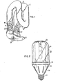
- Fig. 1 is an isometric view, shown partly in section, of a folded-envelope, compact fluorescent lamp;
- Fig. 2 is an elevational view of an operating lamp unit which incorporates the lamp as shown in Fig. 1 and which is intended to be utilized as an incandescent lamp replacement;
- Fig. 3 is a circuit diagram of one embodiment of the present transistorized inverter apparatus;
- Fig. 4 is a graph of voltage versus current showing typical lamp starting and operating characteristics;
- Fig. 5 is a vector diagram of the voltages across the current limiting capacitor, the transformer primary, and the operating lamp;
- Figs. 6A through 6E illustrate voltage and current waveforms which are present in various portions of the circuit as shown in Fig. 3;
- Fig. 7 is a diagram of a portion of the circuit shown in Fig. 3, but showing an alternative embodiment whereby the brightness level of the operating lamp can be adjusted;
- Fig. 8 corresponds to Fig. 7 but illustrates another alternative embodiment wherein relative operating lamp brightness values can be readily predetermined;
- Fig. 9 is a circuit diagram of an alternative embodiment of the circuit as shown in Fig. 3, wherein PNP transistors are used to replace the NPN transistors;
- Fig. 10 is a graph of lamp starting voltage vs. lamp heater voltage for a particular lamp;
- Fig. 11 is an alternative circuit diagram wherein only one lamp electrode is heated during lamp starting and operation; and
- Fig. 12 is another alternative circuit diagram wherein only one lamp electrode is heated during lamp starting and operation.
- The
specific lamp 10 as shown in Fig. 1 forms no part of the present invention; however, the present apparatus is particularly adapted to operate such a lamp. Thelamp 10 comprises an elongated light-transmittingenvelope 12 withelectrodes 14 operatively positioned within theenvelope 12 proximate the ends thereof and enclosing a discharge-sustaining filling such as a small charge ofmercury 16. A layer of phosphor means 18 is coated onto the interior surface of theenvelope 12. Abase member 20 is affixed to the ends of theenvelope 12 and theelectrodes 14 connect via lead-inmembers 22 tobase pins 24. - Considering the
lamp 10 in greater detail, theenvelope 12 is provided with a double-folded configuration with the overall "unfolded" length of theenvelope 12 being approximately 16 inches (40.6 cm). The envelope outer diameter is approximately 0.75 inch (1.9 cm) and the envelope contains a small charge of inert, ionizable starting gas, such as a few torr of argon. For the lamp loadings which are utilized, as will be explained hereinafter, the phosphor layer 18 preferably comprises a three component blend of rare-earth activated materials such as disclosed in U.S. Patent No. 3,937,998, dated February 10, 1976 to Verstegen et al. Other conventional phosphors may be substituted therefor. In its preferred form, the phosphor blend is provided with a warm-white source color (approximately 3,000°K) so that it appears generally similar to the incandescent lamp which it is intended to replace. - A
lamp unit 26 is shown in Fig. 2 wherein thelamp 10 is mounted on aplatform member 28 which has affixed thereto adecorative type housing 30 which terminates in a conventional incandescent-type base 32. The foldedlamp 10 is preferably partially enclosed within a transparent or translucent casing 34 in order to provide protection and for purposes of appearance.Ventilating slots 36 are provided in thehousing member 30 andadditional slots 38 are provided in the top portion of casing 34. The apparatus of the present invention is contained within thehousing 30 and is preferably mounted on the bottom portion ofplatform 28. Thelamp 10 can either be permanently affixed to theplatform 28 or it can be made with a plug-in design, such as shown in Fig. 1, in order that the electronic ballast apparatus can be used with a replacement lamp. - One embodiment of the electronic starting and operating apparatus of the present invention is shown schematically in Fig. 3. The
apparatus 40 comprises a pair ofinput terminals 42a, 42b adapted to be connected across a household-type source of AC energizing potential (120V AC, 60 Hz), and a pair ofapparatus output terminals lamp 10 to be operated is adapted to be connected. - An AC to
DC conversion apparatus 46 preferably comprises a full-wave rectifier bridge 48 havingrectifier input terminals rectifier output terminals rectifier bridge 48 in order to limit the current therethrough. A storage capacitor C1 has oneterminal 54a connected to thepositive output terminal 52a of therectifier bridge 48 and theother terminal 54b connects through chassis ground to theother output terminal 52b of therectifier bridge 48. - A transformer means T1 has a primary winding Tp of predetermined inductance and a secondary winding T . The transformer primary winding Tp is connected at its
midpoint 56 to the morepositive output terminal 54a of the storage capacitor C1 via a choke L1 which constitutes a high impedance at the operating frequencies of the circuit. A tuned circuit capacitor C2 of predetermined capacitance connects across the transformer primary winding T . A current limiting capacitor C3 of predetermined capacitance and theapparatus output terminals apparatus output terminals - A pair of separate transistor means Q1, Q2 each has a
collector emitter base 62a, 62b. Thecollectors opposite ends 64a, 64b of the transformer primary winding T . Therespective emitters positive terminal 54b of the storage capacitor C1 via a common electrical point, i.e., chassis ground. Thebases 62a, 62b of the transistors respectively connect to theends 66a, 66b of the transformer secondary winding T . - The transformer secondary winding Ts is connected at its
midpoint 68 with the common electrical point, i.e., chassis ground, in series with means for blocking direct current flow toward the common electrical point, which in this case is a blocking diode D1. Themidpoint terminal 68 of transformer secondary T s connects to the morepositive terminal 54a of the storage capacitor means C1 through a resistor R2 in order to provide a positive potential to initiate transistor conduction upon energization of theapparatus 40. - To complete the description of the apparatus, a resistor R3 and inductor L2 of predetermined values are connected in series between the cathode of the blocking diode D1 and the
midpoint connection 68 of the transformer secondary winding T in order to optimize the switching current delivered to the bases of the transistors Q1, Q2' - In its preferred form, the
lamp 10 has a pair of lead-inmembers 22 sealed through each end thereof and connecting to the respective lamp electrodes 14 (see Fig. 1). In the usual operation of such lamps, a small electrode preheating current is applied therethrough prior to the low pressure discharge being initiated between the respective electrodes. This preheat current is provided by preheatingcoils 70 and 72 provided on the core of transformer T1 with the respective connections between the heater coils and electrodes shown as x-x, and y-y. - In the operation of the apparatus, upon initial energization, the
rectifier 48 charges storage capacitor C1 to the peak value of the AC voltage input and for a 120V AC supply, this will be approximately 170V DC. The transistors Q1 and Q2 are put into a conducting mode via the common base resistor R2. The tuned circuit across which thecollectors - Initially the
lamp 10 essentially acts as an open circuit element so that oscillations occur at a frequency determined by the inductance of the transformer primary (Lp) and the capacitance of C2. The voltage developed across T1 is approximately 377V rms and almost all of this voltage is applied across thelamp 10. This causes the lamp to strike and operation of same is initiated. The lamp operating characteristics are shown in Fig. 4 wherein the striking voltage Vs and the lamp operating voltage VL are plotted on the ordinate and the lamp current IL is plotted on the abscissa. - The circuit maintains the 377V rms across transformer T1 and the current through the lamp is determined by the capacitive reactance of C3 and the lamp impedance. The lamp impedance RL is almost entirely resistive at the frequencies of operation considered, hence the voltage across C 3(VC3) and the lamp voltage (VL) can be determined from the vector diagram shown in Fig. 5. The current that will flow through the lamp can then be calculated to be approximately:
IL =VC3 27TfC 3 - Thus by selection of the capacitance of C3, the desired lamp current can be achieved. In practice, the voltage drop across C3 is much larger than the voltage drop across the lamp and good ballast stabilization of lamp current is achieved.
- When the apparatus is initially energized, the frequency of oscillations is determined by the inductance of the transformer primary T and the capacitance of the tuned circuit capacitor C2 and a typical initial "lamp starting" resonant frequency is approximately 77 kHz. After the lamp strikes, the resonant frequency of operation is determined by the inductance of the transformer primary (L ) and the capacitance of C2 and C3 such that:

- For the present particular application, the operating frequency can be calculated as approximately 50 kHz which provides a good compromise between transistor switching losses and component sizes.
- Figures 6A through 6E show the voltage-current timing relationships that occur at various parts of the foregoing apparatus. The circuit operates in Class D and it will be observed that the voltages at the collectors of the transistors are minimum (in saturation) when the collector currents are flowing and hence, minimum dissipation occurs in the transistors. The voltage drops across Q1 and Q2 are indicated as VQ1 and VQ2 in Fig. 3 and Figs. 6A and 6C and typically have a peak value of 534 V. The currents through Q1 and Q2 are indicated as IQ1 and IQ2 in Figs. 3 and Figs. 6B and 6D and typically have a value of 160 mA for a lamp operated with a light output of 1500 lumens. The voltage across L1 is indicated as VL1 in Fig. 3 and Fig. 6E and typically has a peak value of 267V.
- Inductor L1 provides a direct current path and also acts as a high impedance choke at the operating frequency of the circuit. Due to the push-pull nature of the conduction of the transistors, the voltage across L1 looks like a full wave voltage rectification at the operating frequency, as shown in Fig. 6(E) which does not contain the fundamental component of the frequency. Thus the junction of L1 and the
midpoint 56 of the primary of T is a null point at the operating frequency. - Following is a component chart for the various elements which comprise the
apparatus 40.
- For operating a lamp as described hereinbefore with a light output of 1500 lumens, the power input to the system is approximately 27 watts so that the system efficacy is approximately 55 lumens per watt. The circuit is approximately 90% efficient so that under these conditions of operation, the wattage losses in the circuit are approximately 2.7 watts. The system operates with a power factor of approximately 0.6. By modifying the capacitance of C31 the power input to the lamp can be increased or decreased. Lamps as described hereinbefore which have a total tube length of 16 inches (40.6 cm) and a tube outer diameter of 0.75 inch (1.9 cm) have been operated with a lamp current as high as 0.75 A rms which will provide a total light output of approximately 2,000 lumens, with a system efficacy of approximately 55 lumens per watt. When the value of C3 is so selected that the lamp provides an output of approximately 1,500 lumens, the lamp current is approximately 0.45 A rms. Thus this provides almost as much light output as a standard 100 watt incandescent lamp, but with a system power input of only 27 watts and a greatly extended life.
- The foregoing apparatus is readily adapted to provide different power levels of operation for the
lamp 10. Referring to the embodiment shown in Figure 7, the current limiting capacitor C3 has substituted therefore two capacitors each having one-half the value of capacitance of the capacitor C3. One of these capacitors designatedaC 3/2 connects directly in series with thelamp 10 to be operated and theother capacitor bC 3/2 is connected in series with a twoposition switch 74. In oneswitch position 76, the twocapacitors aC 3/2 andbC 3/2 are connected in parallel and in series with thelamp 10 as operated. In theother switch position 78, thecapacitor bC 3/2 will be connected in parallel with the capacitor C2 and in parallel with the series-connectedcapacitor aC 3/2 and the operatinglamp 10. Thus in the oneswitch position 76, the value of the current limiting capacitive reactance will be twice the value of the corresponding reactance when the switch is in theother position 78. The resulting lamp brightness can thus be set for one of two predetermined values, one of which is twice the other. Equally important, however, whichever position theswitch 74 occupies, the total capacitive reactance in the tuned circuit will always remain the same so that the circuit operation is not altered by varying the brightness of the lamp. The resonant frequency during starting will be modified somewhat, depending upon the position of theswitch 68, but this is a very transient condition and does not affect the lamp operation. - In the embodiment as shown in Fig. 8, the respective values of the current limiting capacitance and the additional capacitor can be predetermined to provide any predetermined ratio of lamp brightness levels. For example, if it is desired to vary the lamp brightness by a factor of 5, where n=5, the current limiting capacitor C3/n is provided with a capacitance of one-fourth that of the capacitor C3(n-1)/n. The
lamp unit 26 as shown in Fig. 2 can be readily modified to incorporate theadditional switch 74 by locating it at the exterior edge of theplatform 28, for example. The user can then select that level of light which is desired. - While the foregoing description has considered the operation of a lamp having an overall length of 16 inches (40.6 cm), fluorescent lamps of other designs and configurations can also be operated from such an apparatus. As a general rule, the longer the lamp envelope, the higher the system efficacy which can be achieved.
- The circuit as diagrammed in Fig. 3 can be modified by the substitution of PNP transistors for the NPN transistors as shown in Fig. 9 with the polarity of the diodes being reversed. Other than this, the two circuits are identical. Thus, the transformer T1 is connected at the midpoint of the primary winding Tp via the choke L1 to one output terminal of the AC to DC conversion means 48. The transistors remain connected in push-pull arrangement between the ends of the transformer primary winding T and the other output terminal of the AC to DC conversion means 48.
- In Fig. 10 is shown a graph of lamp starting voltage V (rms) vs. lamp electrode heater current Ih (rms) for the particular compact fluorescent lamp as described hereinbefore. As shown, for this particular lamp once a lamp electrode heater current of 0.3 amp is exceeded, the starting voltage requirement essentially remains independent of heater current. After the lamp has started, the heater currents can be decreased or even reduced to zero with negligible effect on the lamp operation. Furthermore, actuation of only one heater is required for effective starting and will result in a starting voltage requirement which is not significantly different from that of a lamp which has two electrode heaters activated, provided the minimum electrode heating current is exceeded.
- In Fig. 11 is shown an alternative circuit embodiment wherein only one lamp electrode 14a is heated. As previously described, the voltage developed across T1 is approximately constant at 377 V rms both during start-up and operation of the lamp. Once the lamp starts, as previously described, the operating frequency is approximately 50 kHz and before the lamp strikes, the resonant frequency for this embodiment can be calculated as:

- Thus, before the lamp strikes, the current through C2, and hence the current through the electrode coil or heater 14a is calculated by the voltage across the transformer primary T divided by the reactance of capacitor C2. This is equal to 377 x 2πfsCl which equals 0.34 ampere. For this particular lamp, this is greater than the minimum heater current required, as shown in Fig. 10, and start-up is achieved. When the lamp starts, the operating frequency drops to 50 kHz and the current through C2 and thus through the heater is reduced to V 2πfrC2 which can be calculated as 0.19 ampere. This reduction in heater current results in a reduction of heater power and hence improves the system efficacy. Furthermore, since only one lamp electrode 14a is heated, the power saved due to non-activation of the
second electrode 14b also results in improved system efficacy. - Considering the actual arrangement of the circuit as shown in Fig. 11, it is quite similar to the circuit as shown in Fig. 3 except that the transformer electrode heater coils 70 and 72 are eliminated, and the ends of the
uppermost electrode 14b are tied together. The electrode 14a which is heated is connected in electrical circuit intermediate oneend 64b of the transformer primary winding T and the tuned circuit capacitor C2, in order to effect electrode preheating. For such an arrangement, an additional capacitor C4 is desirably connected across the heated electrode 14a in order to short circuit high-voltage pulses which may occur if the electrode 14a has an open circuit, in order to prevent damage to the transistors. The additional capacitor C4 can typically have a value of 0.02 microfarad so that it essentially has no affect on the operation of the circuit. Summarizing the operation of the embodiment shown in Fig. 11, the tuned circuit capacitor means C2 is connected in series with the lamp electrode 14a when thelamp 10 is connected in circuit across theoutput terminals ends 64a, 64b of the transformer primary winding Tp to form therewith a first resonant tuned circuit when the lamp is not operating, which as previously described has a resonant frequency of approximately 90 kHz. A current limiting capacitor means C3 is connected in series with thelamp 10 as connected in circuit, with the series-connected lamp and the current limiting capacitor means C3 connected in parallel with the tuned circuit capacitor means C2. The current limiting capacitor means C3 and the tuned circuit capacitor means C2 form with the transformer means primary winding T a second tuned circuit when the lamp is connected in circuit and is operating, with the frequency of the second tuned circuit being approximately 50 kHz. The other identified elements of the circuit of Fig. 11 are as shown in Fig. 3 and described hereinbefore. - In Fig. 12 is shown yet another alternative circuit wherein only one of the electrodes 14a of the
lamp 10 is adapted to be preheated to facilitate starting. When the lamp is connected in circuit to the output terminals of theapparatus end 64b of the transformer means primary winding Tp in order to effect electrode preheating. In this embodiment, the current through the electrode before the lamp starts can be calculated as Vc/XLp which is equal to 377/2πfsLp and during running, the heater current can be calculated as VC/2πfRLp. For this c particular case where L = 1.8mH, the heater current can be calculated as 0.43 ampere, which is greater than the minimum heater current required to facilitate starting and the operating heater current can be calculated as 0.667 ampere. - Considering the operation of the circuit shown in Fig. 12 in greater detail, the transformer primary winding Tp and the lamp electrode 14a are connected in series when the lamp is connected across the apparatus output terminals. The tuned circuit capacitor means C2 is connected in parallel with the series-connected transformer primary Tp and the lamp electrode 14a in order to form a first resonant tuned circuit when the
lamp 10 is not operating. - As in the previous embodiment, a current limiting capacitor C3 connects in series with the
lamp 10 as connected in circuit and the series-connectedlamp 10 and the current limiting capacitor C3 connect in parallel with the tuned circuit capacitor C2. The current limiting capacitor C3 and the tuned circuit capacitor C2 form with the transformer primary Tp a second tuned circuit when thelamp 10 is actually operating. The other identified elements of the circuit of Fig. 12 are as shown in Fig. 3 and described hereinbefore. - In any of the circuit embodiments as described, the PNP transistors can be substituted for the NPN transistors. Also, any of the foregoing embodiments can be modified to provide a predetermined degree of dimming, in the manner as described for the circuits as shown in Figs. 7 and 8.
Claims (12)
Applications Claiming Priority (4)
| Application Number | Priority Date | Filing Date | Title |
|---|---|---|---|
| US23152381A | 1981-02-04 | 1981-02-04 | |
| US231523 | 1981-02-04 | ||
| US06/294,953 US4463286A (en) | 1981-02-04 | 1981-08-21 | Lightweight electronic ballast for fluorescent lamps |
| US294953 | 1994-08-24 |
Publications (2)
| Publication Number | Publication Date |
|---|---|
| EP0057616A1 true EP0057616A1 (en) | 1982-08-11 |
| EP0057616B1 EP0057616B1 (en) | 1987-05-20 |
Family
ID=26925187
Family Applications (1)
| Application Number | Title | Priority Date | Filing Date |
|---|---|---|---|
| EP82300575A Expired EP0057616B1 (en) | 1981-02-04 | 1982-02-04 | Starting and operating apparatus for fluorescent lamps |
Country Status (4)
| Country | Link |
|---|---|
| US (1) | US4463286A (en) |
| EP (1) | EP0057616B1 (en) |
| CA (1) | CA1178647A (en) |
| DE (1) | DE3276406D1 (en) |
Cited By (3)
| Publication number | Priority date | Publication date | Assignee | Title |
|---|---|---|---|---|
| DE3344021A1 (en) * | 1982-12-29 | 1984-07-05 | N.V. Philips' Gloeilampenfabrieken, Eindhoven | ARRANGEMENT WITH A METAL STEAM DISCHARGE LAMP AT LEAST TWO INNER ELECTRODES |
| WO1988000788A1 (en) * | 1986-07-16 | 1988-01-28 | Silver Gruppen Production A/S | Circuit for starting and operating a gas discharge lamp |
| EP0478306A1 (en) * | 1990-09-26 | 1992-04-01 | Toshiba Lighting & Technology Corporation | Apparatus for operating a discharge lamp |
Families Citing this family (55)
| Publication number | Priority date | Publication date | Assignee | Title |
|---|---|---|---|---|
| US5432409A (en) * | 1978-03-20 | 1995-07-11 | Nilssen; Ole K. | Electronic ballast with parallel-tuned output circuit |
| US5387845A (en) * | 1988-04-01 | 1995-02-07 | Nilssen; Ole K. | Neon lamp power supply |
| US4723098A (en) * | 1980-10-07 | 1988-02-02 | Thomas Industries, Inc. | Electronic ballast circuit for fluorescent lamps |
| US4682080A (en) * | 1984-08-17 | 1987-07-21 | Hitachi, Ltd. | Discharge lamp operating device |
| CA1333408C (en) * | 1984-10-16 | 1994-12-06 | Calvin E. Grubbs | Electronic ballast circuit for fluorescent lamps |
| US4682082A (en) * | 1985-05-16 | 1987-07-21 | The Scott & Fetzer Company | Gas discharge lamp energization circuit |
| JPS62100996A (en) * | 1985-10-29 | 1987-05-11 | 株式会社 デンコ−社 | Fluorescent lamp burner |
| NL8503008A (en) * | 1985-11-04 | 1987-06-01 | Philips Nv | DC AC CONVERTER FOR IGNITION AND POWER OF A DISCHARGE LAMP. |
| US4716342A (en) * | 1985-12-05 | 1987-12-29 | The Perkin-Elmer Corporation | Power circuit for spectral analysis gaseous discharge lamps |
| US4873471A (en) * | 1986-03-28 | 1989-10-10 | Thomas Industries Inc. | High frequency ballast for gaseous discharge lamps |
| US4792729A (en) * | 1986-07-31 | 1988-12-20 | Lyall Electric, Inc. | Fluorescent lamp brightness control |
| JPH07111918B2 (en) * | 1987-07-28 | 1995-11-29 | 三菱電機株式会社 | Microwave discharge light source device |
| WO1989001731A1 (en) * | 1987-08-21 | 1989-02-23 | Alton Electronics Corp. | Electronic ballast for fluorescent lamps |
| US4853598A (en) * | 1987-10-13 | 1989-08-01 | Alexander Kusko | Fluorescent lamp controlling |
| US4904904A (en) * | 1987-11-09 | 1990-02-27 | Lumintech, Inc. | Electronic transformer system for powering gaseous discharge lamps |
| US5231333A (en) * | 1990-11-14 | 1993-07-27 | Neon Dynamics, Inc. | Switching excitation supply for gas discharge tubes having means for eliminating the bubble effect |
| US5339004A (en) * | 1991-10-02 | 1994-08-16 | First Lighting, Inc. | Regulating ballast with power factor correction for high-frequency gaseous discharge lamps |
| KR940009511B1 (en) * | 1992-07-11 | 1994-10-14 | 금성계전주식회사 | Electronic stabilizer circuit for discharge lamp |
| US5355055A (en) * | 1992-08-21 | 1994-10-11 | Ganaat Technical Developments Ltd. | Lighting assembly and an electronic ballast therefor |
| US5557176A (en) * | 1994-01-31 | 1996-09-17 | Diversitec Incorporated | Modulated electronic ballast for driving gas discharge lamps |
| US5461287A (en) * | 1994-02-25 | 1995-10-24 | Energy Savings, Inc. | Booster driven inverter ballast employing the output from the inverter to trigger the booster |
| US5519289A (en) * | 1994-11-07 | 1996-05-21 | Jrs Technology Associates, Inc. | Electronic ballast with lamp current correction circuit |
| US6057652A (en) * | 1995-09-25 | 2000-05-02 | Matsushita Electric Works, Ltd. | Power supply for supplying AC output power |
| US5828185A (en) * | 1996-05-09 | 1998-10-27 | Philips Electronics North America Corporation | High frequency HID lamp system with lamp driven at a frequency above the audible and below the lowest lamp resonant frequency |
| US6111359A (en) * | 1996-05-09 | 2000-08-29 | Philips Electronics North America Corporation | Integrated HID reflector lamp with HID arc tube in a pressed glass reflector retained in a shell housing a ballast |
| US5917289A (en) * | 1997-02-04 | 1999-06-29 | General Electric Company | Lamp ballast with triggerless starting circuit |
| US5796214A (en) * | 1996-09-06 | 1998-08-18 | General Elecric Company | Ballast circuit for gas discharge lamp |
| US5838117A (en) * | 1997-02-28 | 1998-11-17 | General Electric Company | Ballast circuit with synchronization and preheat functions |
| US5952790A (en) * | 1996-09-06 | 1999-09-14 | General Electric Company | Lamp ballast circuit with simplified starting circuit |
| US5877595A (en) * | 1996-09-06 | 1999-03-02 | General Electric Company | High power factor ballast circuit with complementary converter switches |
| US5965985A (en) * | 1996-09-06 | 1999-10-12 | General Electric Company | Dimmable ballast with complementary converter switches |
| US5910708A (en) * | 1996-09-06 | 1999-06-08 | General Electric Company | Gas discharge lamp ballast circuit with complementary converter switches |
| US5914570A (en) * | 1996-12-23 | 1999-06-22 | General Electric Company | Compact lamp circuit structure having an inverter/boaster combination that shares the use of a first n-channel MOSFET of substantially lower on resistance than its p-channel counterpart |
| DE19702343A1 (en) * | 1997-01-23 | 1998-07-30 | Tridonic Bauelemente | Electronic transformer |
| ES2162226T3 (en) * | 1997-01-27 | 2001-12-16 | Magnetek Spa | A SUPPLY OF CURRENT FOR DISCHARGE LAMPS WITH COMPENSATED RESONANT CIRCUIT. |
| US5986410A (en) * | 1997-02-20 | 1999-11-16 | General Electric Company | Integrated circuit for use in a ballast circuit for a gas discharge lamp |
| DE19717307C1 (en) * | 1997-04-24 | 1998-07-30 | Mannesmann Vdo Ag | Method of dimming fluorescent lamp in secondary circuit of transformer |
| US6018220A (en) * | 1997-07-21 | 2000-01-25 | General Electric Company | Gas discharge lamp ballast circuit with a non-electrolytic smoothing capacitor for rectified current |
| US5874810A (en) * | 1997-09-02 | 1999-02-23 | General Electric Company | Electrodeless lamp arrangement wherein the excitation coil also forms the primary of the feedback transformer used to switch the transistors of the arrangement |
| US6057648A (en) * | 1998-08-25 | 2000-05-02 | General Electric Company | Gas discharge lamp ballast with piezoelectric transformer |
| US6078143A (en) * | 1998-11-16 | 2000-06-20 | General Electric Company | Gas discharge lamp ballast with output voltage clamping circuit |
| US6150769A (en) * | 1999-01-29 | 2000-11-21 | General Electric Company | Gas discharge lamp ballast with tapless feedback circuit |
| JP2005507553A (en) * | 2001-10-31 | 2005-03-17 | コーニンクレッカ フィリップス エレクトロニクス エヌ ヴィ | Ballast circuit |
| US7476002B2 (en) | 2003-07-02 | 2009-01-13 | S.C. Johnson & Son, Inc. | Color changing light devices with active ingredient and sound emission for mood enhancement |
| US7484860B2 (en) | 2003-07-02 | 2009-02-03 | S.C. Johnson & Son, Inc. | Combination white light and colored LED light device with active ingredient emission |
| US7318659B2 (en) | 2004-03-03 | 2008-01-15 | S. C. Johnson & Son, Inc. | Combination white light and colored LED light device with active ingredient emission |
| US7604378B2 (en) | 2003-07-02 | 2009-10-20 | S.C. Johnson & Son, Inc. | Color changing outdoor lights with active ingredient and sound emission |
| US7520635B2 (en) | 2003-07-02 | 2009-04-21 | S.C. Johnson & Son, Inc. | Structures for color changing light devices |
| US7503675B2 (en) | 2004-03-03 | 2009-03-17 | S.C. Johnson & Son, Inc. | Combination light device with insect control ingredient emission |
| MXPA06009907A (en) | 2004-03-03 | 2006-12-14 | Johnson & Son Inc S C | Led light bulb with active ingredient emission. |
| JP4418320B2 (en) * | 2004-07-28 | 2010-02-17 | 株式会社日立産機システム | Measuring method of partial discharge between motor winding turns |
| US20090072746A1 (en) * | 2004-10-20 | 2009-03-19 | Koninklijke Philips Electronics, N.V. | Resonant ignitor circuit for lamp with a variable output capacitance ballast |
| US8049430B2 (en) | 2008-09-05 | 2011-11-01 | Lutron Electronics Co., Inc. | Electronic ballast having a partially self-oscillating inverter circuit |
| US8084953B2 (en) * | 2009-02-25 | 2011-12-27 | General Electric Company | Changing power input to a gas discharge lamp |
| CN103823152A (en) * | 2014-03-11 | 2014-05-28 | 国家电网公司 | Direct-current grounding detection device |
Citations (5)
| Publication number | Priority date | Publication date | Assignee | Title |
|---|---|---|---|---|
| US3611021A (en) * | 1970-04-06 | 1971-10-05 | North Electric Co | Control circuit for providing regulated current to lamp load |
| DE1589215B2 (en) * | 1967-06-22 | 1972-06-15 | Licentia Patent-Verwaltungs-GmbH, 60O0 Frankfurt | CIRCUIT ARRANGEMENT FOR LOW VOLTAGE FLUORESCENT LAMPS SUPPLIED FROM A VEHICLE BATTERY OR SIMILAR DC VOLTAGE SOURCE |
| US3671803A (en) * | 1970-01-28 | 1972-06-20 | Frank E Hoxsie | Portable self-starting fluorescent lamp |
| DE2205574A1 (en) * | 1972-02-07 | 1973-08-16 | Licentia Gmbh | CIRCUIT ARRANGEMENT FOR LOW VOLTAGE FLUORESCENT LAMPS |
| US3937998A (en) * | 1973-10-05 | 1976-02-10 | U.S. Philips Corporation | Luminescent coating for low-pressure mercury vapour discharge lamp |
Family Cites Families (6)
| Publication number | Priority date | Publication date | Assignee | Title |
|---|---|---|---|---|
| DE1200435B (en) * | 1964-02-21 | 1965-09-09 | Patra Patent Treuhand | Operating equipment for electric high-pressure discharge lamps with gradual brightness control |
| US3371244A (en) * | 1965-02-08 | 1968-02-27 | Ultra Violet Products Inc | Ultraviolet lamp transformer |
| US3579026A (en) * | 1969-01-02 | 1971-05-18 | Sylvania Electric Prod | Lamp ballast |
| US3593060A (en) * | 1969-04-09 | 1971-07-13 | Gen Mfg Inc | Fluorescent lamp apparatus including inverter circuit and reflector |
| US3781594A (en) * | 1971-11-18 | 1973-12-25 | Victor Products Ltd | Lamp circuits |
| US4327308A (en) * | 1980-11-13 | 1982-04-27 | Hwang Top Ping | Simplified power source for fluorescent lamps |
-
1981
- 1981-08-21 US US06/294,953 patent/US4463286A/en not_active Expired - Fee Related
-
1982
- 1982-01-21 CA CA000394667A patent/CA1178647A/en not_active Expired
- 1982-02-04 DE DE8282300575T patent/DE3276406D1/en not_active Expired
- 1982-02-04 EP EP82300575A patent/EP0057616B1/en not_active Expired
Patent Citations (5)
| Publication number | Priority date | Publication date | Assignee | Title |
|---|---|---|---|---|
| DE1589215B2 (en) * | 1967-06-22 | 1972-06-15 | Licentia Patent-Verwaltungs-GmbH, 60O0 Frankfurt | CIRCUIT ARRANGEMENT FOR LOW VOLTAGE FLUORESCENT LAMPS SUPPLIED FROM A VEHICLE BATTERY OR SIMILAR DC VOLTAGE SOURCE |
| US3671803A (en) * | 1970-01-28 | 1972-06-20 | Frank E Hoxsie | Portable self-starting fluorescent lamp |
| US3611021A (en) * | 1970-04-06 | 1971-10-05 | North Electric Co | Control circuit for providing regulated current to lamp load |
| DE2205574A1 (en) * | 1972-02-07 | 1973-08-16 | Licentia Gmbh | CIRCUIT ARRANGEMENT FOR LOW VOLTAGE FLUORESCENT LAMPS |
| US3937998A (en) * | 1973-10-05 | 1976-02-10 | U.S. Philips Corporation | Luminescent coating for low-pressure mercury vapour discharge lamp |
Cited By (4)
| Publication number | Priority date | Publication date | Assignee | Title |
|---|---|---|---|---|
| DE3344021A1 (en) * | 1982-12-29 | 1984-07-05 | N.V. Philips' Gloeilampenfabrieken, Eindhoven | ARRANGEMENT WITH A METAL STEAM DISCHARGE LAMP AT LEAST TWO INNER ELECTRODES |
| WO1988000788A1 (en) * | 1986-07-16 | 1988-01-28 | Silver Gruppen Production A/S | Circuit for starting and operating a gas discharge lamp |
| US5023519A (en) * | 1986-07-16 | 1991-06-11 | Kaj Jensen | Circuit for starting and operating a gas discharge lamp |
| EP0478306A1 (en) * | 1990-09-26 | 1992-04-01 | Toshiba Lighting & Technology Corporation | Apparatus for operating a discharge lamp |
Also Published As
| Publication number | Publication date |
|---|---|
| DE3276406D1 (en) | 1987-06-25 |
| CA1178647A (en) | 1984-11-27 |
| EP0057616B1 (en) | 1987-05-20 |
| US4463286A (en) | 1984-07-31 |
Similar Documents
| Publication | Publication Date | Title |
|---|---|---|
| EP0057616B1 (en) | Starting and operating apparatus for fluorescent lamps | |
| US5798617A (en) | Magnetic feedback ballast circuit for fluorescent lamp | |
| US4392087A (en) | Two-wire electronic dimming ballast for gaseous discharge lamps | |
| US4277726A (en) | Solid-state ballast for rapid-start type fluorescent lamps | |
| US5691606A (en) | Ballast circuit for fluorescent lamp | |
| US4370600A (en) | Two-wire electronic dimming ballast for fluorescent lamps | |
| US5192896A (en) | Variable chopped input dimmable electronic ballast | |
| US5821699A (en) | Ballast circuit for fluorescent lamps | |
| US4560908A (en) | High-frequency oscillator-inverter ballast circuit for discharge lamps | |
| US4484108A (en) | High frequency ballast-ignition system for discharge lamps | |
| US7728528B2 (en) | Electronic ballast with preheating and dimming control | |
| US7750580B2 (en) | Dimmable, high power factor ballast for gas discharge lamps | |
| US5866993A (en) | Three-way dimming ballast circuit with passive power factor correction | |
| US5233270A (en) | Self-ballasted screw-in fluorescent lamp | |
| JPH07220880A (en) | Stable circuit of cathode heating type gas discharge lamp | |
| EP0072622A2 (en) | Energy conservation system providing current control | |
| US5138235A (en) | Starting and operating circuit for arc discharge lamp | |
| US5961204A (en) | Fluorescent lamp with globe activated dimmer switch | |
| US5021716A (en) | Forward inverter ballast circuit | |
| US6211625B1 (en) | Electronic ballast with over-voltage protection | |
| US4853598A (en) | Fluorescent lamp controlling | |
| US5557176A (en) | Modulated electronic ballast for driving gas discharge lamps | |
| US5028846A (en) | Single-ended ballast circuit | |
| US4042852A (en) | Fluorescent lamps with high frequency power supply with inductive coupling and SCR starter | |
| US4117377A (en) | Circuits for starting and operating ionized gas lamps |
Legal Events
| Date | Code | Title | Description |
|---|---|---|---|
| PUAI | Public reference made under article 153(3) epc to a published international application that has entered the european phase |
Free format text: ORIGINAL CODE: 0009012 |
|
| AK | Designated contracting states |
Designated state(s): DE FR GB IT NL |
|
| 17P | Request for examination filed |
Effective date: 19830211 |
|
| RAP1 | Party data changed (applicant data changed or rights of an application transferred) |
Owner name: NORTH AMERICAN PHILIPS LIGHTING CORPORATION |
|
| GRAA | (expected) grant |
Free format text: ORIGINAL CODE: 0009210 |
|
| AK | Designated contracting states |
Kind code of ref document: B1 Designated state(s): DE FR GB IT NL |
|
| REF | Corresponds to: |
Ref document number: 3276406 Country of ref document: DE Date of ref document: 19870625 |
|
| ITF | It: translation for a ep patent filed |
Owner name: ING. C. GREGORJ S.P.A. |
|
| ET | Fr: translation filed | ||
| PLBE | No opposition filed within time limit |
Free format text: ORIGINAL CODE: 0009261 |
|
| STAA | Information on the status of an ep patent application or granted ep patent |
Free format text: STATUS: NO OPPOSITION FILED WITHIN TIME LIMIT |
|
| 26N | No opposition filed | ||
| PGFP | Annual fee paid to national office [announced via postgrant information from national office to epo] |
Ref country code: NL Payment date: 19900228 Year of fee payment: 9 |
|
| REG | Reference to a national code |
Ref country code: GB Ref legal event code: 732 |
|
| ITPR | It: changes in ownership of a european patent |
Owner name: FUSIONI;NORTH AMERICAN PHILIPS LIGHTING CORPORATIO |
|
| REG | Reference to a national code |
Ref country code: FR Ref legal event code: TP |
|
| PG25 | Lapsed in a contracting state [announced via postgrant information from national office to epo] |
Ref country code: NL Effective date: 19910901 |
|
| NLV4 | Nl: lapsed or anulled due to non-payment of the annual fee | ||
| PGFP | Annual fee paid to national office [announced via postgrant information from national office to epo] |
Ref country code: GB Payment date: 19940131 Year of fee payment: 13 |
|
| PGFP | Annual fee paid to national office [announced via postgrant information from national office to epo] |
Ref country code: FR Payment date: 19940223 Year of fee payment: 13 |
|
| ITTA | It: last paid annual fee | ||
| PGFP | Annual fee paid to national office [announced via postgrant information from national office to epo] |
Ref country code: DE Payment date: 19940427 Year of fee payment: 13 |
|
| ITPR | It: changes in ownership of a european patent |
Owner name: CAMBIO RAGIONE SOCIALE;PHILIPS ELECTRONICS NORTH A |
|
| REG | Reference to a national code |
Ref country code: FR Ref legal event code: CD |
|
| PG25 | Lapsed in a contracting state [announced via postgrant information from national office to epo] |
Ref country code: GB Effective date: 19950204 |
|
| GBPC | Gb: european patent ceased through non-payment of renewal fee |
Effective date: 19950204 |
|
| PG25 | Lapsed in a contracting state [announced via postgrant information from national office to epo] |
Ref country code: FR Effective date: 19951031 |
|
| PG25 | Lapsed in a contracting state [announced via postgrant information from national office to epo] |
Ref country code: DE Effective date: 19951101 |
|
| REG | Reference to a national code |
Ref country code: FR Ref legal event code: ST |