EP0057598A2 - Akustische Oberflächenwellenvorrichtung - Google Patents
Akustische Oberflächenwellenvorrichtung Download PDFInfo
- Publication number
- EP0057598A2 EP0057598A2 EP82300487A EP82300487A EP0057598A2 EP 0057598 A2 EP0057598 A2 EP 0057598A2 EP 82300487 A EP82300487 A EP 82300487A EP 82300487 A EP82300487 A EP 82300487A EP 0057598 A2 EP0057598 A2 EP 0057598A2
- Authority
- EP
- European Patent Office
- Prior art keywords
- acoustic surface
- waves
- wave device
- transducer
- surface wave
- Prior art date
- Legal status (The legal status is an assumption and is not a legal conclusion. Google has not performed a legal analysis and makes no representation as to the accuracy of the status listed.)
- Granted
Links
Images

Classifications
-
- H—ELECTRICITY
- H03—ELECTRONIC CIRCUITRY
- H03H—IMPEDANCE NETWORKS, e.g. RESONANT CIRCUITS; RESONATORS
- H03H9/00—Networks comprising electromechanical or electro-acoustic elements; Electromechanical resonators
- H03H9/02—Details
- H03H9/02535—Details of surface acoustic wave devices
- H03H9/02818—Means for compensation or elimination of undesirable effects
- H03H9/02842—Means for compensation or elimination of undesirable effects of reflections
-
- H—ELECTRICITY
- H03—ELECTRONIC CIRCUITRY
- H03H—IMPEDANCE NETWORKS, e.g. RESONANT CIRCUITS; RESONATORS
- H03H9/00—Networks comprising electromechanical or electro-acoustic elements; Electromechanical resonators
- H03H9/02—Details
- H03H9/02535—Details of surface acoustic wave devices
- H03H9/02818—Means for compensation or elimination of undesirable effects
- H03H9/02866—Means for compensation or elimination of undesirable effects of bulk wave excitation and reflections
Definitions
- the present invention relates to an acoustic surface wave device, for example a band-pass filter, a resonator, a delay line or the like.
- a transducer which is conventionally composed of a pair of separated, interdigitated comb-shaped electrodes or a pair of separated, venetian blind shaped electrodes formed on the surface of the piezoelectric substrate.
- One conventional acoustic surface wave device comprises: a piezoelectric substrate made of lithium niobate (LiNb03), lithium tantalate (LiTa0 3 ) or the like, having a plane surface for the propagation of acoustic surface waves; an input transducer and an output transducer formed on the surface of the substrate.
- a piezoelectric substrate made of lithium niobate (LiNb03), lithium tantalate (LiTa0 3 ) or the like, having a plane surface for the propagation of acoustic surface waves
- an input transducer When an electrical signal is applied to the input transducer, the electrical signal is converted into acoustic surface waves which are propagated to the output transducer.
- the acoustic surface waves are reconverted into other types of electrical signals by the output transducer.
- several kinds of waves are generated, as follows:
- the reflections explained in item (c) are called triple transit echos (hereinafter referred to as T TEs), since the reflections travel three times between the input and output transducers.
- T TEs triple transit echos
- a multistrip coupler (hereinafter referred to as an MSC), which is composed of a plurality of parallel and equally spaced conductors, is conventionally formed on the surface of the substrate and interposed between the input and output transducers.
- the input and output transducers are located diagonally with respect to each other.
- the MSC transfers the propagation path of acoustic surface waves from one track to another track.
- the MSC serves as a path changer only for acoustic surface waves, not for bulk waves which travel through the body of the substrate. Therefore, bulk waves do not reach the output transducer.
- the MSC can also reduce the TTEs explained in item (c), above.
- acoustical absorbent layer patterns made of oleoresin or urearesin are conventionally formed on the substrate behind the input and output transducers.
- the acoustical absorbent layer patterns absorb most acoustic surface waves and bulk waves, but reflect some of the acoustic surface waves and bulk waves.
- the acoustic absorbent layer patterns have zigzag--shaped edges facing the input or output transducer so as to change the reflection path direction of the undesired waves, thereby preventing the undesired waves from being propagated into the input or output transducer.
- the acoustical absorbent layer patterns are conventionally coated by the screen print method the patterns sometimes spread due to the change of viscosity.
- the tip of each recess portion of the acoustical absorbent layer patterns becomes rounded with the result that it becomes parallel to the wave front of the acoustic surface waves. Therefore, the reflections from the tip of each recess portion return to the input or output transducer, which causes the problem of degration of the band-pass characteristics.
- an object of the present invention to provide an acoustic surface wave device of improved structure.
- an acoustic surface wave device comprising: a piezoelectric substrate having a plane surface for propagation of acoustic surface waves; an input transducer formed on the surface of the piezoelectric substrate, for converting electrical energy into the acoustic surface waves; an output transducer formed on the surface of the piezoelectric substrate, for converting the acoustic surface waves into another type of electrical energy; acoustical absorbent layer patterns of a triangular configuration having at least one V-shaped recess portion and at least one V-shaped protruding portion, formed on the surface of the piezoelectric substrate behind the input and output transducers; and each V-shaped recess portion of the acoustical absorbent layer patterns of a triangular configuration having a further recess portion which is formed diagonally with respect to the propagation path of the acoustic surface waves.
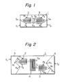
- Fig. 1 which illustrates one conventional acoustic surface wave device
- 1 is a piezoelectric substrate which is made of lithium niobate (LiNb0 3 ) or lithium tantalate (LiTa0 3 ) and is approximately 300 to 500 pm thick.
- An input transducer 2 and an output transducer 3, each of which comprises a pair of separated, interdigitated comb-shaped electrodes, are formed on the plane surface of the substrate 1.
- the transducers 2 and 3 are made of, for example, aluminium which is about 1000 to 5000 A thick.
- the device of Fig. 1 serves as a band-pass filter, a resonator or a delay line.
- S 2 indicates undesired bulk waves which are launched by the input transducer 2 and are propagated through the body of the substrate 1 to reach the output transducer 3;
- S 3 indicates undesired TTEs which are launched by the input transducer 2 and are reflected by the output transducer 3 and, in addition, are reflected by the input transducer 2 to reach the output transducer 3;
- S 4 indicates undesired surface wave reflections and bulks waves which are launched by the input transducer 2 and are reflected by an end face T 1 of the substrate 1 to return to the input transducer 2;
- S 5 indicates undesired surface wave reflections and bulk waves which are launched by the output transducer 3 and are reflected by another end face T 2 of the substrate 1 to return to the output transducer 3. All the waves S 2 , S 3 , S 4 and S 5 deteriorate the band-pass characteristics
- Fig. 2 is a plan view illustrating another conventional acoustic surface wave device.
- an MSC 4 which is composed of a plurality of parallel and equally spaced conductors, and acoustical absorbent layer patterns 5 and 6 are added to Fig. 1.
- the input transducer 2 is located diagonally with respect to the output transducer 3.
- the MSC 4 converts acoustic surface waves from the input transducer 2 into electrical energy and reconverts the electrical energy into other types of acoustic surface waves. That is, the MSC 4 serves as a path changer for the desired acoustic surface waves S 1 , not for the undesired bulk waves 5 2 . Therefore, the bulk waves S 2 do not reach the output transducer 3.
- the TTEs S (not shown in Fig. 2, but in Fig. 1) are suppressed by the MSC 4.
- the acoustical absorbent layer patterns 5 and 6 are formed by coating oleoresion or urearesion by using the screen print method.
- the acoustical absorbent layer patterns 5 and 6 are about 15 to 20 ⁇ m thick.
- the acoustical absorbent layer patterns 5 and 6 have zigzag-shaped or triangular edges facing the input transducer 2 and the output transducer 3.
- the acoustical absorbent layer pattern 5 has a V-shaped recess portion R 1 and a V-shaped protruding portion R 2 .
- the acoustical absorbent layer pattern 5 absorbs most of the undesired waves S 4 from the input transducer 2 and, simultaneously, reflects some of the undesired waves S 4 ; however, in this case, the acoustical absorbent layer pattern 5 changes the direction of the reflections S 4 ' of the waves S 4 , as illustrated in Fig. 3A which is an enlargement of the recess portion R 1 of Fig. 2.
- the acoustical absorbent layer pattern 6 has a V-shaped recess portion R 3 and a V-shaped protruding portion R 4 .
- the acoustical absorbent layer pattern 6 absorbs most of the undesired waves S 5 and, simultaneously, reflects some of the undesired waves S 5 ; however, the direction of the reflections of the undesired waves S 5 is also changed. Therefore, such reflections do not return to the input transducer 2 or to the output transducer 3.
- the acoustical absorbent layer patterns 5 and 6 sometimes spread during the manufacture thereof due to a change of viscosity. Therefore, as illustrated in Fig. 3B, the tip of the V-shaped recess portion R 1 of the acoustical absorbent layer pattern 5 becomes rounded, with the result that it becomes parallel to the wave front of the waves S 4 . As a result, the reflections S 4 ' return to the intput transducer 2, which causes the problem of degration of the band-pass characteristics.
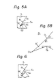
- Fig. 4 is a plan view illustrating one embodiment of the acoustic surface device according to the present invention.
- a further recess portion R l ' (or R 3 ') is provided in the V-shaped recess portion R (or R 3 ).
- the recess portion R 1 ' is formed diagonally with respect to the propagation path of the acoustic surface waves.
- Fig. 5A which is an enlargement of the V-shaped recess portion R 1 of Fig. 4, most of the waves S 4 from the input transducer 2 are absorbed by the acoustical absobent layer pattern 5; however, reflections S 4 ' which correspond to some of the waves S 4 are reflected by the edge 51 of the acoustical absorbent layer pattern 5. Some of the reflections S 4 ' are again reflected by the edge 52 of the acoustical absorbent layer pattern 5. This phenomenon is repeated so that the reflections S 4 ' are attenuated and absorbed.
- Fig. 5B is also an enlargement of the V-shaped recess portion R 1 of Fig. 4. As illustrated in Fig. 5B, for example, the recess portion R 1 ' should be formed so as to satisfy the following conditions: In other words, the position of the tip 0 3 is on the outer side of the tip O 2 . Of course, the position of the tip 0 3 can be on the outer side of the tip O 1 .
- the acoustical absorbent layer patterns 5 and 6 of F ig. 4 can absorb the undesired waves S 4 and S 5 , respectively.
- Fig. 6 is a modification of Fig. 5A.
- the recess portion R 1 ' is V-shaped, while, in Fig. 6, the recess portion R 1 ' is U-shaped. In this case, the same effect can be also expected.
- the inventors compared the attenuation of the reflections to the acoustic surface waves at a frequency of 38.9 MHz.
- the attenuation was -36 dB to -42 dB (average -39 dB)
- the attenuation was -43 dB to -47 dB (average -45 dB).
- an acoustic surface wave device embodying the present invention can be made so that, as compared with the conventional device of Fig. 2, the band-pass characteristics are improved.
Landscapes
- Physics & Mathematics (AREA)
- Acoustics & Sound (AREA)
- Surface Acoustic Wave Elements And Circuit Networks Thereof (AREA)
Applications Claiming Priority (2)
| Application Number | Priority Date | Filing Date | Title |
|---|---|---|---|
| JP12536/81 | 1981-01-30 | ||
| JP56012536A JPS57127321A (en) | 1981-01-30 | 1981-01-30 | Surface acoustic wave filter |
Publications (3)
| Publication Number | Publication Date |
|---|---|
| EP0057598A2 true EP0057598A2 (de) | 1982-08-11 |
| EP0057598A3 EP0057598A3 (en) | 1982-09-08 |
| EP0057598B1 EP0057598B1 (de) | 1985-07-10 |
Family
ID=11808045
Family Applications (1)
| Application Number | Title | Priority Date | Filing Date |
|---|---|---|---|
| EP82300487A Expired EP0057598B1 (de) | 1981-01-30 | 1982-01-29 | Akustische Oberflächenwellenvorrichtung |
Country Status (4)
| Country | Link |
|---|---|
| US (1) | US4426595A (de) |
| EP (1) | EP0057598B1 (de) |
| JP (1) | JPS57127321A (de) |
| DE (1) | DE3264604D1 (de) |
Cited By (1)
| Publication number | Priority date | Publication date | Assignee | Title |
|---|---|---|---|---|
| WO1992017937A1 (de) * | 1991-03-28 | 1992-10-15 | Siemens Aktiengesellschaft | Oberflächenwellenanordnung mit einer struktur zur vermeidung störender akustischer wellenanteile |
Families Citing this family (6)
| Publication number | Priority date | Publication date | Assignee | Title |
|---|---|---|---|---|
| DE3234955A1 (de) * | 1982-09-21 | 1984-03-22 | Siemens AG, 1000 Berlin und 8000 München | Oberflaechenwellenfilter, sowie verfahren zur herstellung des oberflaechenwellenfilters |
| JPS6237441U (de) * | 1985-08-22 | 1987-03-05 | ||
| US4745321A (en) * | 1985-10-24 | 1988-05-17 | Texas Instruments Incorporated | Reflective array surface acoustic wave device |
| US4680497A (en) * | 1986-04-28 | 1987-07-14 | Northern Telecom Limited | Surface acoustic wave devices |
| JP2000181461A (ja) | 1998-12-10 | 2000-06-30 | Kumamoto Nippon Denki Kk | 機械音を発生する機械の吸音装置 |
| JP2004297693A (ja) * | 2003-03-28 | 2004-10-21 | Fujitsu Media Device Kk | 弾性表面波デバイスの製造方法及び弾性表面波デバイス |
Family Cites Families (5)
| Publication number | Priority date | Publication date | Assignee | Title |
|---|---|---|---|---|
| JPS5847089B2 (ja) * | 1976-02-10 | 1983-10-20 | 株式会社東芝 | カラ−テレビジヨン受像機pif表面波フイルタ |
| JPS5333557A (en) | 1976-08-24 | 1978-03-29 | Toshiba Corp | Elastic surface wave element |
| JPS53109458A (en) | 1977-03-07 | 1978-09-25 | Hitachi Ltd | Element for elastic surface wave |
| US4146851A (en) | 1977-06-23 | 1979-03-27 | Gte Laboratories Incorporated | Acoustic surface wave device |
| JPS5693414A (en) | 1979-12-27 | 1981-07-29 | Fujitsu Ltd | Elastic surface wave element |
-
1981
- 1981-01-30 JP JP56012536A patent/JPS57127321A/ja active Pending
-
1982
- 1982-01-22 US US06/341,683 patent/US4426595A/en not_active Expired - Fee Related
- 1982-01-29 DE DE8282300487T patent/DE3264604D1/de not_active Expired
- 1982-01-29 EP EP82300487A patent/EP0057598B1/de not_active Expired
Cited By (2)
| Publication number | Priority date | Publication date | Assignee | Title |
|---|---|---|---|---|
| WO1992017937A1 (de) * | 1991-03-28 | 1992-10-15 | Siemens Aktiengesellschaft | Oberflächenwellenanordnung mit einer struktur zur vermeidung störender akustischer wellenanteile |
| US5414321A (en) * | 1991-03-28 | 1995-05-09 | Siemens Aktiengesellschaft | Surface-wave arrangement having a structure for preventing interfering acoustic wave components |
Also Published As
| Publication number | Publication date |
|---|---|
| EP0057598A3 (en) | 1982-09-08 |
| DE3264604D1 (en) | 1985-08-14 |
| JPS57127321A (en) | 1982-08-07 |
| EP0057598B1 (de) | 1985-07-10 |
| US4426595A (en) | 1984-01-17 |
Similar Documents
| Publication | Publication Date | Title |
|---|---|---|
| US3980904A (en) | Elastic surface wave device | |
| EP0026114A1 (de) | Vorrichtung mit akustischen Oberflächenwellen | |
| EP0057598B1 (de) | Akustische Oberflächenwellenvorrichtung | |
| US4201964A (en) | Elastic surface wave device | |
| JPH0410765B2 (de) | ||
| US4350963A (en) | Surface acoustic wave device | |
| US4814658A (en) | SAW device with continuous finger pattern | |
| US4047130A (en) | Surface acoustic wave filter | |
| EP0044732B1 (de) | Akustischer Oberflächenwellenwandler mit verbesserter Frequenzcharakteristik | |
| EP0197640B2 (de) | Akustische Oberflächenwellenanordnungen mit Fingern zur Unterdrückung von Reflexionen | |
| KR100221230B1 (ko) | 자유단선 반사형 표면 음향파 장치 | |
| CA1129511A (en) | Elastic surface wave device | |
| US4472694A (en) | Acoustic surface wave device | |
| US4205285A (en) | Acoustic surface wave device | |
| JPS6231860B2 (de) | ||
| US4516094A (en) | Acoustic surface wave device | |
| EP0028265B1 (de) | Einrichtung mit akustischen oberflächenwellen | |
| US4410824A (en) | Means for preventing cracks in the gap region of a surface acoustic wave device | |
| US4603275A (en) | Surface acoustic wave device using beveled substrate | |
| US6911881B2 (en) | Surface acoustic wave device | |
| US4101852A (en) | Microacoustic shear bulk wave device | |
| JPH0245364B2 (de) | ||
| JPH0241925B2 (de) | ||
| JPS6345055Y2 (de) | ||
| JPS60263506A (ja) | 弾性表面波帯域通過フイルタ装置 |
Legal Events
| Date | Code | Title | Description |
|---|---|---|---|
| PUAI | Public reference made under article 153(3) epc to a published international application that has entered the european phase |
Free format text: ORIGINAL CODE: 0009012 |
|
| PUAL | Search report despatched |
Free format text: ORIGINAL CODE: 0009013 |
|
| AK | Designated contracting states |
Designated state(s): DE FR GB |
|
| AK | Designated contracting states |
Designated state(s): DE FR GB |
|
| 17P | Request for examination filed |
Effective date: 19821202 |
|
| GRAA | (expected) grant |
Free format text: ORIGINAL CODE: 0009210 |
|
| AK | Designated contracting states |
Designated state(s): DE FR GB |
|
| REF | Corresponds to: |
Ref document number: 3264604 Country of ref document: DE Date of ref document: 19850814 |
|
| ET | Fr: translation filed | ||
| PLBE | No opposition filed within time limit |
Free format text: ORIGINAL CODE: 0009261 |
|
| STAA | Information on the status of an ep patent application or granted ep patent |
Free format text: STATUS: NO OPPOSITION FILED WITHIN TIME LIMIT |
|
| 26N | No opposition filed | ||
| PGFP | Annual fee paid to national office [announced via postgrant information from national office to epo] |
Ref country code: GB Payment date: 19911112 Year of fee payment: 11 |
|
| PGFP | Annual fee paid to national office [announced via postgrant information from national office to epo] |
Ref country code: FR Payment date: 19911227 Year of fee payment: 11 |
|
| PGFP | Annual fee paid to national office [announced via postgrant information from national office to epo] |
Ref country code: DE Payment date: 19920326 Year of fee payment: 11 |
|
| PG25 | Lapsed in a contracting state [announced via postgrant information from national office to epo] |
Ref country code: GB Effective date: 19930129 |
|
| GBPC | Gb: european patent ceased through non-payment of renewal fee |
Effective date: 19930129 |
|
| PG25 | Lapsed in a contracting state [announced via postgrant information from national office to epo] |
Ref country code: FR Effective date: 19930930 |
|
| PG25 | Lapsed in a contracting state [announced via postgrant information from national office to epo] |
Ref country code: DE Effective date: 19931001 |
|
| REG | Reference to a national code |
Ref country code: FR Ref legal event code: ST |