EP0057312B1 - Subroutine control circuitry - Google Patents
Subroutine control circuitry Download PDFInfo
- Publication number
- EP0057312B1 EP0057312B1 EP81304886A EP81304886A EP0057312B1 EP 0057312 B1 EP0057312 B1 EP 0057312B1 EP 81304886 A EP81304886 A EP 81304886A EP 81304886 A EP81304886 A EP 81304886A EP 0057312 B1 EP0057312 B1 EP 0057312B1
- Authority
- EP
- European Patent Office
- Prior art keywords
- subroutine
- address
- stack
- return
- task
- Prior art date
- Legal status (The legal status is an assumption and is not a legal conclusion. Google has not performed a legal analysis and makes no representation as to the accuracy of the status listed.)
- Expired
Links
- 230000015654 memory Effects 0.000 claims description 18
- 230000004044 response Effects 0.000 claims description 18
- 238000012545 processing Methods 0.000 claims description 16
- VLCQZHSMCYCDJL-UHFFFAOYSA-N tribenuron methyl Chemical compound COC(=O)C1=CC=CC=C1S(=O)(=O)NC(=O)N(C)C1=NC(C)=NC(OC)=N1 VLCQZHSMCYCDJL-UHFFFAOYSA-N 0.000 claims 2
- 230000008878 coupling Effects 0.000 claims 1
- 238000010168 coupling process Methods 0.000 claims 1
- 238000005859 coupling reaction Methods 0.000 claims 1
- 230000008021 deposition Effects 0.000 claims 1
- 230000000694 effects Effects 0.000 description 3
- 230000006870 function Effects 0.000 description 2
- 238000010348 incorporation Methods 0.000 description 2
- 238000000034 method Methods 0.000 description 2
- 238000013459 approach Methods 0.000 description 1
- 230000005540 biological transmission Effects 0.000 description 1
- 238000013461 design Methods 0.000 description 1
- 238000011161 development Methods 0.000 description 1
- 230000018109 developmental process Effects 0.000 description 1
- 238000012423 maintenance Methods 0.000 description 1
- 239000002699 waste material Substances 0.000 description 1
Images


Classifications
-
- G—PHYSICS
- G06—COMPUTING; CALCULATING OR COUNTING
- G06F—ELECTRIC DIGITAL DATA PROCESSING
- G06F9/00—Arrangements for program control, e.g. control units
- G06F9/06—Arrangements for program control, e.g. control units using stored programs, i.e. using an internal store of processing equipment to receive or retain programs
- G06F9/44—Arrangements for executing specific programs
- G06F9/448—Execution paradigms, e.g. implementations of programming paradigms
- G06F9/4482—Procedural
- G06F9/4484—Executing subprograms
- G06F9/4486—Formation of subprogram jump address
Definitions
- the present invention relates to a subroutine control circuit as set out in the first portion of claim 1.
- Microprogramming may be broadly viewed as a technique for designing and implementing the control function of a digital computer system as sequences of control signals that are organized on a word basis and stored in a fixed or dynamically changeable control memory.
- Detailed examples of some known approaches to the design of microprogrammed digital computers can be found in U.S. Patent No. 3,886,523, Ferguson et al., issued May 27, 1975, U.S. Patent No. 4,155,120, Keefer and Kim, issued May 15, 1979, U.S. Patent No. 4,181,935, Feeser and Gerhold, issued January 1, 1980 and U.S. Patent No. 4,038,643, Kim, issued July 26,1977; in the book by S. S.
- IBM Technical Disclosure Bulletin, Vol. 22, No. 8B of January 1980, in an article by Kiselak and others, pages 3775 ⁇ 3777 discloses a system for automatically providing return addresses for nested subroutines in a microprogrammed data processing system where the latest entry in a stack of subroutine return addresses is provided in a secondary store for immediate access when returning from a subroutine.
- the disclosed -apparatus requires the return address to be calculated before storage requiring the loss of many machine clock cycles for the calculation.
- the apparatus does not allow for the automatic interleaving of tasks in a multiprogramme environment.
- United States Patent 3,805,247 discloses a multiprogrammable multi-task data processing system. Many independent processors are simultaneously operable to perform microprogramme sequences.
- This United States Patent discloses the use of a stack memory for the storage of micro-instruction return addresses.
- the disclosed apparatus in United States Patent 3,805,247 allocates the stack within a conventional memory space.
- the allocation of space within a conventional memory means that the overall system must waste clock cycles in retrieving addresses from the memory. Such allocation further means that the overall system must keep track of the sequence of presented addresses.
- the present invention seeks to improve over the apparatus disclosed in this patent by arranging that return addresses are stored and retrieved without loss of operating cycles in the system and by further arranging that correct control of the presentation of addresses is provided without time wasting system intervention.
- United States Patent 4,041,462 discloses the use of a stack for storing nested microinstruction subroutine return addresses.
- the stack automatically provides desired data by means of a self-incrementing stack address register.
- the disclosed stack has the disadvantage of being usable only for one processor at a time and further has the disadvantage of requiring to have its address register loadable from the processor. Speed of retrieval from the stack is limited to stack speed.
- the present invention seeks to improve over the apparatus disclosed in United States Patent 4,041,462 by providing a microinstruction subroutine return address store automatically operable in a multiprocessor multi-task environment requiring no intervention on the part of any processor for its automatic maintenance.
- United States Patent 4,156,925 discloses a data processing system having plural phase clocks for operating a plurality of processors, each employing its own set of microinstructions.
- United States Patent 4,156,925 discloses the simultaneous interleaved operation of three sets of micro- instructions where each set has its own independently addressable store on its respective clock cycle.
- Each microinstruction contains information for the address of the next micro- instruction in each sequence.
- the disclosed microinstruction memories store each micro- instruction in a sequence. The disclosed memory stores further require to be provided with separate clock signals.
- the present invention seeks to improve over the system disclosed in United States Patent, 4,156,925 by providing a system storing only subroutine return addresses, and automatically operable without system intervention to present a correct return address without the necessity for generating separate clock signals for each programme sequence.
- the matter disclosed in United States Patent 4,156,925 is of the type wherein the present invention may be advantageously applied.
- the present invention may be used to provide subroutine return addresses for use in addressing the micro- instruction stores disclosed in United States Patent 4,156,925.
- An object of the invention is to provide multi-phase subroutine control circuitry in a data processing system which can accommodate many levels of subroutine entry and which provides for sharing subroutines among a large plurality of instructions and/or tasks.
- the present invention consists in a subroutine control circuit for the receipt, storage and ordered retrieval of a sequence of subroutine return addresses for a corresponding linked and nested sequence of subroutines in a data processing system utilizing a microprogramme sequence of independently addressable microinstructions, said circuit including a stack store and a fast access file both coupled to receive an input return address from said system, operable to store said input return address in response to the receipt from said system of subroutine entry indication, and operable in response to the receipt from said system of a subroutine return indication to provide as output the next previously stored unretrieved return address, the fast access file (52) being operable in response to the receipt from said system of a subroutine return indication to deliver up to said system the return address stored therein and operable thereafter to receive and store said output of said stack and indicator logic coupled to receive and monitor said subroutine entry indications and said subroutine return indications and operable to provide to said system indication when said stack is empty or overflowing, said circuit being characterised by being coupled to receive
- the invention is adapted for incorporation in a data processing system of the type disclosed in the aforementioned patent applications wherein a plurality of tasks are concurrently performed in a manner so as to provide for the multiprogramming and multiprocessing of tasks at a microinstruction level.
- a particularly advantageous subroutine control capability is provided using a plurality of selectably accessible stacks, one for each task, along with corresponding pointer registers.
- a relatively faster access register is provided for storing the most recent return address of each task so as to permit return addresses to be rapidly made available when required.
- Operation is provided in a manner which permits multiple levels of subroutine entry to be accommodated for each task, while also permitting many tasks to share the same subroutines.
- subroutine control operations are staged for performance in a multiprogramming and multiprocessing environment so as to be able to provide multi-phase subroutine control for a plurality of concurrently executing tasks.
- high level input instructions are viewed as a plurality of tasks to be performed.
- Each task is divided into one or more task microinstructions.
- Execution of each task microinstruction is performed over three stages (Read, Compute and Write), each stage requiring one clock.
- Multiprogramming is achieved by providing for the performance of task microinstructions in an intermixed fashion regardless of the task to which each task micro- instruction belongs.
- Multiprocessing is achieved by employing a threestage pipelined architecture in a manner which in effect performs as three separate processors operating 120° out of phase with one another and sharing the same physical hardware.
- each processor executes a different one of the Read, Compute and Write stages corresponding to a different task microinstruction.
- a Read operation is capable of being performed for a first task micro- instruction
- a Compute operation is capable of being performed for a second task micro- instruction
- a Write operation is capable of being performed for a third task microinstruction.
- Figs. 1 and 2 illustrate examples of the operation of the system disclosed in the aforementioned patent applications.
- Fig. 1 basically illustrates how three 120° out-of-phase processors provide for the concurrent performance of the three task microinstructions Txm, Tym, and T z m.
- the letters R, C and W in Fig. 1 respectively designate the three successive Read, Write and Compute stages performed in executing each task microinstruction.
- Typical 3-stage operation of a task microinstruction in the system of the aforementioned applications is as follows.
- a Read operation is performed to prepare for execution of a particular selected task microinstruction. This includes reading out from storage the appropriate operand data to be used during microinstruction execution, reading out condition select data for use in determining the next microinstruction address, and decoding appropriate fields of the micro- instruction to derive control signals for use in controlling data path functions during the next following Compute stage.
- a Compute operation is performed during which the selected microinstruction is executed. Also, selected conditions (determined by the condition select data read out during the Read stage) are used to produce next microinstruction data.
- next following Write stage which is the last stage in the execution of a task micro- instruction
- a Write operation is performed during which the results of microinstruction execution are written into storage.
- the next micro- instruction data produced during the Compute stage is used to select the next microinstruction.
- Fig. 2 is an example of how the system disclosed in the aforementioned patent applications provides for the execution of task micro- instructions in a manner which takes advantage of both multiprogramming and multiprocessing.
- the ten tasks T A through T j are characterized as follows:
- next microinstruction data indicates that the next task microinstruction to be executed for this task is the first task microinstruction of a subroutine.
- the next microinstruction data not only provides the address of the first microinstruction of the subroutine, but also provides a subroutine entry signal E along with a signed offset value F.
- This signed offset value F has a value such that the return microinstruction address for the subroutine is obtainable by adding this signed offset value F to the address of the present micro- instruction PA.
- the system provides a return signal R requesting that the appropriate return address be provided for use as the next microinstruction address.
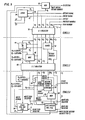
- Fig. 3 illustrates a preferred implementation of multi-level subroutine control circuitry adapted for use in the system of the aforementioned patent applications.
- the entry signal E provided by the system when a subroutine is to be entered causes the subroutine control circuitry of Fig. 3 to add the signed offset value F to the present microinstruction address PA to form the return address RA.
- This calculated return address RA is then stored in a stack corresponding to the task which produced the entry signal E (there being one such stack for each task), and the stack level pointer is incremented by one and saved in a respective register.
- each stack may accommodate, for example, fifteen levels of subroutine entry so that as many as fifteen return addresses can be stored in the corresponding stack for each task.
- a subroutine return is initiated when the system provides a return signal R during a Compute stage of task execution. This return signal causes the separately stored most recent return address for the task to be sent to the system and to be replaced in this separate storage by the next most recent return address for that task.
- the corresponding stack pointer for the task is decremented by one to reflect that this most recent return address has been sent to the system.
- the above summarized subroutine control operations of the preferred implementation illustrated in Fig. 3 are performed in three stages which operate in synchronism with the previously described three-stage Read, Compute and Write operations of the system disclosed in the aforementioned patent applications so as to be able to take advantage of, as well as contribute to, the multiprogramming and multiprocessing capabilities of this system as illustrated in Figs. 1 and 2. More specifically, the preferred subroutine control circuitry illustrated in Fig. 3 is constructed and arranged in a manner so as to in effect provide three separate subroutine control circuits operating 120° out of phase with one another with each circuit providing subroutine control for a different task.
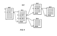
- Fig. 4 illustrates a task T which, for example, includes four subroutine calls SUB-1, SUB-2, SUB-3 and SUB-4.
- Fig. 5 illustrates the contents of the return address stack 20 and fast access register 22 for task T at particular time periods to-t 8 during performance of the task.
- task T comprises a main portion and three subroutine calls SUB-1, SUB-2, SUB-3 and SUB-4.
- the stack 20 and the fast access return address register 22 are empty, and the stack pointer P points to level 0.
- the stack pointer P is decremented by 1 to point to level 1 so as to indicate that level 1 is the next available stack location.
- RTN-2 As illustrated in Fig. 4, during the performance of SUB-1, SUB-2 is encountered at time t 2 . As indicated for t 2 in Fig. 5, the return address RTN-2 for SUB-2 is calculated and stored at level 2 in stack 20 and the pointer P is incremented by 1 to point to level 2. RTN-2 also replaces RTN-1 in the fast access register 22, since RTN-2 is now the most recent return address.
- a third subroutine SUB-3 is encountered at time t 3 which now causes a third return address RTN-3 to be calculated and placed in level 2 of stack 20 and also in the fast access register 22, as shown for t 3 in Fig. 5. Also, the pointer P is incremented by 1 to now point to level 3.
- SUB-3 is completed at time t 4 (Fig. 4)
- the corresponding return address RTN-3 is rapidly accessed from the fast access register 22 and is replaced by the next most recent return address RTN-2 from the stack 20, as indicated for time t 4 in Fig. 5.
- pointer P is decremented by one to point to level 2.
- SUB-4 is encountered (Fig. 4) which, as shown fort 6 in Fig. 5, causes the corresponding calculated return address RTN-4 to be placed in stack 20 at level 1 and also to be placed in the fast access register 22; the pointer P is incremented to point to level 2.
- SUB-4 is completed at t 7 (Fig. 4)
- the return address RTN-4 is accessed from the fast access register 22 and is replaced by the next most recent return address RTN-1, as shown for t 7 in Fig. 5, while the pointer P is decremented by 1 to point to level 1.
- SUB-1 then continues and is completed at t 8 , at which time RTN-1 is accessed from the fast access register 22 and processing returns to the main portion of task T. Accordingly, as illustrated for t 8 in Fig. 5, stack 20 and the fast access register 22 are now empty and the pointer P is pointing to level 0.
- the subroutine control operations provided by the preferred implementation illustrated in Fig. 3 are staged in a manner so as to in effect provide three separate subroutine control circuits operating 120° out of phase with one another with each circuit providing subroutine control for a different task. Accordingly, it is to be understood that, in the preferred implentations of Fig. 3, the operations for the illustrative task T described above in conjunction with Figs. 4 and 5 may be performed concurrently, but 120° out of phase with one another, for up to three different tasks.
- subroutine control stages S-1, S-2 and S-3 perform their respective operations in synchronism with the Compute, Write and Read stages, respectively, of the system of the aforementioned patent applications which system was briefly described in connection with Figs. 1 and 2.
- Fig. 6 is a generally similar type of illustration as Fig. 1 with the additional showing of the corresponding subroutine control stages S-1, S-3 and S-3 occurring during particular illustrative examples of subroutine entry and return for each task.
- Fig. 6 similar to Fig. 1, illustrates the concurrent performance of tasks T x , Ty and T z by processors #1, #2 and #3, respectively, operating 120° out of phase with one another.
- the first illustrated task microinstructions T x m, Tym, and T z m, of tasks T x , Ty and T z , respectively, in Fig. 6, each provide a subroutine entry signal during its Compute (C) operation indicating that the next task microinstruction for the respective task (T x S 1, Tys, or T z S 1 ) is to be the first microinstruction of a particular subroutine.
- C Compute
- subroutine operations comprised of stages S-1, S-2 and S-3 are again initiated in response to a subroutine return signal R provided by the system during the corresponding Compute operation, causing the corresponding return address in the respective fast access register 22 to be transmitted to the system for use as the next microinstruction address for its respective task, while also causing the corresponding stack level pointer P to be decremented and the next most recent return address (if present) to be stored in the fast access register 22 (note, for example, time period t 4 in Figs. 4 and 5).
- subroutine entry and return operations shown for exemplary purposes in Fig. 6 may occur independently for each processor and need not occur at the particular times indicated.
- the particular times illustrated in Fig. 6 are instructive, however, in demonstrating how subroutine control operations may typically be performed concurrently for up to three tasks in the preferred implementations being described herein, and also in synchronism with corresponding Compute, Write and Read operations of the system.
- each stage is performed during one clock period, and that during a single clock period, each stage may be performing its operations for a different task.
- note clock period 4 in Fig. 6 during which an S-1 operation is performed for task T x , an S-2 operation is performed for task Ty, and an S-3 operation is performed for task T z .
- stage S-1 includes an S-1 register 30, a multiplexer 32, and logic 34.
- the S-1 register 30 serves to store the subroutine signals provided during the compute operation of a task microinstruction when either a subroutine entry or subroutine return situation is indicated. If a subroutine entry is indicated, the subroutine signals designate the following: a task number T 1 (which is also applied to stage S-3), a present address PA,, a signed offset value F 1 , the next available stack level indicated by pointer P, (which is provided by stage S-3 in response to T 1 ), and a subroutine entry signal E 1 .
- the subroutine signals provided designate just the task number T 1 , the next available stack level indicated by pointer P 1 (provided by stage S-3), and a subroutine return R 1 .
- the task number T 1 applied to stage S-3 causes the most recent return address for the task to be applied to the input of the multiplexer 32; the return signal R 1 applied to the multiplexer 32 during S-1 of a subroutine return then causes this return address to be transmitted to the system for the use as the next microinstruction address for this task.
- Stage S-1 also includes logic 34 to which E 1 , R 1 and P 1 are applied.
- E 1 logic 34 determines if the respective stack level pointer P 1 is at its highest level; if so, an overflow signal OV is produced indicating that the respective stack for task T 1 is full and cannot accept another return address.
- R 1 logic 34 determines if the respective stack level pointer P 1 is at its lowest level; if so, a signal EO is produced indicating that the respective stack for T 1 is empty. The system may then take appropriate action in response to an OV or EO signal.
- Stage S-2 includes an S-2 register 40, an adder 42, an incrementer/decrementer 46 and a multiplexer 44. It will be noted in Fig. 3 that the subscripts of the signals provided to stage S-2 are changed from “2" to "1". This is done to indicate that these signals which were applied to stage S-1 during the previous clock period are now being applied to stage S-2 in the next clock period. These "2" subscripts also serve to distinguish these signals applied to S-2 from the new set of subscript "1" signals which are concurrently applied during the same clock period to stage S-1 for a different task, as previously explained in connection with Fig. 6 (see, for example, clock period 3 in Fig. 6). A similar convention is used in connection with signals applied to S-3.
- the return address RA 2 for the respective task is calculated by the adder 42 by adding the present address PA 2 to the offset value F 2 .
- This calculated return address RA 2 is then stored in the S-2 register 40 along with the respective task number T 2 and the entry signal E 2 .
- the entry signal E 2 produced for subroutine entry causes the incrementer/decrementer 44 to increment the pointer P 2 by one and also causes the multiplexer 46 to output the unchanged P 2 value, these values of P 2 and P 2 +1 also being stored in the S-2 register 40.
- stage S-2 of a subroutine return only P 2 , R 2 and T 2 are present. Operation during S-2 is then such that R 2 causes the incrementer/decrementer 44 to decrement P 2 by one and to also cause the multiplexer 46 to pass the resulting P 2 -1 value for storage in respective locations in the S-2 register 40 along with R 3 and T 2 .
- stage S-3 includes a return address stack storage 50, a fast access register file 52, a stack pointer register file 54, an OR gate 56 and a multiplexer 58.
- the return address stack storage 50 comprises a random access memory which provides storage for a plurality of stacks, one for each task. A single one of these stacks is illustrated by the stack 20 in Fig. 5.
- the fast access register file 52 provides rapidly accessible storage for a plurality of fast access registers, a single one of these registers being illustrated by the register 22 in Fig. 5.
- the stack pointer register file 54 provides storage for a plurality of stack level pointer registers, also one for each task.
- the return address stack storage 50 is capable of being enabled during each clock period either for writing (for a subroutine entry) or for reading (for a subroutine return). Accordingly, E 3 serves as a write enable for storage 50 and R 3 serves as a read enable
- the fast access register file 52 and the stack pointer register file 54 are capable of providing both writing and reading from different registers during each clock period. This capability is provided for files 52 and 54 in order to permit all three of the subroutine stages S-1, S-2, and S-3 to be performed during each clock period for different tasks as illustrated, for example, in Fig. 6. Reading is always provided during a clock period, while writing is enabled by either E 3 or R 3 . This is implemented in Fig.
- T 3 serves as a stack selector for the return address stack storage 50, and as a write register selector for both the fast access register file 52 and the stack pointer register file 54.
- T 1 serves as a read select register for both files 52 and 54.
- the level pointer for the return address stack storage is P 3 for a subroutine entry or P a -1 for a subroutine return.
- E 3 provides a write enable for the return address storage 50 so as to cause the return address RA 3 (calculated during S-2) to be written into the particular stack selected by task T 3 at the level pointed to by pointer P 3 .
- This return address is also written, via multiplexer 58, into the particular fast access register in file 52 selected by T 3 (see, for example, Fig. 5, time t i ).
- the operation of the multiplexer 58 is such that, during a subroutine entry (when R 3 is absent), the multiplexer 58 passes RA 3 rather than the output of the return address stack storage 50.
- the incremented level pointer P 3 +1 is written into the particular stack pointer register in file 54 selected by T 3 .
- stage S-3 of a subroutine return operations differ from those performed for a subroutine entry primarily in that there is no return address to be written in the return address stack storage 50. Instead, the storage 50 is enabled for reading by R 3 .
- T 3 still selects the stack in storage 50 and the register in file 52 which are to be accessed, but the stack level pointer will now have a value of P 3 -1 (as a result of being decremented by one during S-2) so as to read out the next most recent return address for task T 3 which passes, via the multiplexer 58, to the fast access register file 52 for writing in the corresponding fast access register of T 3 (see Fig. 6, e.g., time t 2 ).
- stage S-3 of a subroutine return the decremented level pointer P 3 -1 is written into the stack pointer register of file 54 selected by T 3 in order to adjust the level pointer value to account for the reading out from storage 50 of the next most recent return address.
- stage S-3 concurrently with the writing during stage S-3 of a return address in the particular fast access register of file 52 selected by T 3 , the task number T 1 applied to stage S-1 during the same clock period is also applied to file 52 of stage S-3 to select a corresponding fast access register for reading out the most recent return address forT1.
- this accessed return address is applied to the multiplexer 32 of stage S-1 for transmission to the system in the event that a subroutine return is indicated for stage S-1.
- stage S-3 concurrently with the writing during stage S-3 of a level pointer value in the particular register in the stack pointer register file 54 selected by T 3 , the task number T 1 applied to stage S-1 during the same clock period is also applied to file 54 of stage S-3 to select a corresponding stack pointer register for reading out the current value of the level pointer for task T 1 for use as the P 1 value for the concurrently performed stage S-1 operations.
Landscapes
- Engineering & Computer Science (AREA)
- Software Systems (AREA)
- Theoretical Computer Science (AREA)
- Physics & Mathematics (AREA)
- General Engineering & Computer Science (AREA)
- General Physics & Mathematics (AREA)
- Executing Machine-Instructions (AREA)
Description
- The present invention relates to a subroutine control circuit as set out in the first portion of
claim 1. - Microprogramming may be broadly viewed as a technique for designing and implementing the control function of a digital computer system as sequences of control signals that are organized on a word basis and stored in a fixed or dynamically changeable control memory. Detailed examples of some known approaches to the design of microprogrammed digital computers can be found in U.S. Patent No. 3,886,523, Ferguson et al., issued May 27, 1975, U.S. Patent No. 4,155,120, Keefer and Kim, issued May 15, 1979, U.S. Patent No. 4,181,935, Feeser and Gerhold, issued January 1, 1980 and U.S. Patent No. 4,038,643, Kim, issued July 26,1977; in the book by S. S. Husson, "Microprogramming; Principles and Practices", Prentice-Hall, Inc. (1970); in the book "Foundations of Microprogramming", Argrausaia, et al., Academic Press, Inc., 1976; in the article "Microprogramming-Another Look at Internal Computer Control", M. J. Flynn, I.E.E.E. Proc., Vol. 63, No. 11, Nov. 1975, pp. 1554-1567; and in the article "Microprogramming: a Tutorial and Survey of Recent Developments", I.E.E.E. Transactions on Computers, Vol. C-29, No. 1, Jan. 1980.
- In recent years the concept of microprogramming has been extended for use in conjunction with pipelined architectures as described, for example, in the article "The Microprogramming of Pipelined Processors", P. M. Kogge, 4th Annual Symposium on Computer Architecture, Mar. 1977, pp. 63-69; and also the article "A Pipeline Architecture Oriented Towards Efficient Multitasking", F. Romani, Euromicro, Oct. 1976, Vol. 2, No. 4, North-Holland Publishing Co., Amsterdam.
- In the copending European patent applications EP-A-57313 (published 11.8.82) and EP-A-59810 (published 15.9.82), referred herein as aforementioned patent applications an embodiment of a microprogrammed data processing system is disclosed which provides for the execution of tasks in a manner so as to achieve the advantages of both multiprogramming and microprocessing of tasks at a micro-instruction level. One object of the present invention is to provide improved means and methods for controlling subroutine operations in a system of this type.
- IBM Technical Disclosure Bulletin, Vol. 22, No. 8B of January 1980, in an article by Kiselak and others, pages 3775―3777 discloses a system for automatically providing return addresses for nested subroutines in a microprogrammed data processing system where the latest entry in a stack of subroutine return addresses is provided in a secondary store for immediate access when returning from a subroutine. The disclosed -apparatus requires the return address to be calculated before storage requiring the loss of many machine clock cycles for the calculation. The apparatus does not allow for the automatic interleaving of tasks in a multiprogramme environment.
- United States Patent 3,805,247, discloses a multiprogrammable multi-task data processing system. Many independent processors are simultaneously operable to perform microprogramme sequences. This United States Patent discloses the use of a stack memory for the storage of micro-instruction return addresses. The disclosed apparatus in United States Patent 3,805,247 allocates the stack within a conventional memory space. The allocation of space within a conventional memory means that the overall system must waste clock cycles in retrieving addresses from the memory. Such allocation further means that the overall system must keep track of the sequence of presented addresses. The present invention seeks to improve over the apparatus disclosed in this patent by arranging that return addresses are stored and retrieved without loss of operating cycles in the system and by further arranging that correct control of the presentation of addresses is provided without time wasting system intervention.
- United States Patent 4,041,462 discloses the use of a stack for storing nested microinstruction subroutine return addresses. The stack automatically provides desired data by means of a self-incrementing stack address register. The disclosed stack has the disadvantage of being usable only for one processor at a time and further has the disadvantage of requiring to have its address register loadable from the processor. Speed of retrieval from the stack is limited to stack speed. The present invention seeks to improve over the apparatus disclosed in United States Patent 4,041,462 by providing a microinstruction subroutine return address store automatically operable in a multiprocessor multi-task environment requiring no intervention on the part of any processor for its automatic maintenance.
- United States Patent 4,156,925, discloses a data processing system having plural phase clocks for operating a plurality of processors, each employing its own set of microinstructions. United States Patent 4,156,925 discloses the simultaneous interleaved operation of three sets of micro- instructions where each set has its own independently addressable store on its respective clock cycle. Each microinstruction contains information for the address of the next micro- instruction in each sequence. The disclosed microinstruction memories store each micro- instruction in a sequence. The disclosed memory stores further require to be provided with separate clock signals. The present invention seeks to improve over the system disclosed in United States Patent, 4,156,925 by providing a system storing only subroutine return addresses, and automatically operable without system intervention to present a correct return address without the necessity for generating separate clock signals for each programme sequence. The matter disclosed in United States Patent 4,156,925 is of the type wherein the present invention may be advantageously applied. The present invention may be used to provide subroutine return addresses for use in addressing the micro- instruction stores disclosed in United States Patent 4,156,925.
- In an article in the magazine "Computer", May 1977 on
pages - An object of the invention is to provide multi-phase subroutine control circuitry in a data processing system which can accommodate many levels of subroutine entry and which provides for sharing subroutines among a large plurality of instructions and/or tasks.
- The present invention consists in a subroutine control circuit for the receipt, storage and ordered retrieval of a sequence of subroutine return addresses for a corresponding linked and nested sequence of subroutines in a data processing system utilizing a microprogramme sequence of independently addressable microinstructions, said circuit including a stack store and a fast access file both coupled to receive an input return address from said system, operable to store said input return address in response to the receipt from said system of subroutine entry indication, and operable in response to the receipt from said system of a subroutine return indication to provide as output the next previously stored unretrieved return address, the fast access file (52) being operable in response to the receipt from said system of a subroutine return indication to deliver up to said system the return address stored therein and operable thereafter to receive and store said output of said stack and indicator logic coupled to receive and monitor said subroutine entry indications and said subroutine return indications and operable to provide to said system indication when said stack is empty or overflowing, said circuit being characterised by being coupled to receive from said system a task indication indicative of to which one out of a possible plurality of independent nested subroutine tasks a return address refers on receipt of said entry indication and otherwise indicative of to which one out of said plurality of tasks a return indication refers, by said stack store comprising a separate stack memory for each one of said possible plurality of tasks, by said fast access file, comprising a separate fast access memory for each of said possible plurality of tasks, by said task indication being coupled as an addressing input to said stack and to said fast access file to select respectively the stack memory and the fast access memory appropriate to said indicated task for the storage of a return address and by said fast access file being coupled to receive said task indication for the selection of the contents of the appropriate fast access memory to said task indication for said delivering up to said system, whereby each out of said plurality of possible tasks is automatically provided with its appropriate subroutine return address.
- In a particular preferred embodiment, the invention is adapted for incorporation in a data processing system of the type disclosed in the aforementioned patent applications wherein a plurality of tasks are concurrently performed in a manner so as to provide for the multiprogramming and multiprocessing of tasks at a microinstruction level. In the preferred embodiment of the present invention, a particularly advantageous subroutine control capability is provided using a plurality of selectably accessible stacks, one for each task, along with corresponding pointer registers. Also, a relatively faster access register is provided for storing the most recent return address of each task so as to permit return addresses to be rapidly made available when required. Operation is provided in a manner which permits multiple levels of subroutine entry to be accommodated for each task, while also permitting many tasks to share the same subroutines. In addition, subroutine control operations are staged for performance in a multiprogramming and multiprocessing environment so as to be able to provide multi-phase subroutine control for a plurality of concurrently executing tasks.
- One way of carrying out the invention is described in detail below with reference to the drawings which illustrate only one specific embodiment.
-
- Figs. 1 and 2 illustrate examples of the operation of the system disclosed in the aforementioned patent applications.
- Fig. 3 is a preferred implementation of multi-level subroutine control circuitry in accordance with the invention.
- Fig. 4 illustrates an example of a typical task listing containing a plurality of subroutine calls.
- Fig. 5 illustrates basic operations of the Fig. 3 implentation during performance of the task of Fig. 4.
- Fig. 6 illustrates time relationships between the performance of the stages of the subroutine control circuitry of Fig. 3 and the stages of the processor system.
- Like numerals and characters represent like elements throughout the figures of the drawings.
- For the purposes of this description, a preferred embodiment of the subroutine control circuitry of the present invention will be described for an implementation which is specifically adapted for incorporation in a data processing system of the type disclosed in the aforementioned patent applications. However, it is to be understood that the subroutine control capability provided by the present invention can also be implemented for use in other types of systems.
- In order to better understand the detailed description of the preferred embodiment of the subroutine control circuitry to be presented herein, a brief description of pertinent portions of the system disclosed in the aforementioned patent applications will first be provided.
- In the preferred embodiment of the data processing system disclosed in the aforementioned patent applications, high level input instructions are viewed as a plurality of tasks to be performed. Each task is divided into one or more task microinstructions. Execution of each task microinstruction is performed over three stages (Read, Compute and Write), each stage requiring one clock. Multiprogramming is achieved by providing for the performance of task microinstructions in an intermixed fashion regardless of the task to which each task micro- instruction belongs. Multiprocessing is achieved by employing a threestage pipelined architecture in a manner which in effect performs as three separate processors operating 120° out of phase with one another and sharing the same physical hardware. During each clock period, each processor executes a different one of the Read, Compute and Write stages corresponding to a different task microinstruction. In other words, during each clock period a Read operation is capable of being performed for a first task micro- instruction, a Compute operation is capable of being performed for a second task micro- instruction, and a Write operation is capable of being performed for a third task microinstruction.
- Figs. 1 and 2 illustrate examples of the operation of the system disclosed in the aforementioned patent applications. Fig. 1 basically illustrates how three 120° out-of-phase processors provide for the concurrent performance of the three task microinstructions Txm, Tym, and Tzm. The letters R, C and W in Fig. 1 respectively designate the three successive Read, Write and Compute stages performed in executing each task microinstruction. Typical 3-stage operation of a task microinstruction in the system of the aforementioned applications is as follows.
- During the first stage, a Read operation is performed to prepare for execution of a particular selected task microinstruction. This includes reading out from storage the appropriate operand data to be used during microinstruction execution, reading out condition select data for use in determining the next microinstruction address, and decoding appropriate fields of the micro- instruction to derive control signals for use in controlling data path functions during the next following Compute stage.
- In this next following Compute stage, a Compute operation is performed during which the selected microinstruction is executed. Also, selected conditions (determined by the condition select data read out during the Read stage) are used to produce next microinstruction data.
- In the next following Write stage, which is the last stage in the execution of a task micro- instruction, a Write operation is performed during which the results of microinstruction execution are written into storage. Also, the next micro- instruction data produced during the Compute stage is used to select the next microinstruction.
- Fig. 2 is an example of how the system disclosed in the aforementioned patent applications provides for the execution of task micro- instructions in a manner which takes advantage of both multiprogramming and multiprocessing. This example in Fig. 2 illustrates the concurrent performance of three calculations (A+B)+(C+D)=H; (A+B)-E=I; and (C+D)-E=J. The ten tasks TA through Tj are characterized as follows:

- It is assumed for the above example that the "operand fetch" tasks TA-TE each require two task microinstructions with at least a three clock wait period (indicated by "w" above) therebetween. It is also assumed that each of the "ADD" and "SUBTRACT" tasks TF- TJ require only one clock period (indicated above and in Fig. 2 by "m" having no subscript). Also note in Fig. 2 that a "No-Op" microinstruction is indicated when no task microinstruction is performed.
- It will be remembered from the above brief description of the preferred embodiment of the data processing system disclosed in the aforementioned applications that, during a Compute operation, a particular task microinstruction is executed and also next microinstruction data is produced. The preferred embodiment of the present invention is concerned with the situation where this next microinstruction data indicates that the next task microinstruction to be executed for this task is the first task microinstruction of a subroutine. When such is the case, the next microinstruction data not only provides the address of the first microinstruction of the subroutine, but also provides a subroutine entry signal E along with a signed offset value F. This signed offset value F has a value such that the return microinstruction address for the subroutine is obtainable by adding this signed offset value F to the address of the present micro- instruction PA. During the Compute stage of the last microinstruction of a subroutine, the system provides a return signal R requesting that the appropriate return address be provided for use as the next microinstruction address.
- Fig. 3 illustrates a preferred implementation of multi-level subroutine control circuitry adapted for use in the system of the aforementioned patent applications. Before describing this implementation in detail, a functional description of its overall operation will first be presented in order to permit the detailed description to be more easily understood.
- The entry signal E provided by the system when a subroutine is to be entered causes the subroutine control circuitry of Fig. 3 to add the signed offset value F to the present microinstruction address PA to form the return address RA. This calculated return address RA is then stored in a stack corresponding to the task which produced the entry signal E (there being one such stack for each task), and the stack level pointer is incremented by one and saved in a respective register. Typically, each stack may accommodate, for example, fifteen levels of subroutine entry so that as many as fifteen return addresses can be stored in the corresponding stack for each task.
- Provision is also made for the most recent return address in each stack to be separately stored in a corresponding fast access register so that it can be rapidly provided to the system for use as a next microinstruction address when a subroutine return is required. It will be remembered that a subroutine return is initiated when the system provides a return signal R during a Compute stage of task execution. This return signal causes the separately stored most recent return address for the task to be sent to the system and to be replaced in this separate storage by the next most recent return address for that task. Also, the corresponding stack pointer for the task is decremented by one to reflect that this most recent return address has been sent to the system.
- The above summarized subroutine control operations of the preferred implementation illustrated in Fig. 3 are performed in three stages which operate in synchronism with the previously described three-stage Read, Compute and Write operations of the system disclosed in the aforementioned patent applications so as to be able to take advantage of, as well as contribute to, the multiprogramming and multiprocessing capabilities of this system as illustrated in Figs. 1 and 2. More specifically, the preferred subroutine control circuitry illustrated in Fig. 3 is constructed and arranged in a manner so as to in effect provide three separate subroutine control circuits operating 120° out of phase with one another with each circuit providing subroutine control for a different task.
- Reference is now directed to the example of Figs. 4 and 5. Fig. 4 illustrates a task T which, for example, includes four subroutine calls SUB-1, SUB-2, SUB-3 and SUB-4. Fig. 5 illustrates the contents of the
return address stack 20 and fast access register 22 for task T at particular time periods to-t8 during performance of the task. - As indicated in Fig. 4, task T comprises a main portion and three subroutine calls SUB-1, SUB-2, SUB-3 and SUB-4. At the beginning of task T (time to), the
stack 20 and the fast accessreturn address register 22 are empty, and the stack pointer P points tolevel 0. When SUB-1 is encountered at time t1, the corresponding return address RTN-1 for SUB-1 is calculated and stored in thestack 20 and also in the fast access register 22 (Fig. 5). The stack pointer P is decremented by 1 to point tolevel 1 so as to indicate thatlevel 1 is the next available stack location. - As illustrated in Fig. 4, during the performance of SUB-1, SUB-2 is encountered at time t2. As indicated for t2 in Fig. 5, the return address RTN-2 for SUB-2 is calculated and stored at
level 2 instack 20 and the pointer P is incremented by 1 to point tolevel 2. RTN-2 also replaces RTN-1 in thefast access register 22, since RTN-2 is now the most recent return address. - During the performance of SUB-2, a third subroutine SUB-3 is encountered at time t3 which now causes a third return address RTN-3 to be calculated and placed in
level 2 ofstack 20 and also in thefast access register 22, as shown for t3 in Fig. 5. Also, the pointer P is incremented by 1 to now point tolevel 3. When SUB-3 is completed at time t4 (Fig. 4), the corresponding return address RTN-3 is rapidly accessed from thefast access register 22 and is replaced by the next most recent return address RTN-2 from thestack 20, as indicated for time t4 in Fig. 5. Also note for t4 in Fig. 5 that, since a return is performed, pointer P is decremented by one to point tolevel 2. It will be understood that the return address RTN-3 may still reside inlevel 2, but this is of no significance since it will be written over iflevel 2 receives another return address. Accordingly, for clarity,level 2 is shown empty for t4 in Fig. 5. This convention is used throughout Fig. 5. - As illustrated in Fig. 4, after completion of SUB-3 at t4, SUB-2 continues and is completed at ts. The corresponding return address RTN-2 in the
fast access register 22 is thus accessed and replaced by the next most recent address RTN-1, and the pointer P is decremented by 1 to point tolevel 1, as indicated at tr, in Fig. 5. - At time t6, SUB-4 is encountered (Fig. 4) which, as shown fort6 in Fig. 5, causes the corresponding calculated return address RTN-4 to be placed in
stack 20 atlevel 1 and also to be placed in thefast access register 22; the pointer P is incremented to point tolevel 2. When SUB-4 is completed at t7 (Fig. 4), the return address RTN-4 is accessed from thefast access register 22 and is replaced by the next most recent return address RTN-1, as shown for t7 in Fig. 5, while the pointer P is decremented by 1 to point tolevel 1. - As shown in Fig. 4, SUB-1 then continues and is completed at t8, at which time RTN-1 is accessed from the
fast access register 22 and processing returns to the main portion of task T. Accordingly, as illustrated for t8 in Fig. 5, stack 20 and the fast access register 22 are now empty and the pointer P is pointing tolevel 0. - As pointed out earlier herein, the subroutine control operations provided by the preferred implementation illustrated in Fig. 3 are staged in a manner so as to in effect provide three separate subroutine control circuits operating 120° out of phase with one another with each circuit providing subroutine control for a different task. Accordingly, it is to be understood that, in the preferred implentations of Fig. 3, the operations for the illustrative task T described above in conjunction with Figs. 4 and 5 may be performed concurrently, but 120° out of phase with one another, for up to three different tasks. This is accomplished by providing three successive stages S-1, S-2 and S-3 (one clock per stage) for the performance of the subroutine control operations required in response to a subroutine entry or in response to a subroutine return for a particular task. In addition, provision is made to perform all three stages S-1, S-2 and S-3 during a single clock period in a manner so that, during each clock period, each of stages S-1, S-3 and S-3 performs its respective subroutine operations for a different task.
- It is also to be noted that these subroutine control stages S-1, S-2 and S-3 perform their respective operations in synchronism with the Compute, Write and Read stages, respectively, of the system of the aforementioned patent applications which system was briefly described in connection with Figs. 1 and 2. Such operation is illustrated in Fig. 6 which is a generally similar type of illustration as Fig. 1 with the additional showing of the corresponding subroutine control stages S-1, S-3 and S-3 occurring during particular illustrative examples of subroutine entry and return for each task.
- More specifically, Fig. 6, similar to Fig. 1, illustrates the concurrent performance of tasks Tx, Ty and Tz by
processors # 1, #2 and #3, respectively, operating 120° out of phase with one another. For the purposes of the preferred embodiment of the present invention being described herein, it is assumed as an example that the first illustrated task microinstructions Txm, Tym, and Tzm, of tasks Tx, Ty and Tz, respectively, in Fig. 6, each provide a subroutine entry signal during its Compute (C) operation indicating that the next task microinstruction for the respective task (TxS1, Tys, or TzS1) is to be the first microinstruction of a particular subroutine. Accordingly, during the Compute stage (C) of each of microinstructions Txm1' TYm1, and Tzm1, subroutine operations comprised of stages S-1, S-2 and S-3 are initiated for each task in response to a subroutine entry signal E provided by the system during the corresponding Compute operation. As a result, the corresponding return address for each task is calculated and stored in itsrespective stack 20 andfast access register 22 and the respective stack level pointer P is incremented as previously described in connection with Figs. 4 and 5 (note, for example, time period ti). Then during the last task microinstruction of each subroutine (as indicated in Fig. 6 by task microinstructions TxSn, TySn and TzSn), subroutine operations comprised of stages S-1, S-2 and S-3 are again initiated in response to a subroutine return signal R provided by the system during the corresponding Compute operation, causing the corresponding return address in the respective fast access register 22 to be transmitted to the system for use as the next microinstruction address for its respective task, while also causing the corresponding stack level pointer P to be decremented and the next most recent return address (if present) to be stored in the fast access register 22 (note, for example, time period t4 in Figs. 4 and 5). - It is, of course, to be understood that the subroutine entry and return operations shown for exemplary purposes in Fig. 6 may occur independently for each processor and need not occur at the particular times indicated. The particular times illustrated in Fig. 6 are instructive, however, in demonstrating how subroutine control operations may typically be performed concurrently for up to three tasks in the preferred implementations being described herein, and also in synchronism with corresponding Compute, Write and Read operations of the system.
- In the light of the above general and functional descriptions, the preferred subroutine control circuitry illustrated in Fig. 3 will now be considered in detail by describing the structure and operations provided for each of stages S-1, S-2 and S-3. In this regard, it should be remembered that, in the preferred implementation, each stage is performed during one clock period, and that during a single clock period, each stage may be performing its operations for a different task. For example, note
clock period 4 in Fig. 6 during which an S-1 operation is performed for task Tx, an S-2 operation is performed for task Ty, and an S-3 operation is performed for task Tz. - As illustrated in Fig. 3, stage S-1 includes an S-1
register 30, amultiplexer 32, andlogic 34. The S-1register 30 serves to store the subroutine signals provided during the compute operation of a task microinstruction when either a subroutine entry or subroutine return situation is indicated. If a subroutine entry is indicated, the subroutine signals designate the following: a task number T1 (which is also applied to stage S-3), a present address PA,, a signed offset value F1, the next available stack level indicated by pointer P, (which is provided by stage S-3 in response to T1), and a subroutine entry signal E1. - If a subroutine return is indicated, the subroutine signals provided designate just the task number T1, the next available stack level indicated by pointer P1 (provided by stage S-3), and a subroutine return R1. As will be considered later during the description of stage S-3, the task number T1 applied to stage S-3 causes the most recent return address for the task to be applied to the input of the
multiplexer 32; the return signal R1 applied to themultiplexer 32 during S-1 of a subroutine return then causes this return address to be transmitted to the system for the use as the next microinstruction address for this task. - Stage S-1 also includes
logic 34 to which E1, R1 and P1 are applied. When E1 is present,logic 34 determines if the respective stack level pointer P1 is at its highest level; if so, an overflow signal OV is produced indicating that the respective stack for task T1 is full and cannot accept another return address. When R1 is present,logic 34 determines if the respective stack level pointer P1 is at its lowest level; if so, a signal EO is produced indicating that the respective stack for T1 is empty. The system may then take appropriate action in response to an OV or EO signal. - Stage S-2 includes an S-2
register 40, anadder 42, an incrementer/decrementer 46 and a multiplexer 44. It will be noted in Fig. 3 that the subscripts of the signals provided to stage S-2 are changed from "2" to "1". This is done to indicate that these signals which were applied to stage S-1 during the previous clock period are now being applied to stage S-2 in the next clock period. These "2" subscripts also serve to distinguish these signals applied to S-2 from the new set of subscript "1" signals which are concurrently applied during the same clock period to stage S-1 for a different task, as previously explained in connection with Fig. 6 (see, for example,clock period 3 in Fig. 6). A similar convention is used in connection with signals applied to S-3. - During stage S-2 of a subroutine entry, the return address RA2 for the respective task is calculated by the
adder 42 by adding the present address PA2 to the offset value F2. This calculated return address RA2 is then stored in the S-2register 40 along with the respective task number T2 and the entry signal E2. In addition, the entry signal E2 produced for subroutine entry causes the incrementer/decrementer 44 to increment the pointer P2 by one and also causes themultiplexer 46 to output the unchanged P2 value, these values of P2 and P2+1 also being stored in the S-2register 40. - During stage S-2 of a subroutine return, only P2, R2 and T2 are present. Operation during S-2 is then such that R2 causes the incrementer/decrementer 44 to decrement P2 by one and to also cause the
multiplexer 46 to pass the resulting P2-1 value for storage in respective locations in the S-2register 40 along with R3 and T2. - As illustrated in Fig. 3, stage S-3 includes a return
address stack storage 50, a fastaccess register file 52, a stackpointer register file 54, anOR gate 56 and amultiplexer 58. The returnaddress stack storage 50 comprises a random access memory which provides storage for a plurality of stacks, one for each task. A single one of these stacks is illustrated by thestack 20 in Fig. 5. The fastaccess register file 52 provides rapidly accessible storage for a plurality of fast access registers, a single one of these registers being illustrated by theregister 22 in Fig. 5. The stackpointer register file 54 provides storage for a plurality of stack level pointer registers, also one for each task. - The return
address stack storage 50 is capable of being enabled during each clock period either for writing (for a subroutine entry) or for reading (for a subroutine return). Accordingly, E3 serves as a write enable forstorage 50 and R3 serves as a read enable The fastaccess register file 52 and the stackpointer register file 54 are capable of providing both writing and reading from different registers during each clock period. This capability is provided forfiles OR gate 56 to the write enable inputs offiles address stack storage 50, and as a write register selector for both the fastaccess register file 52 and the stackpointer register file 54. T1 serves as a read select register for bothfiles - During stage S-3 of a subroutine entry, E3 provides a write enable for the
return address storage 50 so as to cause the return address RA3 (calculated during S-2) to be written into the particular stack selected by task T3 at the level pointed to by pointer P3. This return address is also written, viamultiplexer 58, into the particular fast access register infile 52 selected by T3 (see, for example, Fig. 5, time ti). The operation of themultiplexer 58 is such that, during a subroutine entry (when R3 is absent), themultiplexer 58 passes RA3 rather than the output of the returnaddress stack storage 50. Also during S-3 of a subroutine entry, the incremented level pointer P3+1 is written into the particular stack pointer register infile 54 selected by T3. - During stage S-3 of a subroutine return, operations differ from those performed for a subroutine entry primarily in that there is no return address to be written in the return
address stack storage 50. Instead, thestorage 50 is enabled for reading by R3. In such a case, T3 still selects the stack instorage 50 and the register infile 52 which are to be accessed, but the stack level pointer will now have a value of P3-1 (as a result of being decremented by one during S-2) so as to read out the next most recent return address for task T3 which passes, via themultiplexer 58, to the fastaccess register file 52 for writing in the corresponding fast access register of T3 (see Fig. 6, e.g., time t2). Also during stage S-3 of a subroutine return, the decremented level pointer P3-1 is written into the stack pointer register offile 54 selected by T3 in order to adjust the level pointer value to account for the reading out fromstorage 50 of the next most recent return address. - It will be understood that, concurrently with the writing during stage S-3 of a return address in the particular fast access register of
file 52 selected by T3, the task number T1 applied to stage S-1 during the same clock period is also applied to file 52 of stage S-3 to select a corresponding fast access register for reading out the most recent return address forT1. As explained previously in connection with stage S-1, this accessed return address is applied to themultiplexer 32 of stage S-1 for transmission to the system in the event that a subroutine return is indicated for stage S-1. - It will also be understood that, concurrently with the writing during stage S-3 of a level pointer value in the particular register in the stack
pointer register file 54 selected by T3, the task number T1 applied to stage S-1 during the same clock period is also applied to file 54 of stage S-3 to select a corresponding stack pointer register for reading out the current value of the level pointer for task T1 for use as the P1 value for the concurrently performed stage S-1 operations.
Claims (7)
Applications Claiming Priority (2)
| Application Number | Priority Date | Filing Date | Title |
|---|---|---|---|
| US06/231,553 US4459659A (en) | 1981-02-04 | 1981-02-04 | Subroutine control circuitry for providing subroutine operations in a data processing system in which tasks are executed on a microprogrammed level |
| US231553 | 1981-02-04 |
Publications (3)
| Publication Number | Publication Date |
|---|---|
| EP0057312A2 EP0057312A2 (en) | 1982-08-11 |
| EP0057312A3 EP0057312A3 (en) | 1982-08-18 |
| EP0057312B1 true EP0057312B1 (en) | 1985-07-17 |
Family
ID=22869714
Family Applications (1)
| Application Number | Title | Priority Date | Filing Date |
|---|---|---|---|
| EP81304886A Expired EP0057312B1 (en) | 1981-02-04 | 1981-10-20 | Subroutine control circuitry |
Country Status (4)
| Country | Link |
|---|---|
| US (1) | US4459659A (en) |
| EP (1) | EP0057312B1 (en) |
| JP (1) | JPS57143642A (en) |
| DE (1) | DE3171416D1 (en) |
Families Citing this family (5)
| Publication number | Priority date | Publication date | Assignee | Title |
|---|---|---|---|---|
| US5958039A (en) * | 1997-10-28 | 1999-09-28 | Microchip Technology Incorporated | Master-slave latches and post increment/decrement operations |
| US6345353B2 (en) * | 1999-07-20 | 2002-02-05 | Microchip Technology Incorporated | Stack pointer with post increment/decrement allowing selection from parallel read/write address outputs |
| JP4286768B2 (en) * | 2004-11-30 | 2009-07-01 | 富士通株式会社 | Branch prediction apparatus and control method thereof |
| JP3768516B1 (en) | 2004-12-03 | 2006-04-19 | 株式会社ソニー・コンピュータエンタテインメント | Multiprocessor system and program execution method in the system |
| US10338928B2 (en) * | 2011-05-20 | 2019-07-02 | Oracle International Corporation | Utilizing a stack head register with a call return stack for each instruction fetch |
Citations (1)
| Publication number | Priority date | Publication date | Assignee | Title |
|---|---|---|---|---|
| US4156925A (en) * | 1976-04-30 | 1979-05-29 | International Business Machines Corporation | Overlapped and interleaved control store with address modifiers |
Family Cites Families (12)
| Publication number | Priority date | Publication date | Assignee | Title |
|---|---|---|---|---|
| US3805247A (en) * | 1972-05-16 | 1974-04-16 | Burroughs Corp | Description driven microprogrammable multiprocessor system |
| JPS49104536A (en) * | 1973-02-06 | 1974-10-03 | ||
| US4030075A (en) * | 1975-06-30 | 1977-06-14 | Honeywell Information Systems, Inc. | Data processing system having distributed priority network |
| US4041462A (en) * | 1976-04-30 | 1977-08-09 | International Business Machines Corporation | Data processing system featuring subroutine linkage operations using hardware controlled stacks |
| JPS5311547A (en) * | 1976-07-20 | 1978-02-02 | Oki Electric Ind Co Ltd | Program call order system |
| JPS5398753A (en) * | 1977-02-09 | 1978-08-29 | Nippon Telegr & Teleph Corp <Ntt> | Interrupt processing system |
| SE403322B (en) * | 1977-02-28 | 1978-08-07 | Ellemtel Utvecklings Ab | DEVICE IN A CONTROL COMPUTER FOR SHORTENING THE EXECUTION TIME FOR INSTRUCTIONS FOR INDIRECT ADDRESSING OF A DATA MEMORY |
| JPS5474651A (en) * | 1977-11-28 | 1979-06-14 | Toshiba Corp | Stack control system |
| US4197579A (en) * | 1978-06-06 | 1980-04-08 | Xebec Systems Incorporated | Multi-processor for simultaneously executing a plurality of programs in a time-interlaced manner |
| US4229790A (en) * | 1978-10-16 | 1980-10-21 | Denelcor, Inc. | Concurrent task and instruction processor and method |
| US4346435A (en) * | 1979-03-23 | 1982-08-24 | Burroughs Corporation | Pipelined interpretive digital data processor comprised of a multi-level hierarchy of processors |
| US4384324A (en) * | 1980-05-06 | 1983-05-17 | Burroughs Corporation | Microprogrammed digital data processing system employing tasking at a microinstruction level |
-
1981
- 1981-02-04 US US06/231,553 patent/US4459659A/en not_active Expired - Lifetime
- 1981-10-20 DE DE8181304886T patent/DE3171416D1/en not_active Expired
- 1981-10-20 EP EP81304886A patent/EP0057312B1/en not_active Expired
-
1982
- 1982-01-18 JP JP57006720A patent/JPS57143642A/en active Granted
Patent Citations (1)
| Publication number | Priority date | Publication date | Assignee | Title |
|---|---|---|---|---|
| US4156925A (en) * | 1976-04-30 | 1979-05-29 | International Business Machines Corporation | Overlapped and interleaved control store with address modifiers |
Non-Patent Citations (1)
| Title |
|---|
| Computer May 1977, pages 18,19 * |
Also Published As
| Publication number | Publication date |
|---|---|
| US4459659A (en) | 1984-07-10 |
| EP0057312A3 (en) | 1982-08-18 |
| EP0057312A2 (en) | 1982-08-11 |
| JPS57143642A (en) | 1982-09-04 |
| DE3171416D1 (en) | 1985-08-22 |
| JPH0373010B2 (en) | 1991-11-20 |
Similar Documents
| Publication | Publication Date | Title |
|---|---|---|
| EP0059810B1 (en) | Microprogrammed digital data processing system employing multiphase subroutine control for concurrently executing tasks | |
| US4991078A (en) | Apparatus and method for a pipelined central processing unit in a data processing system | |
| US4466061A (en) | Concurrent processing elements for using dependency free code | |
| US4187539A (en) | Pipelined data processing system with centralized microprogram control | |
| EP0053457B1 (en) | Data processing apparatus | |
| US4524416A (en) | Stack mechanism with the ability to dynamically alter the size of a stack in a data processing system | |
| US4468736A (en) | Mechanism for creating dependency free code for multiple processing elements | |
| EP0010188B1 (en) | Computer instruction prefetch circuit | |
| US4493019A (en) | Pipelined microprogrammed digital data processor employing microinstruction tasking | |
| KR880001170B1 (en) | Microprocessor | |
| EP0695444B1 (en) | Multi-phase multi-access pipeline memory system | |
| WO1984001843A1 (en) | Multiple control stores in a pipelined microcontroller for handling jump and return subroutines | |
| US6088787A (en) | Enhanced program counter stack for multi-tasking central processing unit | |
| US6513125B1 (en) | Multi-phase multi-access pipeline memory system in which the pipeline memory can decode addresses issued by one processor while simultaneously accessing memory array by other processor | |
| AU646247B2 (en) | Interrupt processing system | |
| EP0126124B1 (en) | Multiple control stores in a pipelined microcontroller for handling nested subroutines | |
| EP0057312B1 (en) | Subroutine control circuitry | |
| US5765007A (en) | Microinstruction sequencer having multiple control stores for loading different rank registers in parallel | |
| US4430708A (en) | Digital computer for executing instructions in three time-multiplexed portions | |
| EP0057313B1 (en) | Multi-phase subroutine control circuitry | |
| US5363490A (en) | Apparatus for and method of conditionally aborting an instruction within a pipelined architecture | |
| US4456958A (en) | System and method of renaming data items for dependency free code | |
| US4649472A (en) | Multi-phase subroutine control circuitry | |
| JPS61110238A (en) | Microprogram type parallel processor | |
| US5317700A (en) | Program history for pipelined processor including temporary storage queues for storing branch addresses |
Legal Events
| Date | Code | Title | Description |
|---|---|---|---|
| PUAI | Public reference made under article 153(3) epc to a published international application that has entered the european phase |
Free format text: ORIGINAL CODE: 0009012 |
|
| PUAL | Search report despatched |
Free format text: ORIGINAL CODE: 0009013 |
|
| 17P | Request for examination filed |
Effective date: 19811029 |
|
| AK | Designated contracting states |
Designated state(s): BE DE FR GB IT NL |
|
| AK | Designated contracting states |
Designated state(s): BE DE FR GB IT NL |
|
| ITF | It: translation for a ep patent filed | ||
| GRAA | (expected) grant |
Free format text: ORIGINAL CODE: 0009210 |
|
| AK | Designated contracting states |
Designated state(s): BE DE FR GB IT NL |
|
| REF | Corresponds to: |
Ref document number: 3171416 Country of ref document: DE Date of ref document: 19850822 |
|
| ET | Fr: translation filed | ||
| ITPR | It: changes in ownership of a european patent |
Owner name: FUSIONI;BURROUGHS DELAWARE INCORPORATED ( DETROIT |
|
| NLS | Nl: assignments of ep-patents |
Owner name: BURROUGHS CORPORATION TE DETROIT, MICHIGAN, VER. S |
|
| PLBE | No opposition filed within time limit |
Free format text: ORIGINAL CODE: 0009261 |
|
| STAA | Information on the status of an ep patent application or granted ep patent |
Free format text: STATUS: NO OPPOSITION FILED WITHIN TIME LIMIT |
|
| 26N | No opposition filed | ||
| ITTA | It: last paid annual fee | ||
| PGFP | Annual fee paid to national office [announced via postgrant information from national office to epo] |
Ref country code: BE Payment date: 19921116 Year of fee payment: 12 |
|
| PG25 | Lapsed in a contracting state [announced via postgrant information from national office to epo] |
Ref country code: BE Effective date: 19931031 |
|
| PGFP | Annual fee paid to national office [announced via postgrant information from national office to epo] |
Ref country code: NL Payment date: 19931031 Year of fee payment: 13 |
|
| BERE | Be: lapsed |
Owner name: BURROUGHS CORP. (A MICHIGAN CORP.) Effective date: 19931031 |
|
| PG25 | Lapsed in a contracting state [announced via postgrant information from national office to epo] |
Ref country code: NL Effective date: 19950501 |
|
| NLV4 | Nl: lapsed or anulled due to non-payment of the annual fee | ||
| PGFP | Annual fee paid to national office [announced via postgrant information from national office to epo] |
Ref country code: GB Payment date: 19960916 Year of fee payment: 16 |
|
| PGFP | Annual fee paid to national office [announced via postgrant information from national office to epo] |
Ref country code: FR Payment date: 19961011 Year of fee payment: 16 |
|
| PGFP | Annual fee paid to national office [announced via postgrant information from national office to epo] |
Ref country code: DE Payment date: 19961030 Year of fee payment: 16 |
|
| PG25 | Lapsed in a contracting state [announced via postgrant information from national office to epo] |
Ref country code: GB Free format text: LAPSE BECAUSE OF NON-PAYMENT OF DUE FEES Effective date: 19971020 |
|
| PG25 | Lapsed in a contracting state [announced via postgrant information from national office to epo] |
Ref country code: FR Free format text: THE PATENT HAS BEEN ANNULLED BY A DECISION OF A NATIONAL AUTHORITY Effective date: 19971031 |
|
| GBPC | Gb: european patent ceased through non-payment of renewal fee |
Effective date: 19971020 |
|
| PG25 | Lapsed in a contracting state [announced via postgrant information from national office to epo] |
Ref country code: DE Free format text: LAPSE BECAUSE OF NON-PAYMENT OF DUE FEES Effective date: 19980701 |
|
| REG | Reference to a national code |
Ref country code: FR Ref legal event code: ST |