EP0056334A1 - Thin film electro-optic line printer - Google Patents
Thin film electro-optic line printer Download PDFInfo
- Publication number
- EP0056334A1 EP0056334A1 EP82300161A EP82300161A EP0056334A1 EP 0056334 A1 EP0056334 A1 EP 0056334A1 EP 82300161 A EP82300161 A EP 82300161A EP 82300161 A EP82300161 A EP 82300161A EP 0056334 A1 EP0056334 A1 EP 0056334A1
- Authority
- EP
- European Patent Office
- Prior art keywords
- light
- electro
- optic
- film
- electrodes
- Prior art date
- Legal status (The legal status is an assumption and is not a legal conclusion. Google has not performed a legal analysis and makes no representation as to the accuracy of the status listed.)
- Granted
Links
Images
Classifications
-
- G—PHYSICS
- G02—OPTICS
- G02F—OPTICAL DEVICES OR ARRANGEMENTS FOR THE CONTROL OF LIGHT BY MODIFICATION OF THE OPTICAL PROPERTIES OF THE MEDIA OF THE ELEMENTS INVOLVED THEREIN; NON-LINEAR OPTICS; FREQUENCY-CHANGING OF LIGHT; OPTICAL LOGIC ELEMENTS; OPTICAL ANALOGUE/DIGITAL CONVERTERS
- G02F1/00—Devices or arrangements for the control of the intensity, colour, phase, polarisation or direction of light arriving from an independent light source, e.g. switching, gating or modulating; Non-linear optics
- G02F1/29—Devices or arrangements for the control of the intensity, colour, phase, polarisation or direction of light arriving from an independent light source, e.g. switching, gating or modulating; Non-linear optics for the control of the position or the direction of light beams, i.e. deflection
- G02F1/295—Analog deflection from or in an optical waveguide structure]
- G02F1/2955—Analog deflection from or in an optical waveguide structure] by controlled diffraction or phased-array beam steering
-
- G—PHYSICS
- G02—OPTICS
- G02F—OPTICAL DEVICES OR ARRANGEMENTS FOR THE CONTROL OF LIGHT BY MODIFICATION OF THE OPTICAL PROPERTIES OF THE MEDIA OF THE ELEMENTS INVOLVED THEREIN; NON-LINEAR OPTICS; FREQUENCY-CHANGING OF LIGHT; OPTICAL LOGIC ELEMENTS; OPTICAL ANALOGUE/DIGITAL CONVERTERS
- G02F1/00—Devices or arrangements for the control of the intensity, colour, phase, polarisation or direction of light arriving from an independent light source, e.g. switching, gating or modulating; Non-linear optics
- G02F1/01—Devices or arrangements for the control of the intensity, colour, phase, polarisation or direction of light arriving from an independent light source, e.g. switching, gating or modulating; Non-linear optics for the control of the intensity, phase, polarisation or colour
- G02F1/03—Devices or arrangements for the control of the intensity, colour, phase, polarisation or direction of light arriving from an independent light source, e.g. switching, gating or modulating; Non-linear optics for the control of the intensity, phase, polarisation or colour based on ceramics or electro-optical crystals, e.g. exhibiting Pockels effect or Kerr effect
- G02F1/035—Devices or arrangements for the control of the intensity, colour, phase, polarisation or direction of light arriving from an independent light source, e.g. switching, gating or modulating; Non-linear optics for the control of the intensity, phase, polarisation or colour based on ceramics or electro-optical crystals, e.g. exhibiting Pockels effect or Kerr effect in an optical waveguide structure
-
- H—ELECTRICITY
- H04—ELECTRIC COMMUNICATION TECHNIQUE
- H04N—PICTORIAL COMMUNICATION, e.g. TELEVISION
- H04N1/00—Scanning, transmission or reproduction of documents or the like, e.g. facsimile transmission; Details thereof
- H04N1/024—Details of scanning heads ; Means for illuminating the original
- H04N1/032—Details of scanning heads ; Means for illuminating the original for picture information reproduction
- H04N1/036—Details of scanning heads ; Means for illuminating the original for picture information reproduction for optical reproduction
-
- H—ELECTRICITY
- H04—ELECTRIC COMMUNICATION TECHNIQUE
- H04N—PICTORIAL COMMUNICATION, e.g. TELEVISION
- H04N1/00—Scanning, transmission or reproduction of documents or the like, e.g. facsimile transmission; Details thereof
- H04N1/04—Scanning arrangements, i.e. arrangements for the displacement of active reading or reproducing elements relative to the original or reproducing medium, or vice versa
- H04N1/19—Scanning arrangements, i.e. arrangements for the displacement of active reading or reproducing elements relative to the original or reproducing medium, or vice versa using multi-element arrays
- H04N1/191—Scanning arrangements, i.e. arrangements for the displacement of active reading or reproducing elements relative to the original or reproducing medium, or vice versa using multi-element arrays the array comprising a one-dimensional array, or a combination of one-dimensional arrays, or a substantially one-dimensional array, e.g. an array of staggered elements
- H04N1/192—Simultaneously or substantially simultaneously scanning picture elements on one main scanning line
Definitions
- This invention- relates to an electro-optic line printer.
- a printer typically includes a multi-gate light valve for phase front or polarization modulating a sheet like, collimated light beam in accordance with input data samples of finite duration representing individual picture elements of an image, and phase or polarization sensitive optics for imaging the modulated light beam onto a photosensitive recording medium as said recording medium advances in a cross line direction relative to said light valve, whereby said recording medium is exposed in an image configuration.
- Copending European Patent Application No 81304270.2 discloses the support optics and electronics for incorporating a multi-gate light valve into a line printer.
- electro-optic element of such a light valve As disclosed herein.
- the most promising materials appear to be LiNbO 3 and LiTa0 3 , but there are other materials which qualify for consideration, including BSN, KDP, Ba 2 NaNb 5 O 15 and PLZT.
- the electrodes of such a light valve are intimately coupled to the electro-optic element and are distributed in non-overlapping relationship widthwise of the electro-optic element (i.e. orthogonally relative to its optical axis), typically on equidistantly separated centers so that there is a generally uniform interelectrode gap spacing.
- a photosensitive recording medium such as a xerographic photoreceptor is exposed in an image configuration as it advances in a cross line direction (i.e., a line pitch direction) relative to the light valve.
- a cross line direction i.e., a line pitch direction
- a sheetlike collimated light beam is transmitted through the electro-optic element of the light valve, either along its optical axis for straight through transmission or at a slight angle relative to that axis for total internal reflection (TIR).
- TIR total internal reflection
- successive sets of digital bits or analog signal samples (hereinafter collectively referred to as "data samples"), which represent respective collections of picture elements or pixels for successive lines of the image, are sequentially applied to the electrodes.
- the present invention is intended to provide an alternative form of light modulator for use in such an electro-optic line printer.
- the invention is characterised in that the light valve comprises a substrate containing an optically transmissive electro-optic film, drive electrodes, in the form of a plurality of individually addressable electrodes formed in said electro-optic film such that when said light beam is guided by said optically transmissive electro-optic element, said light completely passes under said drive electrodes, said individually addressable electrodes creating electric fringe fields within said electrooptic element to phase front or polarization modulate said light beam.
- the present invention relates to a thin film light modulator for use in such an electro-optic line printer. According to the present
- the light valve utilizes a thin electro-optic film on a substrate, with the index of refraction of the film being higher than the substrate so that the light can be guided in it.
- a laser beam is caused to be guided in the film through one of the many ways noted in the literature. This beam is expanded sideways either before or after coupling into the film so that a sheet of collimated light is provided.
- This light is guided beneath an array of electrodes identical. to the array described in co- pending application No. 81304270.2 which consists of an extended set of individually addressed metal fingers..
- the light diffracted by this electrode set is reimaged onto the recording medium, with the zero order diffracted light blocked out, so that each electrode acts as a light modulator for one picture element on the output.
- the zero order is reimaged and diffracted light blocked out.
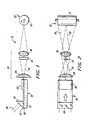
- Figures 1 and 2 disclose an. electro-optic line printer 11 comprising light valve 50 for exposing a photosensitive recording medium 13 in an image configuration.
- the recording medium 13 is depicted as being a photoconductively coated xerographic drum 14 which is rotated (by means not shown) in the direction of the arrow. It will be evident, however, that there are other xerographic and non-xerographic recording media that could be used, including photoconductively coated xerographic belts and plates, as well as photosensitive film and coated paper which may be supplied as web or cut sheet stock.
- the recording medium 13 should, therefore, be visualized in the generalized case as being a photosensitive medium which is exposed in an image configuration. while advancing, in a cross line or line pitch direction relative to the light valve 50.
- the light valve disclosed in said co- pending. application No.: 81304270.2 as hereinabove set forth operates in a TIR (Total Internal Reflective) mode.
- the present application includes a light valve 50 wherein the electro-optic interaction is not in the TIR mode, but with a light guided in thin film 54.
- the basic valve 50 utilizes a. thin electro-optic layer on a substrate 52, with the. index of refraction of the film being higher than the substrate so that light can be guided in film 54.
- Substrate 52 could comprise lithium niobate with titanium in-diffused or lithium oxide out-diffused..
- Dotted line 57 represents the rough boundary of said diffusion layer.
- the solid line 55 upper level of film 54 could comprise an insulating layer of silicon dioxide to avoid spurious amplitude and phase modulation of the light.
- a laser beam 48 is caused to be guided in the film by means of any one of many prior art techniques such as by coupling to the thin film 54 by prism 56, or it could be by the techniques of grating coupling, butt coupling, or film integration with a diode laser. Beam 48 is expanded sideways either before or after coupling into the film so that a sheet of collimated light is provided.. This light 48 is guided beneath an array of individually addressable electrodes (60a, 60n), and groundplane electrodes (62a, 62n) which is identical to the array set forth in the aforementioned co-pending application No. 81304270.2.
- the light diffracted by this electrode set is reimaged onto the recording medium 13 with the zero order diffracted light blocked out by the the zero order stop 35; so that each pair of electrodes (60a, 60n) - (62a, 62n) acts as a light modulator for one picture element on each line of the output printed image.
- the zero order diffracted light could be reimaged and the diffracted light blocked out.
- the light travels through this thin film beneath the drive electrodes 58 and illuminates substantially the full width of the thin film at the location of the electrode.
- the light beam 48 is modulated while passing underneath the drive electrodes with the data samples applied to the electrode pairs (60a, 60n) -(62a, 62n).
- successive sets of digital or analog data samples which represent respective collections of picture elements for successive lines of the image, are sequentially applied to the electrode pairs (60a, 60n) - (62a, 62n).
- Activation of the electrodes selectively changes the refractive index of the thin film substrate 54, causing a predetermined diffraction effect which modulates the light beam 24. Consequently, the phase front of the light beam 24 is serially and spatially modulated in accordance with the data samples for successive lines of the image as the light beam 24 passes through the region directly below the electrode structure 58 of the electro-optic element 50.
- the illustrated imaging opics 31 include a field lens 34 for focusing the zero order diffraction components 32 of the phase front modulated light beam 24 onto a central stop 35 and an imaging lens 36 for collecting the scattered higher order diffraction components onto the light valve image plane defined by the recording medium 13.
- the field lens 34 is optically aligned between the electro- optic element 50 and the stop 35 so that substantially all of the zero order components 32 of the light beam 24 are blocked by the stop 35.
- the higher order diffraction components of the light beam 24 scatter around the stop 35 and are collected by the imaging lens 36 which, in turn, focusses them onto the recording medium 13.
- other readout optics could be used to convert the phase front or polarization modulated light beam provided by the electro-optic element 50 into a light beam having a correspondingly modulated intensity profile as both set forth, for example, in said co-pending application and in this application.
- each pair of electrodes (60a, 60n) - (62a, 62n) cooperates with the electro-optic element 50 and . the phase modulated sensitive readout optics 36 to effectively define a local modulator for creating a picture element at a unique, spatially pre - determined position along each. line of the image. Accordingly, the number of electrode pairs (60a, 60n) - (62a, 62n) determines the number of picture elements that can be printed on each line of the image. By sequentially applying successive sets of data samples. to 'these local modulators while the recording medium 13 is advancing in a cross line direction relative to the light valve 50, successive lines of the image are printed.
- the drive electronics for the invention set forth herein are the same as that set forth above in the said co-pending application. If LSI (Large Scale Integration) technology is used for fabrication of the light valve 50, the coupling between the silicon drive electronics and the electrode pattern is solved as set forth in copending European Patent Application No 81304272.8. In the most likely device design, said coupling is achieved with the electrodes fabricated on the silicon chip 58 and pressed against the top of thin film 54 as shown in Figure 1, so that the fringing field of the electrodes (60a, 60n) - (62a, 62n) is coupled into the thin film 54.
- LSI Large Scale Integration
- the film 54 could be overcoated with a thin dielectric layer 55 to prevent unwanted spurious modulation of the light beam 24.
- an alternative choice for said drive electronics could use thin film transducer technology to build the electronics directly on the integrated optics substrate.
- a thin film multi-gate light valve could be fabricated by magnetron sputtering of a thin film electro-optic overcoating of, for example, zinc oxide (ZnO) onto a silicon dioxide (Si0 2 ) outer layer of an electrode bearing LSI driver and/or onto an electrode (gold, copper, titanium, or tungsten) metallization layer of such a driver.
- ZnO zinc oxide
- Si0 2 silicon dioxide
- Au gold, copper, titanium, or tungsten
Abstract
Description
- This invention- relates to an electro-optic line printer. Such a printer typically includes a multi-gate light valve for phase front or polarization modulating a sheet like, collimated light beam in accordance with input data samples of finite duration representing individual picture elements of an image, and phase or polarization sensitive optics for imaging the modulated light beam onto a photosensitive recording medium as said recording medium advances in a cross line direction relative to said light valve, whereby said recording medium is exposed in an image configuration.
- An example of this kind of line printer is described in European Patent Publication No. 0021754. Also see "Light Gates Give Data Recorder Improved Hardcopy Resolution", Electronic Design, July 19 1979, Pages 31-32; "Polarizing Filters Plot Analog Waveforms", Machine Design, Volume 51, Number 17, July 26, 1979,
Page 62; and "Data Recorder Eliminates Problem of Linearity", Design News, February 4 1980, pages 56-57. - Copending European Patent Application No 81304270.2 discloses the support optics and electronics for incorporating a multi-gate light valve into a line printer.
- In co-pending application No. 81304270.2, it is disclosed that almost any optically transparent electro-optic material can be used as the electro-optic element of such a light valve as disclosed herein. Presently, the most promising materials appear to be LiNbO3 and LiTa03, but there are other materials which qualify for consideration, including BSN, KDP, Ba2NaNb5O15 and PLZT. In any event, the electrodes of such a light valve are intimately coupled to the electro-optic element and are distributed in non-overlapping relationship widthwise of the electro-optic element (i.e. orthogonally relative to its optical axis), typically on equidistantly separated centers so that there is a generally uniform interelectrode gap spacing.
- To perform line printing with a multi-gate light valve of the foregoing type, a photosensitive recording medium such as a xerographic photoreceptor is exposed in an image configuration as it advances in a cross line direction (i.e., a line pitch direction) relative to the light valve. More particularly, to carry. out the exposure process, a sheetlike collimated light beam is transmitted through the electro-optic element of the light valve, either along its optical axis for straight through transmission or at a slight angle relative to that axis for total internal reflection (TIR). Furthermore, successive sets of digital bits or analog signal samples (hereinafter collectively referred to as "data samples"), which represent respective collections of picture elements or pixels for successive lines of the image, are sequentially applied to the electrodes. As a result, localized electric bulk or fringe fields are created within the electro-optic element in the immediate vicinity of any electrodes to which non-reference level data samples are applied. These fields, in turn, cause localized variations in the refractive index of the electro- optic element within an interaction region (that is, a light beam illuminated region of the electro-optic element which is subject to being penetrated by the electric fields). Thus, the phase front or polarization of the light beam is modulated in accordance with the data samples applied to the electrodes as the light beam passes through the interaction region.
- The present invention is intended to provide an alternative form of light modulator for use in such an electro-optic line printer. The invention is characterised in that the light valve comprises a substrate containing an optically transmissive electro-optic film, drive electrodes, in the form of a plurality of individually addressable electrodes formed in said electro-optic film such that when said light beam is guided by said optically transmissive electro-optic element, said light completely passes under said drive electrodes, said individually addressable electrodes creating electric fringe fields within said electrooptic element to phase front or polarization modulate said light beam.
- The present invention relates to a thin film light modulator for use in such an electro-optic line printer. According to the present
- The light valve utilizes a thin electro-optic film on a substrate, with the index of refraction of the film being higher than the substrate so that the light can be guided in it. A laser beam is caused to be guided in the film through one of the many ways noted in the literature. This beam is expanded sideways either before or after coupling into the film so that a sheet of collimated light is provided. This light is guided beneath an array of electrodes identical. to the array described in co- pending application No. 81304270.2 which consists of an extended set of individually addressed metal fingers.. As set forth in said co-pending application, the light diffracted by this electrode set is reimaged onto the recording medium, with the zero order diffracted light blocked out, so that each electrode acts as a light modulator for one picture element on the output. Alternatively, the zero order is reimaged and diffracted light blocked out. By applying each bit of a serial stream of data to each electrode after serial to parallel conversion, a line recording of the data is achieved.
- For a more complete understanding of the invention, reference may be had to the following detailed description of the invention in conjunction with the drawings wherein:
- Figure 1 is a schematic side view of a straight through electro-optic line printer constructed in accordance with the present invention;
- Figure 2 is a schematic top plan view of the electro-optic line printer shown in Figure 1; and
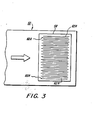
- Figure 3 is an enlarged partially cutaway plan view of the light valve of the line printer of Figures 1 and 2.
- Figures 1 and 2 disclose an. electro-
optic line printer 11 comprisinglight valve 50 for exposing aphotosensitive recording medium 13 in an image configuration. Therecording medium 13 is depicted as being a photoconductively coatedxerographic drum 14 which is rotated (by means not shown) in the direction of the arrow. It will be evident, however, that there are other xerographic and non-xerographic recording media that could be used, including photoconductively coated xerographic belts and plates, as well as photosensitive film and coated paper which may be supplied as web or cut sheet stock. Therecording medium 13 should, therefore, be visualized in the generalized case as being a photosensitive medium which is exposed in an image configuration. while advancing, in a cross line or line pitch direction relative to thelight valve 50. The light valve disclosed in said co- pending. application No.: 81304270.2 as hereinabove set forth, operates in a TIR (Total Internal Reflective) mode. The present application includes alight valve 50 wherein the electro-optic interaction is not in the TIR mode, but with a light guided inthin film 54. Thebasic valve 50 utilizes a. thin electro-optic layer on asubstrate 52, with the. index of refraction of the film being higher than the substrate so that light can be guided infilm 54.Substrate 52 could comprise lithium niobate with titanium in-diffused or lithium oxide out-diffused.. Dotted line 57 represents the rough boundary of said diffusion layer. Thesolid line 55 upper level offilm 54 could comprise an insulating layer of silicon dioxide to avoid spurious amplitude and phase modulation of the light. Alaser beam 48 is caused to be guided in the film by means of any one of many prior art techniques such as by coupling to thethin film 54 byprism 56, or it could be by the techniques of grating coupling, butt coupling, or film integration with a diode laser. Beam 48 is expanded sideways either before or after coupling into the film so that a sheet of collimated light is provided.. Thislight 48 is guided beneath an array of individually addressable electrodes (60a, 60n), and groundplane electrodes (62a, 62n) which is identical to the array set forth in the aforementioned co-pending application No. 81304270.2. As in the TIR multi-gate light valve, the light diffracted by this electrode set is reimaged onto therecording medium 13 with the zero order diffracted light blocked out by the the zeroorder stop 35; so that each pair of electrodes (60a, 60n) - (62a, 62n) acts as a light modulator for one picture element on each line of the output printed image. As an alternative, the zero order diffracted light could be reimaged and the diffracted light blocked out. By sequentially applying the bits of a serial stream of data to each corresponding electrode, as set forth in said co-pending application, a line recording can be achieved. - In operation, a sheet-like collimated beam of light 4& from a: suitable source, such as a laser (not shown), is transmitted through
prism 56 onto thethin film 54 of thevalve 50. The light travels through this thin film beneath thedrive electrodes 58 and illuminates substantially the full width of the thin film at the location of the electrode. Thelight beam 48 is modulated while passing underneath the drive electrodes with the data samples applied to the electrode pairs (60a, 60n) -(62a, 62n). - More particularly, to modulate the
light beam 48, successive sets of digital or analog data samples, which represent respective collections of picture elements for successive lines of the image, are sequentially applied to the electrode pairs (60a, 60n) - (62a, 62n). Activation of the electrodes selectively changes the refractive index of thethin film substrate 54, causing a predetermined diffraction effect which modulates thelight beam 24. Consequently, the phase front of thelight beam 24 is serially and spatially modulated in accordance with the data samples for successive lines of the image as thelight beam 24 passes through the region directly below theelectrode structure 58 of the electro-optic element 50. - To expose the
recording medium 13 in an image configuration, there suitably are..Schlieren central darkfield imaging optics 31 which are optically aligned between the electro-optic valve 50 and therecording medium 13 for imaging thelight beam 24 onto therecording medium 13. Theimaging optics 31 convert the spatial phase front modulation into a correspondingly modulated intensity profile and provide any magnification that is required to obtain an image of a desired width. To accomplish that, the illustratedimaging opics 31 include afield lens 34 for focusing the zeroorder diffraction components 32 of the phase front modulatedlight beam 24 onto acentral stop 35 and animaging lens 36 for collecting the scattered higher order diffraction components onto the light valve image plane defined by therecording medium 13. Thefield lens 34 is optically aligned between the electro-optic element 50 and thestop 35 so that substantially all of the zeroorder components 32 of thelight beam 24 are blocked by thestop 35. The higher order diffraction components of thelight beam 24 scatter around thestop 35 and are collected by theimaging lens 36 which, in turn, focusses them onto therecording medium 13. Of course, other readout optics could be used to convert the phase front or polarization modulated light beam provided by the electro-optic element 50 into a light beam having a correspondingly modulated intensity profile as both set forth, for example, in said co-pending application and in this application. As indicated in Figure 2 bylines 39, each pair of electrodes (60a, 60n) - (62a, 62n) cooperates with the electro-optic element 50 and . the phase modulatedsensitive readout optics 36 to effectively define a local modulator for creating a picture element at a unique, spatially pre- determined position along each. line of the image. Accordingly, the number of electrode pairs (60a, 60n) - (62a, 62n) determines the number of picture elements that can be printed on each line of the image. By sequentially applying successive sets of data samples. to 'these local modulators while therecording medium 13 is advancing in a cross line direction relative to thelight valve 50, successive lines of the image are printed. - The drive electronics for the invention set forth herein are the same as that set forth above in the said co-pending application. If LSI (Large Scale Integration) technology is used for fabrication of the
light valve 50, the coupling between the silicon drive electronics and the electrode pattern is solved as set forth in copending European Patent Application No 81304272.8. In the most likely device design, said coupling is achieved with the electrodes fabricated on thesilicon chip 58 and pressed against the top ofthin film 54 as shown in Figure 1, so that the fringing field of the electrodes (60a, 60n) - (62a, 62n) is coupled into thethin film 54. If necessary, as set forth in said copending application, thefilm 54 could be overcoated with athin dielectric layer 55 to prevent unwanted spurious modulation of thelight beam 24. Further, instead of external electronics, an alternative choice for said drive electronics could use thin film transducer technology to build the electronics directly on the integrated optics substrate. - As another alternative, a thin film multi-gate light valve could be fabricated by magnetron sputtering of a thin film electro-optic overcoating of, for example, zinc oxide (ZnO) onto a silicon dioxide (Si02) outer layer of an electrode bearing LSI driver and/or onto an electrode (gold, copper, titanium, or tungsten) metallization layer of such a driver.
Claims (7)
the light valve (50) comprises a substrate (52) containing an optically transmissive electro-optic film (54), drive electrodes (60, 62) in the form of a plurality of individually addressable electrodes formed in said electro-optic film (54) such that when said light beam is guided by said optically transmissive electro-optic element, said light completely passes under said drive electrodes, said individually addressable electrodes creating electric fringe fields within said electrooptic element to phase front or polarization modulate said light beam.
said ground plane electrodes are intimately coupled to and distributed across said electro-optic film in alternating paired relationship with said individually addressable electrodes.
Applications Claiming Priority (2)
| Application Number | Priority Date | Filing Date | Title |
|---|---|---|---|
| US06/224,243 US4421387A (en) | 1981-01-12 | 1981-01-12 | Extended thin film light modulator/scanner |
| US224243 | 1981-01-12 |
Publications (2)
| Publication Number | Publication Date |
|---|---|
| EP0056334A1 true EP0056334A1 (en) | 1982-07-21 |
| EP0056334B1 EP0056334B1 (en) | 1986-04-02 |
Family
ID=22839849
Family Applications (1)
| Application Number | Title | Priority Date | Filing Date |
|---|---|---|---|
| EP82300161A Expired EP0056334B1 (en) | 1981-01-12 | 1982-01-12 | Thin film electro-optic line printer |
Country Status (5)
| Country | Link |
|---|---|
| US (1) | US4421387A (en) |
| EP (1) | EP0056334B1 (en) |
| JP (1) | JPS57156272A (en) |
| CA (1) | CA1184589A (en) |
| DE (1) | DE3270194D1 (en) |
Cited By (5)
| Publication number | Priority date | Publication date | Assignee | Title |
|---|---|---|---|---|
| EP0123425A1 (en) * | 1983-04-11 | 1984-10-31 | Xerox Corporation | Multi-channel electro-optic printer |
| EP0182675A2 (en) * | 1984-11-23 | 1986-05-28 | Michel Moulin | Photocomposition method and machine |
| EP0198380A2 (en) * | 1985-04-08 | 1986-10-22 | Fuji Photo Film Co., Ltd. | Light beam scanning apparatus and read-out or recording apparatus using the same |
| US4793697A (en) * | 1986-08-04 | 1988-12-27 | Motorola, Inc. | PLZT shutter with minimized space charge degradation |
| US4819018A (en) * | 1985-02-22 | 1989-04-04 | Moyroud Louis M | High-speed broad-brush laser photocomposition |
Families Citing this family (11)
| Publication number | Priority date | Publication date | Assignee | Title |
|---|---|---|---|---|
| JPS57142664A (en) * | 1981-02-27 | 1982-09-03 | Canon Inc | Information recorder |
| US4577932A (en) * | 1984-05-08 | 1986-03-25 | Creo Electronics Corporation | Multi-spot modulator using a laser diode |
| US4591260A (en) * | 1984-09-04 | 1986-05-27 | Xerox Corporation | Imaging system utilizing an electro-optic device |
| US4750815A (en) * | 1984-11-16 | 1988-06-14 | Hitachi, Ltd. | Method and apparatus for generating optical information |
| US4902088A (en) * | 1986-03-25 | 1990-02-20 | Apa Optics, Inc. | Integrated optic device for laser beam scanning |
| US4801184A (en) * | 1987-06-15 | 1989-01-31 | Eastman Kodak Company | Integrated optical read/write head and apparatus incorporating same |
| US4803498A (en) * | 1987-07-13 | 1989-02-07 | Blaser Industries, Incorporated | Laser printer recording system |
| US4780732A (en) * | 1988-03-21 | 1988-10-25 | Xerox Corporation | Dual interaction TIR modulator |
| US5052771A (en) * | 1990-12-21 | 1991-10-01 | Eastman Kodak Company | Integrated electro-optical scanner |
| JPH05134275A (en) * | 1991-11-12 | 1993-05-28 | Hitachi Koki Co Ltd | Light control element |
| US5521748A (en) * | 1994-06-16 | 1996-05-28 | Eastman Kodak Company | Light modulator with a laser or laser array for exposing image data |
Citations (5)
| Publication number | Priority date | Publication date | Assignee | Title |
|---|---|---|---|---|
| US3837728A (en) * | 1973-09-26 | 1974-09-24 | Bell Telephone Labor Inc | Injected carrier guided wave deflector |
| US3904270A (en) * | 1974-02-27 | 1975-09-09 | United Aircraft Corp | Integrated optical signal processing system |
| DE2607793A1 (en) * | 1975-06-17 | 1976-12-30 | Ibm | MAGNETO-OPTICAL LIGHT DEFLECTOR |
| US4047795A (en) * | 1974-11-22 | 1977-09-13 | The United States Of America As Represented By The Secretary Of The Navy | Optical integrated circuit laser beam scanner |
| GB1543485A (en) * | 1976-07-02 | 1979-04-04 | Thomson Csf | Magneto optical deflector |
Family Cites Families (7)
| Publication number | Priority date | Publication date | Assignee | Title |
|---|---|---|---|---|
| US3810688A (en) * | 1973-05-21 | 1974-05-14 | A Ballman | Optical waveguiding devices using monocrystalline materials of the sillenite family of bismuth oxides |
| US4111523A (en) * | 1973-07-23 | 1978-09-05 | Bell Telephone Laboratories, Incorporated | Thin film optical waveguide |
| US3990775A (en) * | 1973-07-23 | 1976-11-09 | Bell Telephone Laboratories, Incorporated | Thin-film optical waveguide |
| US3877781A (en) * | 1974-01-16 | 1975-04-15 | Bell Telephone Labor Inc | Electro-optical thin-film device |
| US3877782A (en) * | 1974-01-23 | 1975-04-15 | Bell Telephone Labor Inc | Electro-optical thin film device |
| DE2443733A1 (en) * | 1974-09-12 | 1976-03-25 | Siemens Ag | ARRANGEMENT FOR MODULATION OF LIGHT |
| US4106848A (en) * | 1975-10-10 | 1978-08-15 | Xerox Corporation | Elastomer wave guide optical modulators |
-
1981
- 1981-01-12 US US06/224,243 patent/US4421387A/en not_active Expired - Lifetime
- 1981-12-08 CA CA000391762A patent/CA1184589A/en not_active Expired
- 1981-12-22 JP JP56207943A patent/JPS57156272A/en active Pending
-
1982
- 1982-01-12 DE DE8282300161T patent/DE3270194D1/en not_active Expired
- 1982-01-12 EP EP82300161A patent/EP0056334B1/en not_active Expired
Patent Citations (5)
| Publication number | Priority date | Publication date | Assignee | Title |
|---|---|---|---|---|
| US3837728A (en) * | 1973-09-26 | 1974-09-24 | Bell Telephone Labor Inc | Injected carrier guided wave deflector |
| US3904270A (en) * | 1974-02-27 | 1975-09-09 | United Aircraft Corp | Integrated optical signal processing system |
| US4047795A (en) * | 1974-11-22 | 1977-09-13 | The United States Of America As Represented By The Secretary Of The Navy | Optical integrated circuit laser beam scanner |
| DE2607793A1 (en) * | 1975-06-17 | 1976-12-30 | Ibm | MAGNETO-OPTICAL LIGHT DEFLECTOR |
| GB1543485A (en) * | 1976-07-02 | 1979-04-04 | Thomson Csf | Magneto optical deflector |
Cited By (7)
| Publication number | Priority date | Publication date | Assignee | Title |
|---|---|---|---|---|
| EP0123425A1 (en) * | 1983-04-11 | 1984-10-31 | Xerox Corporation | Multi-channel electro-optic printer |
| EP0182675A2 (en) * | 1984-11-23 | 1986-05-28 | Michel Moulin | Photocomposition method and machine |
| EP0182675A3 (en) * | 1984-11-23 | 1987-12-02 | Michel Moulin | Photocomposition method and machine |
| US4819018A (en) * | 1985-02-22 | 1989-04-04 | Moyroud Louis M | High-speed broad-brush laser photocomposition |
| EP0198380A2 (en) * | 1985-04-08 | 1986-10-22 | Fuji Photo Film Co., Ltd. | Light beam scanning apparatus and read-out or recording apparatus using the same |
| EP0198380A3 (en) * | 1985-04-08 | 1988-10-19 | Fuji Photo Film Co., Ltd. | Light beam scanning apparatus and read-out or recording apparatus using the same |
| US4793697A (en) * | 1986-08-04 | 1988-12-27 | Motorola, Inc. | PLZT shutter with minimized space charge degradation |
Also Published As
| Publication number | Publication date |
|---|---|
| JPS57156272A (en) | 1982-09-27 |
| EP0056334B1 (en) | 1986-04-02 |
| CA1184589A (en) | 1985-03-26 |
| DE3270194D1 (en) | 1986-05-07 |
| US4421387A (en) | 1983-12-20 |
Similar Documents
| Publication | Publication Date | Title |
|---|---|---|
| US4367925A (en) | Integrated electronics for proximity coupled electro-optic devices | |
| CA1171508A (en) | Proximity coupled electro-optic devices | |
| EP0062522B1 (en) | Proximity-coupled electro-optic devices | |
| US4538883A (en) | Conformable electrodes for proximity coupled electro-optic devices | |
| EP0056334B1 (en) | Thin film electro-optic line printer | |
| US4724467A (en) | Light blocking stop for electro-optic line printers | |
| US4636039A (en) | Nonuniformity of fringe field correction for electro-optic devices | |
| EP0550189B1 (en) | Electrooptic TIR light modulator image bar having multiple electrodes per pixel | |
| US4450459A (en) | Differential encoding for fringe field responsive electro-optic line printers | |
| EP0087970B1 (en) | Linear modulators | |
| EP0061926B1 (en) | Multigate light valve for electro-optic line printers having non telecentric imaging systems | |
| US4370029A (en) | Dielectric interface for proximity coupled electro-optic devices | |
| EP0057977B1 (en) | Electro-optic line printer | |
| US4389659A (en) | Electro-optic line printer | |
| US4369457A (en) | Reverse polarity differential encoding for fringe field responsive electro-optic line printers | |
| US4437106A (en) | Method and means for reducing illumination nulls in electro-optic line printers | |
| US4415915A (en) | Multilayer interleaved electrodes for multigate light valves | |
| US4380373A (en) | Conformable proximity coupled electro-optic devices | |
| US4482215A (en) | Mechanical interface for proximity coupled electro-optic devices | |
| EP0048595B1 (en) | Line printers | |
| EP0051356B1 (en) | Electro-optic devices | |
| EP0072124B1 (en) | Light-modulating device comprising a multigate light valve | |
| JPH0328713B2 (en) |
Legal Events
| Date | Code | Title | Description |
|---|---|---|---|
| PUAI | Public reference made under article 153(3) epc to a published international application that has entered the european phase |
Free format text: ORIGINAL CODE: 0009012 |
|
| AK | Designated contracting states |
Designated state(s): DE FR GB IT |
|
| 17P | Request for examination filed |
Effective date: 19821222 |
|
| R17P | Request for examination filed (corrected) |
Effective date: 19821208 |
|
| GRAA | (expected) grant |
Free format text: ORIGINAL CODE: 0009210 |
|
| AK | Designated contracting states |
Kind code of ref document: B1 Designated state(s): DE FR GB IT |
|
| REF | Corresponds to: |
Ref document number: 3270194 Country of ref document: DE Date of ref document: 19860507 |
|
| ET | Fr: translation filed | ||
| ITF | It: translation for a ep patent filed |
Owner name: MODIANO & ASSOCIATI S.R.L. |
|
| PLBE | No opposition filed within time limit |
Free format text: ORIGINAL CODE: 0009261 |
|
| STAA | Information on the status of an ep patent application or granted ep patent |
Free format text: STATUS: NO OPPOSITION FILED WITHIN TIME LIMIT |
|
| 26N | No opposition filed | ||
| ITTA | It: last paid annual fee | ||
| PGFP | Annual fee paid to national office [announced via postgrant information from national office to epo] |
Ref country code: FR Payment date: 19990111 Year of fee payment: 18 |
|
| PGFP | Annual fee paid to national office [announced via postgrant information from national office to epo] |
Ref country code: GB Payment date: 19990114 Year of fee payment: 18 |
|
| PGFP | Annual fee paid to national office [announced via postgrant information from national office to epo] |
Ref country code: DE Payment date: 19990115 Year of fee payment: 18 |
|
| PG25 | Lapsed in a contracting state [announced via postgrant information from national office to epo] |
Ref country code: GB Free format text: LAPSE BECAUSE OF NON-PAYMENT OF DUE FEES Effective date: 20000112 |
|
| GBPC | Gb: european patent ceased through non-payment of renewal fee |
Effective date: 20000112 |
|
| PG25 | Lapsed in a contracting state [announced via postgrant information from national office to epo] |
Ref country code: FR Free format text: LAPSE BECAUSE OF NON-PAYMENT OF DUE FEES Effective date: 20000929 |
|
| PG25 | Lapsed in a contracting state [announced via postgrant information from national office to epo] |
Ref country code: DE Free format text: LAPSE BECAUSE OF NON-PAYMENT OF DUE FEES Effective date: 20001101 |
|
| REG | Reference to a national code |
Ref country code: FR Ref legal event code: ST |