EP0056191A2 - Integrated injection logic - Google Patents
Integrated injection logic Download PDFInfo
- Publication number
- EP0056191A2 EP0056191A2 EP81306108A EP81306108A EP0056191A2 EP 0056191 A2 EP0056191 A2 EP 0056191A2 EP 81306108 A EP81306108 A EP 81306108A EP 81306108 A EP81306108 A EP 81306108A EP 0056191 A2 EP0056191 A2 EP 0056191A2
- Authority
- EP
- European Patent Office
- Prior art keywords
- semiconductor region
- semiconductor
- transistor
- conductivity type
- integrated injection
- Prior art date
- Legal status (The legal status is an assumption and is not a legal conclusion. Google has not performed a legal analysis and makes no representation as to the accuracy of the status listed.)
- Granted
Links
Images

Classifications
-
- H—ELECTRICITY
- H01—ELECTRIC ELEMENTS
- H01L—SEMICONDUCTOR DEVICES NOT COVERED BY CLASS H10
- H01L27/00—Devices consisting of a plurality of semiconductor or other solid-state components formed in or on a common substrate
- H01L27/02—Devices consisting of a plurality of semiconductor or other solid-state components formed in or on a common substrate including semiconductor components specially adapted for rectifying, oscillating, amplifying or switching and having at least one potential-jump barrier or surface barrier; including integrated passive circuit elements with at least one potential-jump barrier or surface barrier
- H01L27/0203—Particular design considerations for integrated circuits
- H01L27/0214—Particular design considerations for integrated circuits for internal polarisation, e.g. I2L
- H01L27/0229—Particular design considerations for integrated circuits for internal polarisation, e.g. I2L of bipolar structures
- H01L27/0233—Integrated injection logic structures [I2L]
-
- H—ELECTRICITY
- H03—ELECTRONIC CIRCUITRY
- H03K—PULSE TECHNIQUE
- H03K19/00—Logic circuits, i.e. having at least two inputs acting on one output; Inverting circuits
- H03K19/02—Logic circuits, i.e. having at least two inputs acting on one output; Inverting circuits using specified components
- H03K19/08—Logic circuits, i.e. having at least two inputs acting on one output; Inverting circuits using specified components using semiconductor devices
- H03K19/082—Logic circuits, i.e. having at least two inputs acting on one output; Inverting circuits using specified components using semiconductor devices using bipolar transistors
- H03K19/091—Integrated injection logic or merged transistor logic
-
- Y—GENERAL TAGGING OF NEW TECHNOLOGICAL DEVELOPMENTS; GENERAL TAGGING OF CROSS-SECTIONAL TECHNOLOGIES SPANNING OVER SEVERAL SECTIONS OF THE IPC; TECHNICAL SUBJECTS COVERED BY FORMER USPC CROSS-REFERENCE ART COLLECTIONS [XRACs] AND DIGESTS
- Y10—TECHNICAL SUBJECTS COVERED BY FORMER USPC
- Y10S—TECHNICAL SUBJECTS COVERED BY FORMER USPC CROSS-REFERENCE ART COLLECTIONS [XRACs] AND DIGESTS
- Y10S257/00—Active solid-state devices, e.g. transistors, solid-state diodes
- Y10S257/914—Polysilicon containing oxygen, nitrogen, or carbon, e.g. sipos
Definitions
- the present invention relates to an integrated injection logic.
- I 2 L An integrated injection logic (I 2 L) does not require isolation between semiconductor elements even though the integrated injection logic is a bipolar transistor. Therefore, such a semiconductor device is highly integrated. Further, since a lateral pnp transistor is used as a current source or load, power consumption is greatly reduced.
- An integrated injection logic (to be referred to as an 1 2 L hereinafter) comprises an n +- type semiconductor substrate, an n-type epitaxial layer which is formed on the semiconductor substrate, a p-type injector region which is formed in this epitaxial layer, a p-type layer which is formed in the epitaxial layer, and a plurality of n-type regions which are formed in the p-type layer.
- minority carriers are excessively accumulated in the n-type expitaxial layer and the p-type layer which is formed in the n-type epitaxial layer when the I 2 L operates, reducing the switching speed of the device.
- an integrated injection logic in which a first semiconductor region of the same conductivity type as.a base region is formed in the vicinity of the base region of a bipolar transistor which functions as an inverter of the integrated injection logic, and a second semiconductor region whose conductivity type is opposite to that of the base region and which is formed in the base region is connected to this first semiconductor region.
- the minority carriers may be eliminated in accordance with the potential difference.
- Fig. 1 is a circuit diagram of an I 2 L according to the present invention.
- the 1 2L comprises a first transistor Trl which has a plurality of output ends OUT and functions as an inverter, a second transistor Tr2 which functions as a current source and load for the first transistor Trl, and a third transistor Tr3 connected to the first transistor Trl.
- the emitter of the first transistor Trl of the npn type is grounded, the base thereof is connected to an input signal supply end IN, and the collector thereof functions as the output ends.
- the emitter of the second transistor Tr2 of the pnp type is connected to a power source voltage supply end Vee, the base thereof is grounded, and the collector thereof is connected to the base of the first transistor Trl.
- the emitter of the third transistor Tr3 of the pnp type is connected to one of the output ends OUT of the first transistor Trl, the base thereof is grounded, and the collector thereof is connected to the base of the first transistor Trl.
- the third transistor Tr3 operates to eliminate excessive minority carriers which are stored in the base and emitter of the first transistor Trl in response to the operation of the first transistor Trl.
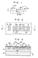
- Figs. 2 and 3 show detailed arrangements of the device of the circuit diagram shown in Fig. 1, in which Fig. 2 is a plan view of the device, and Fig. 3 is as selectionnal view thereof along the line III - III of Fig. 2.
- An n-type epitaxial layer 12 is formed on an n +- type semiconductor substrate 10.
- a first semiconductor region 14 of p + conductivity type, a second semiconductor region 16 of p + conductivity type, and a third semiconductor region 18 of p + conductivity type are formed in the n-type epitaxial layer 12.
- Three fourth semiconductor regions 20a, 20b and 20c of n + conductivity type are formed in the first semiconductor region 14.
- the first transistor Trl comprises the epitaxial layer 12, the first semiconductor region 14 and the fourth semiconductor regions 20a and 20b.
- the epitaxial layer 12 functions as the emitter of the first transistor Trl, the first semiconductor region 14 functions as the base thereof, and the fourth semiconductor layers 20a and 20b function as the collector thereof.
- the second transistor Tr2 comprises the second semiconductor region 16, the epitaxial layer 12 and the first semiconductor region 14.
- the second semiconductor region 16 functions as the emitter of the second transistor Tr2, the epitaxial layer 12 functions as the base thereof, and the first semiconductor region 14 functions as the collector thereof.
- the third transistor Tr3 comprises the first semiconductor region 14, the epitaxial layer 12, and the third.semiconductor region 18.
- the first semiconductor region 14 functions as the collector of the third transistor Tr3, the epitaxial layer 12 functions as the base thereof, and the third semiconductor region 18 functions as the emitter thereof.
- An Si0 2 film 22 in which contact holes are selectively formed is formed on the surface of the semconductor substrate.
- the second semiconductor region 16 is connected to the power source voltage supply end Vee through the contact hole, and the first semiconductor region 14 is connected to the input signal supply end IN through the contact hole, and the fourth semiconductor regions 20a and 20b are respectively connected to the output ends OUT.
- the third semiconductor region 18 is connected to the fourth semiconductor region 20c through an electrode wiring 24.
- a delay time tpd of the I 2 L is defined by the following equation (Fransois M. Klaassen, "Device Physics of Integrated Injection Logic", IEEE Transaction Electron Devices, Vol. ED 22, March 1975, pp. 145 - 152)
- the effective current amplification factor ßeff and the cut-off frequency fT of the transistor Trl are defined by the following equations.
- ßupo is the current amplification factor of the transistor Trl when the injector (second transistor Tr2) is open
- ßi is the reverse current amplification factor of the injector
- ic is the collector current of the first transistor Trl
- Qepi is the number of minority carriers stored in the epitaxial layer 12.
- the reverse current amplification factor ßi of the injector is increased. Further, since the minority carriers generated in the epitaxial layer 12 are absorbed in the emitter region 18 of the-third transistor Tr3, the number Qepi of minority carriers is reduced. According to equation (2), the effective current amplification factor ⁇ eff of the first transistor Trl is reduced. The cut-off frequency fT of the first transistor Trl increases according to equation (3). As a result, the delay time tpd of the I 2 L is shortened according to equation (1).
- FIG. 4 An I 2 L of a second embodiment of the present invention will be described with reference to Fig. 4.
- the 1 2 L according to this embodiment is the same as that shown in Figs. 2 and 3 except that the emitter of the third transistor Tr3 is arranged to surround the first transistor Trl.
- the same reference numerals in Fig. 4 denote the same parts as in Figs. 2 and 3, and the detailed description will be omitted. With this arrangement, the excessive carriers are effectively removed so that the switching speed of the I 2 L is further improved.
- the I 2 L of a third embodiment of the present invention will be described with reference to Fig. 5.
- the I 2 L of this embodiment is the same as that in Fig. 3, except that the first semiconductor region 14 which functions as the base of the first transistor Trl is formed by a first semiconductor layer 26 of p conductivity type and a second semiconductor layer 28 of p + conductivity type, in which the second semiconductor layer 28 is connected to the input signal supply end IN and arranged to surround the fourth semiconductor regions 20a, 20b and 20c.
- the same reference numerals in Fig. 5 denote the same parts as in Fig. 3, and the detailed description thereof will be omitted. With this arrangement, the minority carriers are effectively eliminated so that the switching speed of the I 2 L is greatly improved.
- FIG. 6 An I 2 L of a fourth embodiment of the present invention will be described with reference to Fig. 6.
- the I 2 L in this embodiment is the same as that shown in Fig. 5, except that an n-type well layer 30 is selectively formed in the semiconductor substrate 10 instead of the n-type epitaxial layer in order to form the emitter region of higher concentration.
- the same reference numerals in Fig. 6 denote the same parts as in Fig. 5, and the detailed description thereof will be omitted.
- the same effect as in the previous embodiments is accomplished, in which the minority carriers are effectively eliminated and the switching operation of the I 2 L is accomplished with high speed.
Abstract
Description
- The present invention relates to an integrated injection logic.
- An integrated injection logic (I2L) does not require isolation between semiconductor elements even though the integrated injection logic is a bipolar transistor. Therefore, such a semiconductor device is highly integrated. Further, since a lateral pnp transistor is used as a current source or load, power consumption is greatly reduced.
- An integrated injection logic (to be referred to as an 12L hereinafter) comprises an n+-type semiconductor substrate, an n-type epitaxial layer which is formed on the semiconductor substrate, a p-type injector region which is formed in this epitaxial layer, a p-type layer which is formed in the epitaxial layer, and a plurality of n-type regions which are formed in the p-type layer. In the I2L with the above arrangement, minority carriers are excessively accumulated in the n-type expitaxial layer and the p-type layer which is formed in the n-type epitaxial layer when the I2L operates, reducing the switching speed of the device.
- In order to solve this problem, a device is disclosed in Japanese Patent Publication (KOKOKU) No. 32,225/80. The present invention provides a device which further improves the device proposed in the above publication.
- It is an object of the present invention to provide an integrated injection logic which operates with high switching speed.
- In order to achieve the above and other objects of the present invention, there is provided an integrated injection logic in which a first semiconductor region of the same conductivity type as.a base region is formed in the vicinity of the base region of a bipolar transistor which functions as an inverter of the integrated injection logic, and a second semiconductor region whose conductivity type is opposite to that of the base region and which is formed in the base region is connected to this first semiconductor region.
- With the above arrangement, minority carriers which are stored in the base region and the emitter region of the bipolar transistor are eliminated through the first semiconductor region in the vicinity of the base region. Therefore, the switching operation of the integrated injection logic is accomplished with high speed.
- Especially, when a potential difference between the first semiconductor region and the semiconductor region which stores the minority carriers is established, the minority carriers may be eliminated in accordance with the potential difference.
- Other objects and advantages of the present invention will become apparent from the following detailed description when taken in conjunction with the accompanying drawings in which:
- Fig. 1 is a circuit diagram of an I2L of the present invention;
- Fig. 2 is a plan view of a first embodiment of the I2L according to the present invention;
- Fig. 3 is a sectional view along the line III - III of Fig. 2;
- Fig. 4 is a plan view of a second embodiment of an I2L according to the present invention;
- Fig. 5 is a sectional view of a third embodiment of an I2L according to the present invention; and
- Fig. 6 is a sectional view of a fourth embodiment of an 12L according to the present invention.
- An integrated injection logic (I2L) according to a first embodiment of the present invention will be described with reference to Figs. 1 to 3. Fig. 1 is a circuit diagram of an I2L according to the present invention. The 1 2L comprises a first transistor Trl which has a plurality of output ends OUT and functions as an inverter, a second transistor Tr2 which functions as a current source and load for the first transistor Trl, and a third transistor Tr3 connected to the first transistor Trl. The emitter of the first transistor Trl of the npn type is grounded, the base thereof is connected to an input signal supply end IN, and the collector thereof functions as the output ends. The emitter of the second transistor Tr2 of the pnp type is connected to a power source voltage supply end Vee, the base thereof is grounded, and the collector thereof is connected to the base of the first transistor Trl. The emitter of the third transistor Tr3 of the pnp type is connected to one of the output ends OUT of the first transistor Trl, the base thereof is grounded, and the collector thereof is connected to the base of the first transistor Trl. The third transistor Tr3 operates to eliminate excessive minority carriers which are stored in the base and emitter of the first transistor Trl in response to the operation of the first transistor Trl.
- Figs. 2 and 3 show detailed arrangements of the device of the circuit diagram shown in Fig. 1, in which Fig. 2 is a plan view of the device, and Fig. 3 is as selectionnal view thereof along the line III - III of Fig. 2.
- An n-type
epitaxial layer 12 is formed on an n+-type semiconductor substrate 10. Afirst semiconductor region 14 of p+ conductivity type, asecond semiconductor region 16 of p+ conductivity type, and athird semiconductor region 18 of p+ conductivity type are formed in the n-typeepitaxial layer 12. Threefourth semiconductor regions first semiconductor region 14. The first transistor Trl comprises theepitaxial layer 12, thefirst semiconductor region 14 and thefourth semiconductor regions 20a and 20b. Theepitaxial layer 12 functions as the emitter of the first transistor Trl, thefirst semiconductor region 14 functions as the base thereof, and thefourth semiconductor layers 20a and 20b function as the collector thereof. The second transistor Tr2 comprises thesecond semiconductor region 16, theepitaxial layer 12 and thefirst semiconductor region 14. Thesecond semiconductor region 16 functions as the emitter of the second transistor Tr2, theepitaxial layer 12 functions as the base thereof, and thefirst semiconductor region 14 functions as the collector thereof. The third transistor Tr3 comprises thefirst semiconductor region 14, theepitaxial layer 12, and thethird.semiconductor region 18. Thefirst semiconductor region 14 functions as the collector of the third transistor Tr3, theepitaxial layer 12 functions as the base thereof, and thethird semiconductor region 18 functions as the emitter thereof. An Si02 film 22 in which contact holes are selectively formed is formed on the surface of the semconductor substrate. Thesecond semiconductor region 16 is connected to the power source voltage supply end Vee through the contact hole, and thefirst semiconductor region 14 is connected to the input signal supply end IN through the contact hole, and thefourth semiconductor regions 20a and 20b are respectively connected to the output ends OUT. Thethird semiconductor region 18 is connected to thefourth semiconductor region 20c through anelectrode wiring 24. - With the above arrangement, when the first transistor Trl is saturated, a base current which is injected to the base (first semiconductor region 14) of the first transistor Trl and the excessive minority carriers stored in the n-type
epitaxial layer 12 under the base of the transistor Trl, are directed to the collector of the first transistor Trl through the third transistor Tr3. Therefore, an effective current amplification factor ßeff of the first transistor Trl is reduced, while a cut-off frequency fT of the first transistor Trl is increased, resulting in the high switching speed operation. Further, when a proper potential difference is established between thethird semiconductor region 18 and theepitaxial layer 12, the minority carriers are eliminated in accordance with the potential difference. - The above results will be described with reference to equations below. A delay time tpd of the I2L is defined by the following equation (Fransois M. Klaassen, "Device Physics of Integrated Injection Logic", IEEE Transaction Electron Devices, Vol. ED 22, March 1975, pp. 145 - 152)
- tpd = √ßeff/2πfT ... (1)
- The effective current amplification factor ßeff and the cut-off frequency fT of the transistor Trl are defined by the following equations.
- ßeff = ßupo/(1 + ßi) ...(2) fT = ic/2πQepi ... (3) where ßupo is the current amplification factor of the transistor Trl when the injector (second transistor Tr2) is open, ßi is the reverse current amplification factor of the injector, ic is the collector current of the first transistor Trl, and Qepi is the number of minority carriers stored in the
epitaxial layer 12. - Since the base current injected to the base of the first transistor Trl is directed to the third transistor Tr3 in the I2L shown in Figs. 2 and 3, the reverse current amplification factor ßi of the injector is increased. Further, since the minority carriers generated in the
epitaxial layer 12 are absorbed in theemitter region 18 of the-third transistor Tr3, the number Qepi of minority carriers is reduced. According to equation (2), the effective current amplification factor βeff of the first transistor Trl is reduced. The cut-off frequency fT of the first transistor Trl increases according to equation (3). As a result, the delay time tpd of the I2L is shortened according to equation (1). - An I2L of a second embodiment of the present invention will be described with reference to Fig. 4. The 12L according to this embodiment is the same as that shown in Figs. 2 and 3 except that the emitter of the third transistor Tr3 is arranged to surround the first transistor Trl. The same reference numerals in Fig. 4 denote the same parts as in Figs. 2 and 3, and the detailed description will be omitted. With this arrangement, the excessive carriers are effectively removed so that the switching speed of the I2L is further improved.
- An I2L of a third embodiment of the present invention will be described with reference to Fig. 5. The I2L of this embodiment is the same as that in Fig. 3, except that the
first semiconductor region 14 which functions as the base of the first transistor Trl is formed by afirst semiconductor layer 26 of p conductivity type and asecond semiconductor layer 28 of p+ conductivity type, in which thesecond semiconductor layer 28 is connected to the input signal supply end IN and arranged to surround thefourth semiconductor regions - An I2 L of a fourth embodiment of the present invention will be described with reference to Fig. 6. The I2L in this embodiment is the same as that shown in Fig. 5, except that an n-
type well layer 30 is selectively formed in thesemiconductor substrate 10 instead of the n-type epitaxial layer in order to form the emitter region of higher concentration. The same reference numerals in Fig. 6 denote the same parts as in Fig. 5, and the detailed description thereof will be omitted. The same effect as in the previous embodiments is accomplished, in which the minority carriers are effectively eliminated and the switching operation of the I2L is accomplished with high speed.
Claims (4)
Applications Claiming Priority (2)
| Application Number | Priority Date | Filing Date | Title |
|---|---|---|---|
| JP3630/81 | 1981-01-13 | ||
| JP56003630A JPS57116430A (en) | 1981-01-13 | 1981-01-13 | Inverted logical circuit |
Publications (3)
| Publication Number | Publication Date |
|---|---|
| EP0056191A2 true EP0056191A2 (en) | 1982-07-21 |
| EP0056191A3 EP0056191A3 (en) | 1983-05-18 |
| EP0056191B1 EP0056191B1 (en) | 1986-03-05 |
Family
ID=11562808
Family Applications (1)
| Application Number | Title | Priority Date | Filing Date |
|---|---|---|---|
| EP81306108A Expired EP0056191B1 (en) | 1981-01-13 | 1981-12-23 | Integrated injection logic |
Country Status (4)
| Country | Link |
|---|---|
| US (1) | US4470061A (en) |
| EP (1) | EP0056191B1 (en) |
| JP (1) | JPS57116430A (en) |
| DE (1) | DE3174027D1 (en) |
Families Citing this family (5)
| Publication number | Priority date | Publication date | Assignee | Title |
|---|---|---|---|---|
| EP0093304B1 (en) * | 1982-04-19 | 1986-01-15 | Matsushita Electric Industrial Co., Ltd. | Semiconductor ic and method of making the same |
| EP0166043B1 (en) * | 1984-06-25 | 1990-09-19 | International Business Machines Corporation | Mtl storage cell with inherent output multiplex capability |
| DE3631847A1 (en) * | 1986-09-19 | 1988-04-07 | Telefunken Electronic Gmbh | Integrated circuit device |
| KR950011017B1 (en) * | 1991-07-01 | 1995-09-27 | 미쯔시다덴기산교 가부시기가이샤 | Semiconductor device and its making method |
| US5250834A (en) * | 1991-09-19 | 1993-10-05 | International Business Machines Corporation | Silicide interconnection with schottky barrier diode isolation |
Citations (2)
| Publication number | Priority date | Publication date | Assignee | Title |
|---|---|---|---|---|
| DE2614580A1 (en) * | 1975-04-14 | 1976-10-28 | Philips Nv | I HIGH 2 L SHIFT |
| DE3010035A1 (en) * | 1980-03-15 | 1981-10-01 | Robert Bosch Gmbh, 7000 Stuttgart | Monolithic integrated injection controlled logic circuit - incorporates lateral bipolar transistor and inversely driven vertical bipolar transistor |
Family Cites Families (5)
| Publication number | Priority date | Publication date | Assignee | Title |
|---|---|---|---|---|
| NL7107040A (en) * | 1971-05-22 | 1972-11-24 | ||
| JPS5341078B2 (en) * | 1974-09-20 | 1978-10-31 | ||
| NL7414273A (en) * | 1974-11-01 | 1976-05-04 | Philips Nv | LOGICAL CIRCUIT. |
| JPS5532225A (en) * | 1978-08-24 | 1980-03-06 | Nec Corp | Pulse-current driver for magnetic bubble |
| JPS5669844A (en) * | 1979-11-10 | 1981-06-11 | Toshiba Corp | Manufacture of semiconductor device |
-
1981
- 1981-01-13 JP JP56003630A patent/JPS57116430A/en active Granted
- 1981-12-23 DE DE8181306108T patent/DE3174027D1/en not_active Expired
- 1981-12-23 EP EP81306108A patent/EP0056191B1/en not_active Expired
- 1981-12-31 US US06/336,275 patent/US4470061A/en not_active Expired - Lifetime
Patent Citations (2)
| Publication number | Priority date | Publication date | Assignee | Title |
|---|---|---|---|---|
| DE2614580A1 (en) * | 1975-04-14 | 1976-10-28 | Philips Nv | I HIGH 2 L SHIFT |
| DE3010035A1 (en) * | 1980-03-15 | 1981-10-01 | Robert Bosch Gmbh, 7000 Stuttgart | Monolithic integrated injection controlled logic circuit - incorporates lateral bipolar transistor and inversely driven vertical bipolar transistor |
Also Published As
| Publication number | Publication date |
|---|---|
| EP0056191A3 (en) | 1983-05-18 |
| US4470061A (en) | 1984-09-04 |
| JPS57116430A (en) | 1982-07-20 |
| JPS6352805B2 (en) | 1988-10-20 |
| DE3174027D1 (en) | 1986-04-10 |
| EP0056191B1 (en) | 1986-03-05 |
Similar Documents
| Publication | Publication Date | Title |
|---|---|---|
| US4286177A (en) | Integrated injection logic circuits | |
| US3922565A (en) | Monolithically integrable digital basic circuit | |
| US4156246A (en) | Combined ohmic and Schottky output transistors for logic circuit | |
| US4700213A (en) | Multi-drain enhancement JFET logic (SITL) with complementary MOSFET load | |
| US4243999A (en) | Gate turn-off thyristor | |
| US3913123A (en) | Bipolar type semiconductor integrated circuit | |
| US4390890A (en) | Saturation-limited bipolar transistor device | |
| US4255671A (en) | IIL Type semiconductor integrated circuit | |
| US4260906A (en) | Semiconductor device and logic circuit constituted by the semiconductor device | |
| US4115711A (en) | Threshold circuit with hysteresis | |
| EP0056191A2 (en) | Integrated injection logic | |
| US3638081A (en) | Integrated circuit having lightly doped expitaxial collector layer surrounding base and emitter elements and heavily doped buried collector larger in contact with the base element | |
| US3417260A (en) | Monolithic integrated diode-transistor logic circuit having improved switching characteristics | |
| US4027180A (en) | Integrated circuit transistor arrangement having a low charge storage period | |
| US4783693A (en) | Driver element for inductive loads | |
| US4071774A (en) | Integrated injection logic with both fan in and fan out Schottky diodes, serially connected between stages | |
| US4446611A (en) | Method of making a saturation-limited bipolar transistor device | |
| US3461324A (en) | Semiconductor device employing punchthrough | |
| CA1083232A (en) | Logic circuit comprising two complementary transistors, exhibiting a high speed and a low power consumption | |
| US4860065A (en) | Semiconductor integrated circuit device | |
| GB1315583A (en) | Integrated circuit | |
| JPS6025905B2 (en) | semiconductor equipment | |
| US5089873A (en) | Integrated circuit having a vertical transistor | |
| EP0126879B1 (en) | Integrated circuit arrangement | |
| US4656498A (en) | Oxide-isolated integrated Schottky logic |
Legal Events
| Date | Code | Title | Description |
|---|---|---|---|
| PUAI | Public reference made under article 153(3) epc to a published international application that has entered the european phase |
Free format text: ORIGINAL CODE: 0009012 |
|
| 17P | Request for examination filed |
Effective date: 19820111 |
|
| AK | Designated contracting states |
Designated state(s): DE FR GB NL |
|
| PUAL | Search report despatched |
Free format text: ORIGINAL CODE: 0009013 |
|
| AK | Designated contracting states |
Designated state(s): DE FR GB NL |
|
| RAP1 | Party data changed (applicant data changed or rights of an application transferred) |
Owner name: KABUSHIKI KAISHA TOSHIBA |
|
| GRAA | (expected) grant |
Free format text: ORIGINAL CODE: 0009210 |
|
| AK | Designated contracting states |
Kind code of ref document: B1 Designated state(s): DE FR GB NL |
|
| ET | Fr: translation filed | ||
| REF | Corresponds to: |
Ref document number: 3174027 Country of ref document: DE Date of ref document: 19860410 |
|
| PLBE | No opposition filed within time limit |
Free format text: ORIGINAL CODE: 0009261 |
|
| STAA | Information on the status of an ep patent application or granted ep patent |
Free format text: STATUS: NO OPPOSITION FILED WITHIN TIME LIMIT |
|
| 26N | No opposition filed | ||
| PGFP | Annual fee paid to national office [announced via postgrant information from national office to epo] |
Ref country code: FR Payment date: 19951212 Year of fee payment: 15 |
|
| PGFP | Annual fee paid to national office [announced via postgrant information from national office to epo] |
Ref country code: GB Payment date: 19951214 Year of fee payment: 15 |
|
| PGFP | Annual fee paid to national office [announced via postgrant information from national office to epo] |
Ref country code: DE Payment date: 19951222 Year of fee payment: 15 |
|
| PGFP | Annual fee paid to national office [announced via postgrant information from national office to epo] |
Ref country code: NL Payment date: 19951230 Year of fee payment: 15 |
|
| PG25 | Lapsed in a contracting state [announced via postgrant information from national office to epo] |
Ref country code: GB Effective date: 19961223 |
|
| PG25 | Lapsed in a contracting state [announced via postgrant information from national office to epo] |
Ref country code: NL Effective date: 19970701 |
|
| GBPC | Gb: european patent ceased through non-payment of renewal fee |
Effective date: 19961223 |
|
| PG25 | Lapsed in a contracting state [announced via postgrant information from national office to epo] |
Ref country code: FR Effective date: 19970829 |
|
| NLV4 | Nl: lapsed or anulled due to non-payment of the annual fee |
Effective date: 19970701 |
|
| PG25 | Lapsed in a contracting state [announced via postgrant information from national office to epo] |
Ref country code: DE Effective date: 19970902 |
|
| REG | Reference to a national code |
Ref country code: FR Ref legal event code: ST |