EP0055182B1 - High speed nonvolatile electrically erasable memory cell and system - Google Patents
High speed nonvolatile electrically erasable memory cell and system Download PDFInfo
- Publication number
- EP0055182B1 EP0055182B1 EP81402036A EP81402036A EP0055182B1 EP 0055182 B1 EP0055182 B1 EP 0055182B1 EP 81402036 A EP81402036 A EP 81402036A EP 81402036 A EP81402036 A EP 81402036A EP 0055182 B1 EP0055182 B1 EP 0055182B1
- Authority
- EP
- European Patent Office
- Prior art keywords
- layer
- region
- polysilicon
- conductivity type
- insulating material
- Prior art date
- Legal status (The legal status is an assumption and is not a legal conclusion. Google has not performed a legal analysis and makes no representation as to the accuracy of the status listed.)
- Expired
Links
- VYPSYNLAJGMNEJ-UHFFFAOYSA-N Silicium dioxide Chemical compound O=[Si]=O VYPSYNLAJGMNEJ-UHFFFAOYSA-N 0.000 claims description 76
- 229910021420 polycrystalline silicon Inorganic materials 0.000 claims description 46
- 229920005591 polysilicon Polymers 0.000 claims description 46
- 235000012239 silicon dioxide Nutrition 0.000 claims description 38
- 239000000377 silicon dioxide Substances 0.000 claims description 38
- 238000000034 method Methods 0.000 claims description 29
- 238000005468 ion implantation Methods 0.000 claims description 7
- 239000004065 semiconductor Substances 0.000 claims description 7
- 239000002019 doping agent Substances 0.000 claims description 3
- 239000011810 insulating material Substances 0.000 claims 8
- 239000004020 conductor Substances 0.000 claims 2
- 238000000059 patterning Methods 0.000 claims 1
- 230000005641 tunneling Effects 0.000 claims 1
- 229920002120 photoresistant polymer Polymers 0.000 description 12
- 238000002955 isolation Methods 0.000 description 10
- 239000000758 substrate Substances 0.000 description 10
- KRHYYFGTRYWZRS-UHFFFAOYSA-N Fluorane Chemical compound F KRHYYFGTRYWZRS-UHFFFAOYSA-N 0.000 description 7
- XUIMIQQOPSSXEZ-UHFFFAOYSA-N Silicon Chemical compound [Si] XUIMIQQOPSSXEZ-UHFFFAOYSA-N 0.000 description 7
- 229910052710 silicon Inorganic materials 0.000 description 7
- 239000010703 silicon Substances 0.000 description 7
- 238000005530 etching Methods 0.000 description 6
- 150000002500 ions Chemical class 0.000 description 6
- 239000000243 solution Substances 0.000 description 6
- 229910052581 Si3N4 Inorganic materials 0.000 description 4
- 230000015572 biosynthetic process Effects 0.000 description 4
- 239000000463 material Substances 0.000 description 4
- 150000004767 nitrides Chemical class 0.000 description 4
- HQVNEWCFYHHQES-UHFFFAOYSA-N silicon nitride Chemical compound N12[Si]34N5[Si]62N3[Si]51N64 HQVNEWCFYHHQES-UHFFFAOYSA-N 0.000 description 4
- ZOXJGFHDIHLPTG-UHFFFAOYSA-N Boron Chemical compound [B] ZOXJGFHDIHLPTG-UHFFFAOYSA-N 0.000 description 3
- 229910052796 boron Inorganic materials 0.000 description 3
- 238000005516 engineering process Methods 0.000 description 3
- 239000007943 implant Substances 0.000 description 3
- 238000003860 storage Methods 0.000 description 3
- IJGRMHOSHXDMSA-UHFFFAOYSA-N Atomic nitrogen Chemical compound N#N IJGRMHOSHXDMSA-UHFFFAOYSA-N 0.000 description 2
- NBIIXXVUZAFLBC-UHFFFAOYSA-N Phosphoric acid Chemical compound OP(O)(O)=O NBIIXXVUZAFLBC-UHFFFAOYSA-N 0.000 description 2
- OAICVXFJPJFONN-UHFFFAOYSA-N Phosphorus Chemical compound [P] OAICVXFJPJFONN-UHFFFAOYSA-N 0.000 description 2
- 238000007796 conventional method Methods 0.000 description 2
- 238000013500 data storage Methods 0.000 description 2
- 230000000873 masking effect Effects 0.000 description 2
- 230000003647 oxidation Effects 0.000 description 2
- 238000007254 oxidation reaction Methods 0.000 description 2
- 230000001590 oxidative effect Effects 0.000 description 2
- 229910052698 phosphorus Inorganic materials 0.000 description 2
- 239000011574 phosphorus Substances 0.000 description 2
- DDFHBQSCUXNBSA-UHFFFAOYSA-N 5-(5-carboxythiophen-2-yl)thiophene-2-carboxylic acid Chemical compound S1C(C(=O)O)=CC=C1C1=CC=C(C(O)=O)S1 DDFHBQSCUXNBSA-UHFFFAOYSA-N 0.000 description 1
- 239000002253 acid Substances 0.000 description 1
- 229910000147 aluminium phosphate Inorganic materials 0.000 description 1
- LDDQLRUQCUTJBB-UHFFFAOYSA-N ammonium fluoride Chemical compound [NH4+].[F-] LDDQLRUQCUTJBB-UHFFFAOYSA-N 0.000 description 1
- 229910052787 antimony Inorganic materials 0.000 description 1
- WATWJIUSRGPENY-UHFFFAOYSA-N antimony atom Chemical compound [Sb] WATWJIUSRGPENY-UHFFFAOYSA-N 0.000 description 1
- QVGXLLKOCUKJST-UHFFFAOYSA-N atomic oxygen Chemical compound [O] QVGXLLKOCUKJST-UHFFFAOYSA-N 0.000 description 1
- 238000005229 chemical vapour deposition Methods 0.000 description 1
- MROCJMGDEKINLD-UHFFFAOYSA-N dichlorosilane Chemical compound Cl[SiH2]Cl MROCJMGDEKINLD-UHFFFAOYSA-N 0.000 description 1
- 230000005669 field effect Effects 0.000 description 1
- 238000010438 heat treatment Methods 0.000 description 1
- 238000002347 injection Methods 0.000 description 1
- 239000007924 injection Substances 0.000 description 1
- 238000004519 manufacturing process Methods 0.000 description 1
- 239000011159 matrix material Substances 0.000 description 1
- 239000002184 metal Substances 0.000 description 1
- QPJSUIGXIBEQAC-UHFFFAOYSA-N n-(2,4-dichloro-5-propan-2-yloxyphenyl)acetamide Chemical compound CC(C)OC1=CC(NC(C)=O)=C(Cl)C=C1Cl QPJSUIGXIBEQAC-UHFFFAOYSA-N 0.000 description 1
- 229910052757 nitrogen Inorganic materials 0.000 description 1
- 229910052760 oxygen Inorganic materials 0.000 description 1
- 239000001301 oxygen Substances 0.000 description 1
- 238000001020 plasma etching Methods 0.000 description 1
- 238000007740 vapor deposition Methods 0.000 description 1
- XLYOFNOQVPJJNP-UHFFFAOYSA-N water Substances O XLYOFNOQVPJJNP-UHFFFAOYSA-N 0.000 description 1
Images


Classifications
-
- H—ELECTRICITY
- H10—SEMICONDUCTOR DEVICES; ELECTRIC SOLID-STATE DEVICES NOT OTHERWISE PROVIDED FOR
- H10B—ELECTRONIC MEMORY DEVICES
- H10B41/00—Electrically erasable-and-programmable ROM [EEPROM] devices comprising floating gates
-
- G—PHYSICS
- G11—INFORMATION STORAGE
- G11C—STATIC STORES
- G11C16/00—Erasable programmable read-only memories
- G11C16/02—Erasable programmable read-only memories electrically programmable
- G11C16/04—Erasable programmable read-only memories electrically programmable using variable threshold transistors, e.g. FAMOS
- G11C16/0408—Erasable programmable read-only memories electrically programmable using variable threshold transistors, e.g. FAMOS comprising cells containing floating gate transistors
- G11C16/0433—Erasable programmable read-only memories electrically programmable using variable threshold transistors, e.g. FAMOS comprising cells containing floating gate transistors comprising cells containing a single floating gate transistor and one or more separate select transistors
-
- H—ELECTRICITY
- H10—SEMICONDUCTOR DEVICES; ELECTRIC SOLID-STATE DEVICES NOT OTHERWISE PROVIDED FOR
- H10B—ELECTRONIC MEMORY DEVICES
- H10B69/00—Erasable-and-programmable ROM [EPROM] devices not provided for in groups H10B41/00 - H10B63/00, e.g. ultraviolet erasable-and-programmable ROM [UVEPROM] devices
Definitions
- the present invention relates to electrically erasable memory systems and in particular to a high speed, nonvolatile, electrically erasable memory cell and system.
- the present invention provides a process wherein a series of steps utilizable for fabricating complete bipolar circuit elements is supplemented by steps which result in a nonvolatile memory cell.
- an electrically erasable nonvolatile memory array is provided which may be readily fabricated on the same chip with high speed bipolar driving, decoding and sensing circuits utilizing a minimum number of process steps.
- an N+ buried layer region is formed in the upper surface of a substrate of P-type semiconductor material.
- An N- epitaxial layer is then formed on the surface of the substrate and the buried layer.
- a closed loop of isolation oxide is formed such that the oxide extends through the epitaxial layer to the lateral junction between the buried layer and the substrate to form an electrically isolated pocket of N-epitaxial silicon.
- a thin region of silicon dioxide which is less than about 20 nm (200 Angstroms) thick is then formed over a selected portion of the surface of the epitaxial pocket such that first and second areas of the surface are defined.
- first and second surface areas of the epitaxial pocket are then subjected to ion implen- tation such that first and second P- epitaxial regions are formed in the epitaxial pocket.
- a first region of N+ polysilicon is formed on the thin oxide region and a second N+ polysilicon region is formed on the P- epitaxial region.
- a second region of silicon dioxide is then formed on exposed surfaces of the first N+ polysilicon region and a third region of silicon dioxide is formed on exposed surfaces of the second N+ polysilicon region. Formation of the third silicon dioxide region results in the definition of first and second selected surface portions of the second P- epitaxial region.
- first, second and third P+ epitaxial regions are formed in the epitaxial pocket.
- a first region of P+ polysilicon is then formed on the second silicon dioxide region and a second region of P+ polysilicon is formed on the third silicon dioxide region.
- a layer of silicon dioxide is formed over the entire exposed upper surface of the structure.
- the process of the present invention results in a high speed, nonvolatile memory cell which comprises a pMOS floating gate transistor for data storage and a merged npn bipolar transistor for selective access to stored data.
- the first region of N+ polysilicon forms the floating gate and the first region of P+ polysilicon forms the control gate of the pMOS floating gate storage transistor.
- the second region of N+ polysilicon forms the emitter of the npn bipolar transistor.
- the second region of P+ polysilicon forms the contact to the second and third P+ epitaxial regions which form part of the base of the npn bipolar transistor.
- the N+ buried layer serves as the collector of the npn bipolar transistor.
- a wafer 10 comprising a substrate 11 of P- type semiconductor material, with resistivity between 1.5 and 3.0 ohm centimeters and crystalline orientation 111 is thermally oxidized to create an overlying silicon dioxide layer 12.
- the substrate 11 is oxidized by being subjected to 120 minutes of steam oxidation at 1000°C. These conditions produce a silicon dioxide layer 12 which is approximately 600-700 nm (6000-7000 Angstroms) thick.
- a layer of negative photoresist (not shown) is then formed across the upper surface of silicon dioxide layer 12 and suitably patterned using well-known photolithographic techniques.
- the undesired portions of layer 12 and all of the negative photoresist are then removed with an etching solution.
- the wafer 10 is exposed to the etching solution for 8-12 minutes.
- the etching solution comprises 15 milliliters of hydrofluoric acid (HF), 68 grams of ammonium fluoride (NH 4 F) and 100 milliliters of water (H 2 0.
- a buried layer predeposi- tion step is performed in which the wafer 10 is placed in an antimony atmosphere for 55 to 65 minutes to form an N+ buried layer region 13 in the upper surface of substrate 11. Oxygen is then supplied to the wafer 10 for five minutes while the temperature of the structure is ramped to 1250°C. This creates a sheet resistivity for the N+ buried layer 13 of between 20 and 25 ohms per square. Silicon dioxide regions 12a and 12b are then removed using the same technique described above.
- a layer 14 of epitaxial silicon is formed on the upper surface of substrate 11 and buried layer 13.
- the epitaxial layer 14 will be formed between 1.35 and 1.55 micrometers thick with a resistivity of approximately 10 ohm centimeters.
- Phosphorus is then implanted into the epitaxial layer 14 to convert it to N- conductivity.
- an ion concentration of phosphorus of 2.5 x 10¹² ions/ cm 2 is created in the epitaxial layer. This results in a sheet resistivity of approximately 4500 to 6800 ohms per square.
- a layer 15 of silicon dioxide approximately 40-55 nm (400-550 Angstroms) thick is then formed on the upper surface of the epitaxial layer 14 by oxidizing the layer 14 at 1000°C.
- a layer 16 of silicon nitride (Si 3 N 4 ) approximately 142.5-157.5 nm (1425-1575 Angstroms) thick is formed on the upper surface of oxide layer 15 by any well-known technique, for example, vapor deposition.
- a thin layer 17 of silicon dioxide about 10 nm (100 Angstroms) thick is formed on the upper surface of nitride layer 16 by exposing the nitride layer 16 to 1000°C steam oxidation for one hour.
- etch solution is a solution of one milliliter hydrofluoric acid, five milliliters HN0 3 , and three milliliters of acedic acid.
- ion implantation is used to implant P+ conductivity type material, usually boron, into regions 14a and 14b of epitaxial layer 14. These regions may be formed using an implant energy of 20,000 electron volts to create a boron concentration of 1.2 x 10 14 ion/cm 2.
- a matrix of electrically isolated epitaxial pockets may be formed on the wafer 10.
- Oxide layer 17, nitride layer 16 and oxide layer 15 are then removed by well-known techniques.
- a thin silicon dioxide layer 19 about 20 nm (200 Angstroms) or less thick is then formed on the upper surface of the N- epitaxial pocket 14 and on oxide isolation regions 18a and 18b.
- a layer of negative photoresist (not shown) is formed across the surface of the thin oxide layer 1.9
- the photoresist is patterned using conventional photolithographic techniques to expose portions of layer 19.
- the exposed portions of layer 19 are then removed using conventional etching techniques to form a thin region 19a of oxide over the epitaxial pocket 14.
- the thin oxide region 19a is formed such that first and second surface areas 14c and 14d of the epitaxial pocket 14 are defined as shown in Fig. 8.
- first and second surface areas 14c and 14d are subjected to ion implantation such that first and second epitaxial regions 20 and 21 of P- conductivity type are formed in the epitaxial pocket 14.
- First and second P- regions 20 and 21 are formed by ion implantation with boron at 190,000 electron volts to create an ion density of 8 x 10 12 ions/ cm 2 .
- the photoresist layer overlying the thin oxide layer 19 is then removed by conventional techniques.
- an N+ polysilicon layer 22 is formed on the exposed upper surface of the wafer 10 by, for example, chemical vapor deposition.
- a layer 23 of silicon dioxide is then formed on the upper surface of the N+ polysilicon layer 22 by well-known techniques.
- a layer of negative photoresist (not shown) is then formed on the upper surface of silicon dioxide layer 23. The photoresist is used to selectively mask and pattern the silicon dioxide layer 23.
- the N+ polysilicon layer 22 is etched to form a first region 22a of N+ polysilicon on the thin oxide layer 19a and a second region 22b of N+ polysilicon on the second P- region 21.
- the first region 22a of N+ polysilicon is formed on the thin oxide layer 19a such that edge portions of the thin oxide layer 19a are exposed as shown in Fig. 10.
- this silicon dioxide layer is formed by heating the wafer 10 in a manner such that N+ dopant from region 22b is driven into the underlying P- region 21 as shown in Fig. 12.
- the silicon dioxide layer is selectively patterned by plasma etch techniques to expose an upper surface 20a of the first P- region 20 and first and second selected portions 21 a and 21 b of the surface of the second P- region 21.
- Plasma etching of the silicon dioxide layer results in the definition of a second silicon dioxide region 24a which covers exposed surfaces of the first N+ polysilicon region 22a and of a third silicon dioxide region 24b which covers exposed surfaces of the second N+ polysilicon region 22b as shown in Fig. 11.
- first upper surface area 20a and the first and second selected portions 21 a and 21 b are then subjected to ion implantation such that first, second and third P+ epitaxial regions 25a, 25b and 25c are formed in the epitaxial pocket.
- a layer 26 of P+ polysilicon is formed over the upper surface of wafer 10 such that the layer 26 contacts both the second and third P+ polysilicon regions 25b and 25c.
- a layer of silicon dioxide is then formed over the surface of the P+ polysilicon layer 26.
- Polysilicon layer 26 and oxide layer 27 are then selectively patterned by forming a layer of negative photoresist (not shown) on the upper surface of layer 27. As previously described, the photoresist is used to mask and pattern the oxide layer 27.
- a layer of silicon dioxide is then formed over the surface of the wafer 10, masked using photoresist as described above and etched to define fourth and fifth silicon dioxide regions 28a and 28b which electrically isolate P+ polysilicon regions 16a and 16b, respectively.
- a layer 29 of metal is then deposited over the surface of the wafer 10 and patterned using conventional techniques to produce the nonvolatile memory cell shown in Fig. 14.
- the process of the present invention results in a high speed nonvolatile memory cell, the circuit schematic for which is shown in Fig. 15.
- the cell comprises a floating gate pMOS transistor for data storage and a merged npn bipolar transistor for selective access to stored data.
- the first N+ . polysilicon region 22a forms the floating gate of the pMOS storage transistor which the first P+ polysilicon region 26a formed its control gate.
- the second region of N+ polysilicon 22b forms the emitter of the npn bipolar transistor.
- the second region of P+ polysilicon 26b forms the contact to the second and third P+ epitaxial regions 25b and 25c which form part of the base on the npn bipolar transistor.
- the N+ buried layer 13 serves as the collector of the bipolar transistor.
Landscapes
- Engineering & Computer Science (AREA)
- Microelectronics & Electronic Packaging (AREA)
- Semiconductor Memories (AREA)
- Non-Volatile Memory (AREA)
- Read Only Memory (AREA)
Description
- The present invention relates to electrically erasable memory systems and in particular to a high speed, nonvolatile, electrically erasable memory cell and system.
- Prior art nonvolatile memory systems have been restricted to field effect transistor, typically MOS, technology with a resultant limitation in operating speed. While it is well known that higher operating speeds are provided by bipolar technology, prior bipolar art has lacked a nonvolatile storage mechanism.
- The present invention provides a process wherein a series of steps utilizable for fabricating complete bipolar circuit elements is supplemented by steps which result in a nonvolatile memory cell. Thus, according to the present invention as claimed, an electrically erasable nonvolatile memory array is provided which may be readily fabricated on the same chip with high speed bipolar driving, decoding and sensing circuits utilizing a minimum number of process steps.
- According to a preferred embodiment of the present invention, an N+ buried layer region is formed in the upper surface of a substrate of P-type semiconductor material. An N- epitaxial layer is then formed on the surface of the substrate and the buried layer. Next, a closed loop of isolation oxide is formed such that the oxide extends through the epitaxial layer to the lateral junction between the buried layer and the substrate to form an electrically isolated pocket of N-epitaxial silicon. A thin region of silicon dioxide which is less than about 20 nm (200 Angstroms) thick is then formed over a selected portion of the surface of the epitaxial pocket such that first and second areas of the surface are defined. The defined first and second surface areas of the epitaxial pocket are then subjected to ion implen- tation such that first and second P- epitaxial regions are formed in the epitaxial pocket. Next, a first region of N+ polysilicon is formed on the thin oxide region and a second N+ polysilicon region is formed on the P- epitaxial region. A second region of silicon dioxide is then formed on exposed surfaces of the first N+ polysilicon region and a third region of silicon dioxide is formed on exposed surfaces of the second N+ polysilicon region. Formation of the third silicon dioxide region results in the definition of first and second selected surface portions of the second P- epitaxial region. The surface of the first P- epitaxial region and the first and second selected surface portions of the second P- epitaxial region are then subjected to ion implantations such that first, second and third P+ epitaxial regions are formed in the epitaxial pocket. A first region of P+ polysilicon is then formed on the second silicon dioxide region and a second region of P+ polysilicon is formed on the third silicon dioxide region. Finally, a layer of silicon dioxide is formed over the entire exposed upper surface of the structure.
- The process of the present invention results in a high speed, nonvolatile memory cell which comprises a pMOS floating gate transistor for data storage and a merged npn bipolar transistor for selective access to stored data. The first region of N+ polysilicon forms the floating gate and the first region of P+ polysilicon forms the control gate of the pMOS floating gate storage transistor. The second region of N+ polysilicon forms the emitter of the npn bipolar transistor. The second region of P+ polysilicon forms the contact to the second and third P+ epitaxial regions which form part of the base of the npn bipolar transistor. The N+ buried layer serves as the collector of the npn bipolar transistor.
- The pMOS floating gate transistor acts similarly to a current source, injecting (depending on its threshold) either finite or zero base current into the npn bipolar transistor, causing the bipolar transistor to exhibit either high or low impedance.
-
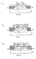
- Fig. 1 is a cross-sectional view of a semiconductor substrate having a silicon dioxide layer formed on its upper surface;
- Fig. 2 is a cross-sectional view of the structure shown in Fig. 1 after removal of a portion of the silicon dioxide layer;
- Fig. 3 is a further cross-sectional view showing a buried layer region formed in the surface of the semiconductor substrate;
- Fig. 4 is a further cross-sectional view after growing an epitaxial silicon layer;
- Fig. 5 is a further cross-sectional view after forming silicon nitride and silicon dioxide masking layers, etching the epitaxial silicon and doping the potential isolation oxide regions;
- Fig. 6 is a further cross-sectional view after forming isolation oxide regions;
- Fig. 7 is a further cross-sectional view after forming a thin oxide layer;
- Fig. 8 is a further cross-sectional view after .implanting first and second P- epitaxial regions;
- Fig. 9 is a further cross-sectional view after formation of an N+ polysilicon layer and an overlying silicon dioxide layer;
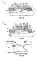
- Fig. 10 is a further cross-sectional view after forming first and second regions of N+ polysilicon;
- Fig. 11 is a further cross-sectional view after forming a silicon dioxide layer over the exposed surfaces of N+ silicon;
- Fig. 12 is a further cross-sectional view after formation of P+ regions in the epitaxial layer;
- Fig. 13 is a further cross-sectional view after forming a P+ polysilicon layer and an overlying layer of silicon dioxide;
- Fig. 14 is a cross-sectional view of the device which results from the process of the present invention;
- Fig. 15 is a circuit schematic for the structure shown in Fig. 14.
- Each step in the process of the present invention may be accomplished using known semiconductor technology. A preferred embodiment of the process is described in conjunction with Figs. 1-14.
- As shown in Fig. 1, a
wafer 10 comprising asubstrate 11 of P- type semiconductor material, with resistivity between 1.5 and 3.0 ohm centimeters and crystalline orientation 111 is thermally oxidized to create an overlyingsilicon dioxide layer 12. Thesubstrate 11 is oxidized by being subjected to 120 minutes of steam oxidation at 1000°C. These conditions produce asilicon dioxide layer 12 which is approximately 600-700 nm (6000-7000 Angstroms) thick. - Referring to Fig. 2, a layer of negative photoresist (not shown) is then formed across the upper surface of
silicon dioxide layer 12 and suitably patterned using well-known photolithographic techniques. The undesired portions oflayer 12 and all of the negative photoresist are then removed with an etching solution. In the preferred embodiment, thewafer 10 is exposed to the etching solution for 8-12 minutes. The etching solution comprises 15 milliliters of hydrofluoric acid (HF), 68 grams of ammonium fluoride (NH4F) and 100 milliliters of water (H20. After the etching is completed and the undesired portion oflayer 12 has been removed,regions - Next, as shown in Fig. 3, to form what will become a buried layer, a buried layer predeposi- tion step is performed in which the
wafer 10 is placed in an antimony atmosphere for 55 to 65 minutes to form an N+ buriedlayer region 13 in the upper surface ofsubstrate 11. Oxygen is then supplied to thewafer 10 for five minutes while the temperature of the structure is ramped to 1250°C. This creates a sheet resistivity for the N+ buriedlayer 13 of between 20 and 25 ohms per square.Silicon dioxide regions - As shown in Fig. 4, after removal of the
silicon dioxide regions layer 14 of epitaxial silicon is formed on the upper surface ofsubstrate 11 and buriedlayer 13. Using dichlorosilane, theepitaxial layer 14 will be formed between 1.35 and 1.55 micrometers thick with a resistivity of approximately 10 ohm centimeters. Phosphorus is then implanted into theepitaxial layer 14 to convert it to N- conductivity. Using well-known ion implantation techniques and an implant energy of 100,000 electron volts, an ion concentration of phosphorus of 2.5 x 10¹² ions/ cm2 is created in the epitaxial layer. This results in a sheet resistivity of approximately 4500 to 6800 ohms per square. - As shown in Fig. 5, a
layer 15 of silicon dioxide approximately 40-55 nm (400-550 Angstroms) thick is then formed on the upper surface of theepitaxial layer 14 by oxidizing thelayer 14 at 1000°C. Next, alayer 16 of silicon nitride (Si3N4) approximately 142.5-157.5 nm (1425-1575 Angstroms) thick is formed on the upper surface ofoxide layer 15 by any well-known technique, for example, vapor deposition. Then, athin layer 17 of silicon dioxide about 10 nm (100 Angstroms) thick is formed on the upper surface ofnitride layer 16 by exposing thenitride layer 16 to 1000°C steam oxidation for one hour. - The
oxide layer 17,nitride layer 16,oxide layer 15 andepitaxial layer 14 are then patterned to provide for what will become regions of isolation oxide. First, a layer of negative photoresist (not shown) is formed across the upper surface ofoxide layer 17. The photoresist is exposed and developed and serves as a mask for theoxide layer 17. Theoxide layer 17 is then etched using the same techniques discussed above. Next, thesilicon nitride layer 16 is etched using phosphoric acid (H2POS) for about one hour. Thewafer 10 is then dipped in hydrofluoric acid to remove theoxide layer 15. Then, approximately 520-560 nm (5200-5600 Angstroms) of theepitaxial layer 14 are removed using a silicon etch solution. One example of a suitable etch solution is a solution of one milliliter hydrofluoric acid, five milliliters HN03, and three milliliters of acedic acid. Next, as shown in Fig. 5, ion implantation is used to implant P+ conductivity type material, usually boron, intoregions 14a and 14b ofepitaxial layer 14. These regions may be formed using an implant energy of 20,000 electron volts to create a boron concentration of 1.2 x 10¹⁴ ion/cm2. - As shown in Fig. 6, the next step in the process is the formation of
regions wafer 10 at 1000°C for 170 minutes with pure nitrogen and then for . 10 hours with steam. The result will be silicon dioxide regions which are 1.3 to 1.7 micrometers thick and have a sheet resistivity of approximately 4000-6400 ohms per square. Theregions epitaxial layer 14 to the lateral junction between the buriedlayer 13 and thesubstrate 11 to form an electrically isolated pocket of N- epitaxial silicon. - In the above-described manner, a matrix of electrically isolated epitaxial pockets may be formed on the
wafer 10. - The oxide isolation process steps discussed above with respect to Figs. 1-6 are more fully described in U.S. patent no. 4,168,999 titled "Method for Forming Oxide isolated Integrated Injection Logic Semiconductor Structures Having Minimal Encroachment Utilizing Special Masking Techniques" issued to Vora et al.
- Additional information concerning oxide isolation techniques may be found in U.S. patent no. 3,648,125 titled "Method of Fabricating Integrated Circuits with Oxidized Isolation and the Resulting Structure" issued to Peltzer.
-
Oxide layer 17,nitride layer 16 andoxide layer 15 are then removed by well-known techniques. - According to the present invention and as shown in Fig. 7, a thin
silicon dioxide layer 19 about 20 nm (200 Angstroms) or less thick is then formed on the upper surface of the N-epitaxial pocket 14 and onoxide isolation regions layer 19. The exposed portions oflayer 19 are then removed using conventional etching techniques to form athin region 19a of oxide over theepitaxial pocket 14. Thethin oxide region 19a is formed such that first andsecond surface areas epitaxial pocket 14 are defined as shown in Fig. 8. - Next, as further shown in Fig. 8, the first and
second surface areas epitaxial regions epitaxial pocket 14. First and second P-regions thin oxide layer 19 is then removed by conventional techniques. - Next, as shown in Fig. 9, an N+ polysilicon layer 22 is formed on the exposed upper surface of the
wafer 10 by, for example, chemical vapor deposition. A layer 23 of silicon dioxide is then formed on the upper surface of the N+ polysilicon layer 22 by well-known techniques. A layer of negative photoresist (not shown) is then formed on the upper surface of silicon dioxide layer 23. The photoresist is used to selectively mask and pattern the silicon dioxide layer 23. - Then, as shown in Fig. 10, the N+ polysilicon layer 22 is etched to form a
first region 22a of N+ polysilicon on thethin oxide layer 19a and asecond region 22b of N+ polysilicon on the second P-region 21. For reasons which will be discussed below, thefirst region 22a of N+ polysilicon is formed on thethin oxide layer 19a such that edge portions of thethin oxide layer 19a are exposed as shown in Fig. 10. - The upper surface of a
wafer 10, including the exposed side surfaces of the first and secondN+ polysilicon regions wafer 10 in a manner such that N+ dopant fromregion 22b is driven into the underlying P-region 21 as shown in Fig. 12. Next, as shown in Fig. 11, the silicon dioxide layer is selectively patterned by plasma etch techniques to expose an upper surface 20a of the first P-region 20 and first and second selected portions 21 a and 21 b of the surface of the second P-region 21. Plasma etching of the silicon dioxide layer results in the definition of a secondsilicon dioxide region 24a which covers exposed surfaces of the firstN+ polysilicon region 22a and of a thirdsilicon dioxide region 24b which covers exposed surfaces of the secondN+ polysilicon region 22b as shown in Fig. 11. - Next, as shown in Fig. 12, the first upper surface area 20a and the first and second selected portions 21 a and 21 b are then subjected to ion implantation such that first, second and third
P+ epitaxial regions - Next, as shown in Fig. 13, a
layer 26 of P+ polysilicon is formed over the upper surface ofwafer 10 such that thelayer 26 contacts both the second and thirdP+ polysilicon regions P+ polysilicon layer 26.Polysilicon layer 26 andoxide layer 27 are then selectively patterned by forming a layer of negative photoresist (not shown) on the upper surface oflayer 27. As previously described, the photoresist is used to mask and pattern theoxide layer 27. - As shown in Fig. 14,
polysilicon layer 26 is then etched to form afirst region 26a of P+ polysilicon on thesilicon dioxide layer 24a which overlies thefirst region 22a of N+ polysilicon and asecond region 26b of P+ polysilicon on thesilicon dioxide layer 24b which overlies thesecond region 22b of N+ polysilicon. Thefirst region 26a of P+ polysilicon is formed on the edge portions of thethin oxide layer 19a such that it is electrically isolated from the underlying epitaxial pocket. The secondP+ polysilicon region 26b is defined such that it remains in contact with the second and third P+epitaxial regions - A layer of silicon dioxide is then formed over the surface of the
wafer 10, masked using photoresist as described above and etched to define fourth and fifthsilicon dioxide regions 28a and 28b which electrically isolate P+ polysilicon regions 16a and 16b, respectively. Alayer 29 of metal is then deposited over the surface of thewafer 10 and patterned using conventional techniques to produce the nonvolatile memory cell shown in Fig. 14. - The process of the present invention results in a high speed nonvolatile memory cell, the circuit schematic for which is shown in Fig. 15. The cell comprises a floating gate pMOS transistor for data storage and a merged npn bipolar transistor for selective access to stored data. The first N+ .
polysilicon region 22a forms the floating gate of the pMOS storage transistor which the firstP+ polysilicon region 26a formed its control gate. The second region ofN+ polysilicon 22b forms the emitter of the npn bipolar transistor. The second region ofP+ polysilicon 26b forms the contact to the second and third P+epitaxial regions layer 13 serves as the collector of the bipolar transistor.
Claims (6)
Applications Claiming Priority (2)
| Application Number | Priority Date | Filing Date | Title |
|---|---|---|---|
| US219784 | 1980-12-24 | ||
| US06/219,784 US4398338A (en) | 1980-12-24 | 1980-12-24 | Fabrication of high speed, nonvolatile, electrically erasable memory cell and system utilizing selective masking, deposition and etching techniques |
Related Child Applications (1)
| Application Number | Title | Priority Date | Filing Date |
|---|---|---|---|
| EP85112639.1 Division-Into | 1985-10-05 |
Publications (3)
| Publication Number | Publication Date |
|---|---|
| EP0055182A2 EP0055182A2 (en) | 1982-06-30 |
| EP0055182A3 EP0055182A3 (en) | 1983-06-22 |
| EP0055182B1 true EP0055182B1 (en) | 1986-10-22 |
Family
ID=22820767
Family Applications (2)
| Application Number | Title | Priority Date | Filing Date |
|---|---|---|---|
| EP85112639A Withdrawn EP0176111A1 (en) | 1980-12-24 | 1981-12-21 | High speed, nonvolatile, electrically erasable memory system |
| EP81402036A Expired EP0055182B1 (en) | 1980-12-24 | 1981-12-21 | High speed nonvolatile electrically erasable memory cell and system |
Family Applications Before (1)
| Application Number | Title | Priority Date | Filing Date |
|---|---|---|---|
| EP85112639A Withdrawn EP0176111A1 (en) | 1980-12-24 | 1981-12-21 | High speed, nonvolatile, electrically erasable memory system |
Country Status (4)
| Country | Link |
|---|---|
| US (1) | US4398338A (en) |
| EP (2) | EP0176111A1 (en) |
| JP (1) | JPS57172774A (en) |
| DE (1) | DE3175509D1 (en) |
Families Citing this family (21)
| Publication number | Priority date | Publication date | Assignee | Title |
|---|---|---|---|---|
| US4433470A (en) | 1981-05-19 | 1984-02-28 | Tokyo Shibaura Denki Kabushiki Kaisha | Method for manufacturing semiconductor device utilizing selective etching and diffusion |
| US4617071A (en) * | 1981-10-27 | 1986-10-14 | Fairchild Semiconductor Corporation | Method of fabricating electrically connected regions of opposite conductivity type in a semiconductor structure |
| US4488350A (en) * | 1981-10-27 | 1984-12-18 | Fairchild Camera & Instrument Corp. | Method of making an integrated circuit bipolar memory cell |
| US4622575A (en) * | 1981-10-27 | 1986-11-11 | Fairchild Semiconductor Corporation | Integrated circuit bipolar memory cell |
| US4507848A (en) * | 1982-11-22 | 1985-04-02 | Fairchild Camera & Instrument Corporation | Control of substrate injection in lateral bipolar transistors |
| US4527325A (en) * | 1983-12-23 | 1985-07-09 | International Business Machines Corporation | Process for fabricating semiconductor devices utilizing a protective film during high temperature annealing |
| US5243210A (en) * | 1987-02-21 | 1993-09-07 | Kabushiki Kaisha Toshiba | Semiconductor memory device and manufacturing method thereof |
| DE68916335T2 (en) * | 1988-08-08 | 1995-01-05 | Nat Semiconductor Corp | Electrically erasable and programmable read-only bipolar field effect memory cell and method for its production. |
| US5089433A (en) * | 1988-08-08 | 1992-02-18 | National Semiconductor Corporation | Bipolar field-effect electrically erasable programmable read only memory cell and method of manufacture |
| US5089429A (en) * | 1989-06-22 | 1992-02-18 | David Sarnoff Research Center, Inc. | Self-aligned emitter bicmos process |
| IT1237666B (en) * | 1989-10-31 | 1993-06-15 | Sgs Thomson Microelectronics | PROCESS FOR THE MANUFACTURE OF A PROGRAMMING VOLTAGE LIMITER COMPONENT AND BUILT-IN VOLTAGE STABILIZER IN AN ELECTRIC DEVICE WITH EEPROM MEMORY CELLS |
| JPH07123145B2 (en) * | 1990-06-27 | 1995-12-25 | 株式会社東芝 | Semiconductor integrated circuit |
| US5225700A (en) * | 1991-06-28 | 1993-07-06 | Texas Instruments Incorporated | Circuit and method for forming a non-volatile memory cell |
| US6534364B1 (en) * | 1994-12-05 | 2003-03-18 | Texas Instruments Incorporated | Tunnel diode layout for an EEPROM cell for protecting the tunnel diode region |
| US5576233A (en) * | 1995-06-21 | 1996-11-19 | Texas Instruments Incorporated | Method for making an EEPROM with thermal oxide isolated floating gate |
| US5747383A (en) * | 1995-09-05 | 1998-05-05 | Taiwan Semiconductor Manufacturing Company Ltd | Method for forming conductive lines and stacked vias |
| US5717635A (en) * | 1996-08-27 | 1998-02-10 | International Business Machines Corporation | High density EEPROM for solid state file |
| US6060360A (en) * | 1997-04-14 | 2000-05-09 | Taiwan Semiconductor Manufacturing Company | Method of manufacture of P-channel EEprom and flash EEprom devices |
| US7745301B2 (en) | 2005-08-22 | 2010-06-29 | Terapede, Llc | Methods and apparatus for high-density chip connectivity |
| US8957511B2 (en) | 2005-08-22 | 2015-02-17 | Madhukar B. Vora | Apparatus and methods for high-density chip connectivity |
| US8320191B2 (en) | 2007-08-30 | 2012-11-27 | Infineon Technologies Ag | Memory cell arrangement, method for controlling a memory cell, memory array and electronic device |
Family Cites Families (11)
| Publication number | Priority date | Publication date | Assignee | Title |
|---|---|---|---|---|
| US3609479A (en) * | 1968-02-29 | 1971-09-28 | Westinghouse Electric Corp | Semiconductor integrated circuit having mis and bipolar transistor elements |
| US3648125A (en) * | 1971-02-02 | 1972-03-07 | Fairchild Camera Instr Co | Method of fabricating integrated circuits with oxidized isolation and the resulting structure |
| US3893085A (en) * | 1973-11-28 | 1975-07-01 | Ibm | Read mostly memory cell having bipolar and FAMOS transistor |
| US3996657A (en) * | 1974-12-30 | 1976-12-14 | Intel Corporation | Double polycrystalline silicon gate memory device |
| GB1480201A (en) * | 1975-01-06 | 1977-07-20 | Ncr Co | Four zone semiconductor device |
| US4258378A (en) * | 1978-05-26 | 1981-03-24 | Texas Instruments Incorporated | Electrically alterable floating gate memory with self-aligned low-threshold series enhancement transistor |
| US4234362A (en) * | 1978-11-03 | 1980-11-18 | International Business Machines Corporation | Method for forming an insulator between layers of conductive material |
| US4168999A (en) * | 1978-12-26 | 1979-09-25 | Fairchild Camera And Instrument Corporation | Method for forming oxide isolated integrated injection logic semiconductor structures having minimal encroachment utilizing special masking techniques |
| US4247861A (en) * | 1979-03-09 | 1981-01-27 | Rca Corporation | High performance electrically alterable read-only memory (EAROM) |
| US4237472A (en) * | 1979-03-12 | 1980-12-02 | Rca Corporation | High performance electrically alterable read only memory (EAROM) |
| US4322883A (en) * | 1980-07-08 | 1982-04-06 | International Business Machines Corporation | Self-aligned metal process for integrated injection logic integrated circuits |
-
1980
- 1980-12-24 US US06/219,784 patent/US4398338A/en not_active Expired - Lifetime
-
1981
- 1981-12-21 DE DE8181402036T patent/DE3175509D1/en not_active Expired
- 1981-12-21 EP EP85112639A patent/EP0176111A1/en not_active Withdrawn
- 1981-12-21 EP EP81402036A patent/EP0055182B1/en not_active Expired
- 1981-12-24 JP JP20827181A patent/JPS57172774A/en active Pending
Also Published As
| Publication number | Publication date |
|---|---|
| EP0055182A2 (en) | 1982-06-30 |
| EP0055182A3 (en) | 1983-06-22 |
| DE3175509D1 (en) | 1986-11-27 |
| JPS57172774A (en) | 1982-10-23 |
| US4398338A (en) | 1983-08-16 |
| EP0176111A1 (en) | 1986-04-02 |
Similar Documents
| Publication | Publication Date | Title |
|---|---|---|
| US4398338A (en) | Fabrication of high speed, nonvolatile, electrically erasable memory cell and system utilizing selective masking, deposition and etching techniques | |
| US4822750A (en) | MOS floating gate memory cell containing tunneling diffusion region in contact with drain and extending under edges of field oxide | |
| US4701776A (en) | MOS floating gate memory cell and process for fabricating same | |
| US4078947A (en) | Method for forming a narrow channel length MOS field effect transistor | |
| EP0442144B1 (en) | Manufacturing high speed low leakage radiation hardened CMOS/SOI devices | |
| EP0039411B1 (en) | Process for fabricating an integrated pnp and npn transistor structure | |
| EP0164605B1 (en) | Method of manufacturing nonvolatile semiconductor eeprom device | |
| US4498227A (en) | Wafer fabrication by implanting through protective layer | |
| US4435790A (en) | High speed, nonvolatile, electrically erasable memory cell and system | |
| US4168999A (en) | Method for forming oxide isolated integrated injection logic semiconductor structures having minimal encroachment utilizing special masking techniques | |
| US4874714A (en) | Method of making laterally oriented Schottky diode | |
| EP0123726B1 (en) | Method for fabricating deis structure between two polysilicon gate electrodes and memories resulting therefrom | |
| US5089433A (en) | Bipolar field-effect electrically erasable programmable read only memory cell and method of manufacture | |
| JPS62203380A (en) | Semiconductor device and manufacture of the same | |
| US4443933A (en) | Utilizing multi-layer mask to define isolation and device zones in a semiconductor substrate | |
| EP0160003B1 (en) | Mos floating gate memory cell and process for fabricating same | |
| JPH0361337B2 (en) | ||
| JPS6273655A (en) | Highly planar integrated circuit structure | |
| GB1587398A (en) | Semiconductor device manufacture | |
| EP0058124B1 (en) | Polycrystalline silicon schottky diode array and method of manufacturing | |
| EP0386798A2 (en) | A method for forming a channel stopper in a semiconductor structure | |
| GB2080024A (en) | Semiconductor Device and Method for Fabricating the Same | |
| JPS59204232A (en) | Method of forming ion implanted region | |
| CA1327646C (en) | Bipolar field-effect electrically erasable programmable read only memory cell and method of manufacture | |
| EP0743682A2 (en) | Integrated injection logic semiconductor device and method of fabricating the same |
Legal Events
| Date | Code | Title | Description |
|---|---|---|---|
| PUAI | Public reference made under article 153(3) epc to a published international application that has entered the european phase |
Free format text: ORIGINAL CODE: 0009012 |
|
| AK | Designated contracting states |
Designated state(s): DE FR GB IT NL |
|
| PUAL | Search report despatched |
Free format text: ORIGINAL CODE: 0009013 |
|
| AK | Designated contracting states |
Designated state(s): DE FR GB IT NL |
|
| 17P | Request for examination filed |
Effective date: 19831220 |
|
| GRAA | (expected) grant |
Free format text: ORIGINAL CODE: 0009210 |
|
| ITF | It: translation for a ep patent filed | ||
| AK | Designated contracting states |
Kind code of ref document: B1 Designated state(s): DE FR GB IT NL |
|
| REF | Corresponds to: |
Ref document number: 3175509 Country of ref document: DE Date of ref document: 19861127 |
|
| ET | Fr: translation filed | ||
| PLBE | No opposition filed within time limit |
Free format text: ORIGINAL CODE: 0009261 |
|
| STAA | Information on the status of an ep patent application or granted ep patent |
Free format text: STATUS: NO OPPOSITION FILED WITHIN TIME LIMIT |
|
| 26N | No opposition filed | ||
| ITTA | It: last paid annual fee | ||
| PGFP | Annual fee paid to national office [announced via postgrant information from national office to epo] |
Ref country code: GB Payment date: 19941111 Year of fee payment: 14 |
|
| PGFP | Annual fee paid to national office [announced via postgrant information from national office to epo] |
Ref country code: FR Payment date: 19941209 Year of fee payment: 14 |
|
| PGFP | Annual fee paid to national office [announced via postgrant information from national office to epo] |
Ref country code: NL Payment date: 19941231 Year of fee payment: 14 |
|
| PG25 | Lapsed in a contracting state [announced via postgrant information from national office to epo] |
Ref country code: GB Effective date: 19951221 |
|
| PG25 | Lapsed in a contracting state [announced via postgrant information from national office to epo] |
Ref country code: NL Effective date: 19960701 |
|
| GBPC | Gb: european patent ceased through non-payment of renewal fee |
Effective date: 19951221 |
|
| PG25 | Lapsed in a contracting state [announced via postgrant information from national office to epo] |
Ref country code: FR Effective date: 19960830 |
|
| NLV4 | Nl: lapsed or anulled due to non-payment of the annual fee |
Effective date: 19960701 |
|
| REG | Reference to a national code |
Ref country code: FR Ref legal event code: ST |
|
| PGFP | Annual fee paid to national office [announced via postgrant information from national office to epo] |
Ref country code: DE Payment date: 20001211 Year of fee payment: 20 |