EP0055098B1 - Video signal recording-reproducing apparatus - Google Patents
Video signal recording-reproducing apparatus Download PDFInfo
- Publication number
- EP0055098B1 EP0055098B1 EP81305956A EP81305956A EP0055098B1 EP 0055098 B1 EP0055098 B1 EP 0055098B1 EP 81305956 A EP81305956 A EP 81305956A EP 81305956 A EP81305956 A EP 81305956A EP 0055098 B1 EP0055098 B1 EP 0055098B1
- Authority
- EP
- European Patent Office
- Prior art keywords
- signal
- frequency
- carrier wave
- recording
- signals
- Prior art date
- Legal status (The legal status is an assumption and is not a legal conclusion. Google has not performed a legal analysis and makes no representation as to the accuracy of the status listed.)
- Expired
Links
Images


Classifications
-
- H—ELECTRICITY
- H04—ELECTRIC COMMUNICATION TECHNIQUE
- H04N—PICTORIAL COMMUNICATION, e.g. TELEVISION
- H04N9/00—Details of colour television systems
- H04N9/79—Processing of colour television signals in connection with recording
- H04N9/80—Transformation of the television signal for recording, e.g. modulation, frequency changing; Inverse transformation for playback
- H04N9/82—Transformation of the television signal for recording, e.g. modulation, frequency changing; Inverse transformation for playback the individual colour picture signal components being recorded simultaneously only
- H04N9/825—Transformation of the television signal for recording, e.g. modulation, frequency changing; Inverse transformation for playback the individual colour picture signal components being recorded simultaneously only the luminance and chrominance signals being recorded in separate channels
Definitions
- This invention relates to a video signal recording-reproducing apparatus having a small size and light weight, capable of generating a high quality reproduction signal, or more particularly, reproducing color or chrominance signals with unnecessary components largely reduced.
- VTR magnetic video tape recorders
- the main stream of magnetic video tape recorders lie in the helical scan system using rotating heads.
- VTR for broadcasting it is described that the portable VTR for ELECTRONIC NEWS GATHERING (ENG) be small in size and light in weight.
- the VTR of 4 inch U standard is now remarkably progressing.
- the VTR for ENG is required not only to be small and light but also to have a high quality because it is used for TV broadcasting. Since the VTR of inch U standard, however, has a cylinder diameter of 110 mm and a tape width of inch, there is a limit to its miniaturization. In these video signal recording systems, the luminance signal is frequency-molulated with its low frequency band eliminated and a carrier chrominance signal converted into a lower frequency band is superimposed on it.
- the frequency bands of the luminance and the chrominance signals are restricted, and the video quality is not always suited to broadcasting purposes.
- EP-A-0038670 (Published 28.10.81) describes a portable VTR which is small in size, light in weight and capable of providing high video quality.
- the luminance and chrominance signals are separately recorded on, and reproduced from respective tracks during recording, a carrier wave of a first frequency and a carrier wave of a second frequency are frequency modulated by two signal components to constitute an image signal and these modulated signals are superimposed on each other and recorded in a recording medium.
- the modulated carrier wave of the first frequency is frequency-converted by a third carrier wave of a higher frequency before it is demodulated. According to such a technique, the bandwidth of both the luminance and chrominance signals can be more greatly expanded than with other prior art methods.
- the present invention employs the above-mentioned technique and is characterised by means for selecting the frequency of the third carrier wave so that it is separated from the sum of the frequencies of the first and second carrier waves by more than the frequency bandwidth of the demodulated signal of the third carrier wave.
- the invention enables the production of small and light apparatus capable of reproducing a video signal of high quality. For example, even with a cylinder diameter and cassette as large as those of a VTR in a VHS system, a high quality video signal can be obtained. Moreover, the size and weight can be made smaller than those of prior art VTR for ENG.
- DE-A-1437306 discloses the recording and reproducing of luminance and chrominance signals on respective tracks by respective heads and US-A-4188638 discloses the recording and reproducing of such signals in a superposed mode.
- Fig. 1 (which is based on Fig. 4 of EP-A-0038670) shows a block diagram of a circuit for recording and reproducing luminance and chrominance signals in separate tracks.
- a reference numeral 1 denotes an input terminal for the luminance signal (Y signal); 2 is an input terminal for the I signal; 3 is an input terminal for the Q signal; 4, 5 and 6 are frequency modulators; 7 is a band pass filter; 8 is a low pass filter; 9 is an adder; 10 and 11 are recording amplifiers; 12 and 13 are video heads; 14 and 15 are reproducing amplifiers; 17 is a band pass filter; 18 is a low pass filter; 16, 21 and 22 are amplitude limiters; 19, 20 and 23 are frequency demodulators; 24 is an output terminal for the Y signal; 25 is an output terminal for the I signal; and 26 is an output terminal for the Q signal.
- the Y signal is applied to the input terminal 1 and modulated by the frequency modulator 4. After the signal is amplified by the recording amplifier 10, it is recorded in a tape through the head 12.
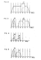
- the spectrum of the frequency modulated Y signal is as shown by 27 in Fig. 2.
- the I signal applied to the input terminal 2 is modulated by the frequency modulator 5, bandlimited about from 3 MHz to 8 MHz by the band pass filter 7, and introduced into the adder 9.
- the Q signal applied to the input terminal 3 is modulated by the frequency modulator 6, bandlimited in or not higher than about 2 MHz by the low pass filter 8, and introduced into the adder 9.
- the band pass filter 7 and the low pass filter 8 limits the band of the I and Q signals, respectively, such that the spectra of these frequency modulated waves are not superimposed on each other.
- the two signals added by the adder 9 are amplified by the recording amplifier 11 and then recorded onto a tape by the head 13.
- the opposite frequency deviation of the I signal is about 5 to 6 MHz, while that of the Q signal is about 0.75 to 1.25 MHz.
- the record spectra of the chrominance signals I and Q are as shown by 28 and 29 in Fig. 3, respectively.
- the Y signal and the chrominance signals are recorded by two pairs of heads.
- the Y signal picked up by the head 12 is amplified by the reproducing amplifier 14, passed through the amplitude limiter 16, and demodulated by the frequency demodulator 19.
- the Y signal appears reproduced at the output terminal 24.
- the chrominance signal picked up by the head 13 is amplified by the reproducing amplifier 15 and introduced into the band pass filter 17 and the low pass filter 18, the I signal passes the former while the Q signal passes the latter.
- the amplitudes of both signals are limited by amplitude limiters 21 and 22. After demodulation by frequency demodulators 20 and 23, 1 and Q signals appear reproduced at the output terminals 25 and 26, respectively.
- An essential point of this invention is to locate the third harmonic waves generated by the limiters and unnecessary components generated by the frequency converters, out of the frequency band of the Q signal by means of converting the frequency of the reproduced Q signal into a high frequency band before the signal is demodulated and to set, for the purpose, a carrier wave frequency f 3 to which the Q signal frequency is converted in the high frequency conversion.
- a reference numeral 43 denotes an input terminal for the output signal of the low pass filter of Fig. 1; 44 is a frequency converter; 45 is an oscillator; 46 is a limiter; 47 is a frequency demodulator; 48 is a low pass filter; and 49 is an output terminal for the demodulated Q signal.
- the frequency f 3 of the Q signal (29 in Fig. 3) applied to the terminal 43 is converted to f G + f o by the oscillator 45 (oscillating at a frequency f G ) and the frequency converter 44. If f G is chosen to exceed a certain value, beats between the noise of the converter output signal and that of the third harmonic wave and beats between the side bands of the converter output signal and those of the third harmonic wave do not appear even after the converter output signal is made to pass through the limiter 46. In this manner, by converting the Q signal into a high frequency region, demodulating it by the frequency demodulator 47 and passing it through the low pass filter 48, the reproduced signal has few unnecessary components and is of good quality.
- the frequency converter has a nonlinear element. If the I signal is cut off too sharply by the low pass filter 18, distortion of the wave becomes large. Therefore, the characteristic of the low pass filter may not be made so sharp.
- the filter output includes the I signal mixed with the Q signal.
- the input signal to the frequency converter 44 contains the I signal as well as the Q signal. If the value of f G is simply chosen in such a manner that the noise or side band of the signal may not be overlapped with that of the higher harmonic component, an influence of the unnecessary components, still appears.
- the conversion frequency f G should be selected as follows.
- the output of the low pass filter 18 of Fig. 1 contains I signal.
- the output of the frequency converter 44 contains components of f, + f o (sum frequency of I and Q signals), f, - f o (difference frequency of I and Q signals), and f, (I signal) other than the components of f G ⁇ f Q -and f G .
- a reference numeral 36 denotes the component of f G + f a and 37, 38, 39, 40, 41 and 42 denote components of f G - f Q , f Q , f l , ⁇ f Q , f l , f, + f Q and f G , respectively.
- the frequency f, + f Q is nearest to the high frequency converted one, f G + f Q . Therefore, if f G is selected such that the component of f, + f a is apart from that of f G + f Q by more than f QW (band width of the demodulation signal of Q), no harmful effect would appear.
- the frequency f Q of the first carrier wave is converted by f G , the frequency f 3 of the third carrier wave becomes If this third carrier wave frequency is set as any harmful effect or interference will be suppressed.
- the frequency deviation of the Q signal is 0.75 to 1.25 MHz, that of the I signal is 5 to 6 MHz and that the demodulation signal band width f QW of the Q signal is 0.5 MHz; we obtain from (1) where the value if f, is assumed to be 6 MHz, i.e., the upper limit of the frequency deviation.
- a reference numeral 50 denotes f G - f a , 51: f G + f Q , 52: f Q , 53: f, - f a , 54: f l , 55: f, + f a , and 56: f G .
- the frequency f 3 of the third carrier wave is given by (from the equation (2))
- the Q signal modulated by the third carrier wave is no longer affected by the third harmonic wave due to the limiters, nor by a leakage of the I signal.
Description
- This invention relates to a video signal recording-reproducing apparatus having a small size and light weight, capable of generating a high quality reproduction signal, or more particularly, reproducing color or chrominance signals with unnecessary components largely reduced.
- The main stream of magnetic video tape recorders (hereinafter referred to as VTR) at present lie in the helical scan system using rotating heads. For example, in a VTR of VHS system, the video signal is recorded slantingly with respect to a 2 inch (1 inch = 25.4 mm) wide tape by using two video heads which are disposed on a rotating cylinder of 62 mm diameter with 180° angularly- displaced positional relation. In the case of VTR for broadcasting, it is described that the portable VTR for ELECTRONIC NEWS GATHERING (ENG) be small in size and light in weight. The VTR of 4 inch U standard is now remarkably progressing. The VTR for ENG is required not only to be small and light but also to have a high quality because it is used for TV broadcasting. Since the VTR of inch U standard, however, has a cylinder diameter of 110 mm and a tape width of inch, there is a limit to its miniaturization. In these video signal recording systems, the luminance signal is frequency-molulated with its low frequency band eliminated and a carrier chrominance signal converted into a lower frequency band is superimposed on it.
- Therefore, the frequency bands of the luminance and the chrominance signals are restricted, and the video quality is not always suited to broadcasting purposes.
- EP-A-0038670 (Published 28.10.81) describes a portable VTR which is small in size, light in weight and capable of providing high video quality. In the latter VTR, the luminance and chrominance signals are separately recorded on, and reproduced from respective tracks during recording, a carrier wave of a first frequency and a carrier wave of a second frequency are frequency modulated by two signal components to constitute an image signal and these modulated signals are superimposed on each other and recorded in a recording medium. During reproduction, the modulated carrier wave of the first frequency is frequency-converted by a third carrier wave of a higher frequency before it is demodulated. According to such a technique, the bandwidth of both the luminance and chrominance signals can be more greatly expanded than with other prior art methods.
- The present invention employs the above-mentioned technique and is characterised by means for selecting the frequency of the third carrier wave so that it is separated from the sum of the frequencies of the first and second carrier waves by more than the frequency bandwidth of the demodulated signal of the third carrier wave.
- The invention enables the production of small and light apparatus capable of reproducing a video signal of high quality. For example, even with a cylinder diameter and cassette as large as those of a VTR in a VHS system, a high quality video signal can be obtained. Moreover, the size and weight can be made smaller than those of prior art VTR for ENG.
- DE-A-1437306 discloses the recording and reproducing of luminance and chrominance signals on respective tracks by respective heads and US-A-4188638 discloses the recording and reproducing of such signals in a superposed mode.
- An embodiment of the invention will be described with reference to Fig. 7 of the accompanying drawings, in which drawings:
- Fig. 1 is a block diagram of the circuit of a magnetic video recording and reproducing apparatus which records and reproduces the luminance and chrominance signal by different heads;
- Fig. 2 shows a spectrum of a Y signal modulated by a frequency converter of Fig. 1;
- Fig. 3 shows a spectrum of I and Q signals modulated by a respective frequency modulator of Fig. 1;
- Fig. 4 shows spectra of the noise of the Q signal and the noise of the third harmonic wave of the Q signal;
- Fig. 5 shows a spectra of the frequency modulated Q signal and its third harmonic wave;
- Fig. 6 shows a spectrum of the output of the frequency converter where the carrier wave of a reproduced chrominance signal is converted to a high frequency wave;
- Fig. 7 is a block diagram showing the main part of one embodiment of this invention; and
- Fig. 8 shows a spectrum of the output of a
frequency converter 44 of the embodiment of Fig. 7. - Fig. 1 (which is based on Fig. 4 of EP-A-0038670) shows a block diagram of a circuit for recording and reproducing luminance and chrominance signals in separate tracks. A
reference numeral 1 denotes an input terminal for the luminance signal (Y signal); 2 is an input terminal for the I signal; 3 is an input terminal for the Q signal; 4, 5 and 6 are frequency modulators; 7 is a band pass filter; 8 is a low pass filter; 9 is an adder; 10 and 11 are recording amplifiers; 12 and 13 are video heads; 14 and 15 are reproducing amplifiers; 17 is a band pass filter; 18 is a low pass filter; 16, 21 and 22 are amplitude limiters; 19, 20 and 23 are frequency demodulators; 24 is an output terminal for the Y signal; 25 is an output terminal for the I signal; and 26 is an output terminal for the Q signal. - In Fig. 1, the Y signal is applied to the
input terminal 1 and modulated by thefrequency modulator 4. After the signal is amplified by therecording amplifier 10, it is recorded in a tape through thehead 12. The spectrum of the frequency modulated Y signal is as shown by 27 in Fig. 2. The I signal applied to theinput terminal 2 is modulated by thefrequency modulator 5, bandlimited about from 3 MHz to 8 MHz by theband pass filter 7, and introduced into theadder 9. The Q signal applied to theinput terminal 3 is modulated by thefrequency modulator 6, bandlimited in or not higher than about 2 MHz by thelow pass filter 8, and introduced into theadder 9. Theband pass filter 7 and thelow pass filter 8 limits the band of the I and Q signals, respectively, such that the spectra of these frequency modulated waves are not superimposed on each other. The two signals added by theadder 9 are amplified by the recording amplifier 11 and then recorded onto a tape by thehead 13. The opposite frequency deviation of the I signal is about 5 to 6 MHz, while that of the Q signal is about 0.75 to 1.25 MHz. The record spectra of the chrominance signals I and Q are as shown by 28 and 29 in Fig. 3, respectively. - The Y signal and the chrominance signals (I signal and Q signal) are recorded by two pairs of heads. In the reproduction process, the Y signal picked up by the
head 12 is amplified by the reproducingamplifier 14, passed through theamplitude limiter 16, and demodulated by thefrequency demodulator 19. As a result, the Y signal appears reproduced at the output terminal 24. The chrominance signal picked up by thehead 13 is amplified by the reproducingamplifier 15 and introduced into theband pass filter 17 and thelow pass filter 18, the I signal passes the former while the Q signal passes the latter. The amplitudes of both signals are limited byamplitude limiters frequency demodulators output terminals 25 and 26, respectively. - In the demodulation process, since I and Q signals are made to pass through amplitude limiters (hereinafter referred to as limiters) to remove any amplitude variation, third harmonic waves appear, the level of which is lower than that of the fundamental waves by about 10 dB. Furthermore, the reproduced signals contain noise. If the signal frequency is low, noise components of the third harmonic wave enter within the band width of the fundamentals and generate beat waves through an interaction with the noise of the fundamentals. Fig. 4 shows spectra of the reproduced
Q signal 30 at one frequency and thenoise 31 thereof, and spectra of the thirdharmonic wave 32 and the noise thereof 33 that are generated by the limiter. The same effect as caused by the noise happens also between side bands of each signal. Namely, as can be understood from Fig. 5, the side bands of thefundamental wave 34 overlap with those of the thirdharmonic wave 35, thereby generating beat waves. This invention aims at removing these shortcomings. One embodiment of this invention will be explained next with reference to Figures. - An essential point of this invention is to locate the third harmonic waves generated by the limiters and unnecessary components generated by the frequency converters, out of the frequency band of the Q signal by means of converting the frequency of the reproduced Q signal into a high frequency band before the signal is demodulated and to set, for the purpose, a carrier wave frequency f3 to which the Q signal frequency is converted in the high frequency conversion.
- A circuit construction for eliminating the beats between the noise of the fundamental waves and that of the third harmonic waves as well as the beats between the side bands of the fundamental wave and those of the third harmonic wave will be explained next in conjunction with Fig. 7. In this Figure, a
reference numeral 43 denotes an input terminal for the output signal of the low pass filter of Fig. 1; 44 is a frequency converter; 45 is an oscillator; 46 is a limiter; 47 is a frequency demodulator; 48 is a low pass filter; and 49 is an output terminal for the demodulated Q signal. - The frequency f3 of the Q signal (29 in Fig. 3) applied to the
terminal 43 is converted to fG + fo by the oscillator 45 (oscillating at a frequency fG) and thefrequency converter 44. If fG is chosen to exceed a certain value, beats between the noise of the converter output signal and that of the third harmonic wave and beats between the side bands of the converter output signal and those of the third harmonic wave do not appear even after the converter output signal is made to pass through thelimiter 46. In this manner, by converting the Q signal into a high frequency region, demodulating it by thefrequency demodulator 47 and passing it through thelow pass filter 48, the reproduced signal has few unnecessary components and is of good quality. - However, the frequency converter has a nonlinear element. If the I signal is cut off too sharply by the
low pass filter 18, distortion of the wave becomes large. Therefore, the characteristic of the low pass filter may not be made so sharp. - After the passage of the low pass filter, the filter output includes the I signal mixed with the Q signal. Namely the input signal to the
frequency converter 44 contains the I signal as well as the Q signal. If the value of fG is simply chosen in such a manner that the noise or side band of the signal may not be overlapped with that of the higher harmonic component, an influence of the unnecessary components, still appears. - Therefore, the conversion frequency fG should be selected as follows.
- The output of the
low pass filter 18 of Fig. 1 contains I signal. The output of thefrequency converter 44 contains components of f, + fo (sum frequency of I and Q signals), f, - fo (difference frequency of I and Q signals), and f, (I signal) other than the components of fG ± fQ -and fG. The output of thefrequency converter 44 for the case of f, = 5.5 MHz, fo = 1.0 MHz and fG = 6 MHz is shown in Fig. 6. Areference numeral 36 denotes the component of fG + fa and 37, 38, 39, 40, 41 and 42 denote components of f G - fQ, fQ, fl, ― fQ, fl, f, + fQ and fG, respectively. Here, the frequency f, + fQ is nearest to the high frequency converted one, fG + fQ. Therefore, if fG is selected such that the component of f, + fa is apart from that of fG + fQ by more than fQW (band width of the demodulation signal of Q), no harmful effect would appear. - Hence, the following relation should be satisfied.


reference numeral 50 denotes fG - fa, 51: fG + fQ, 52: fQ, 53: f, - fa, 54: fl, 55: f, + fa, and 56: fG. As can be seen from the Figure, unnecessary components are separated from the component of fG + fQ by more than fQW (= 0.5 MHz). The frequency f3 of the third carrier wave is given by (from the equation (2))
Claims (3)
Applications Claiming Priority (2)
| Application Number | Priority Date | Filing Date | Title |
|---|---|---|---|
| JP55180683A JPS57104392A (en) | 1980-12-19 | 1980-12-19 | Video signal recording and reproducing device |
| JP180683/80 | 1980-12-19 |
Publications (3)
| Publication Number | Publication Date |
|---|---|
| EP0055098A2 EP0055098A2 (en) | 1982-06-30 |
| EP0055098A3 EP0055098A3 (en) | 1984-01-11 |
| EP0055098B1 true EP0055098B1 (en) | 1986-10-01 |
Family
ID=16087473
Family Applications (1)
| Application Number | Title | Priority Date | Filing Date |
|---|---|---|---|
| EP81305956A Expired EP0055098B1 (en) | 1980-12-19 | 1981-12-18 | Video signal recording-reproducing apparatus |
Country Status (4)
| Country | Link |
|---|---|
| US (1) | US4477837A (en) |
| EP (1) | EP0055098B1 (en) |
| JP (1) | JPS57104392A (en) |
| DE (1) | DE3175432D1 (en) |
Families Citing this family (3)
| Publication number | Priority date | Publication date | Assignee | Title |
|---|---|---|---|---|
| EP0374128A3 (en) * | 1982-07-07 | 1990-09-12 | Rai Radiotelevisione Italiana | Method of transmitting and receiving color television signals on two channels for broadcasting from satellite and apparatus for carrying out said method |
| DE3481262D1 (en) * | 1983-09-30 | 1990-03-08 | Victor Company Of Japan | METHOD AND DEVICE FOR RECORDING AND / OR PLAYING BACK COLOR VIDEO SIGNALS. |
| US5067026A (en) * | 1988-05-06 | 1991-11-19 | Sony Corporation | Apparatus for recording and reproducing a video signal |
Family Cites Families (3)
| Publication number | Priority date | Publication date | Assignee | Title |
|---|---|---|---|---|
| US4045812A (en) * | 1974-02-13 | 1977-08-30 | U.S. Philips Corporation | Color television recording system employing frequency modulation and pulse width modulation |
| US4188638A (en) * | 1975-04-22 | 1980-02-12 | U.S. Philips Corporation | Color television signal having color-difference signals alternating between two carriers |
| JPS56144690A (en) * | 1980-04-14 | 1981-11-11 | Matsushita Electric Ind Co Ltd | Recording system for video signal |
-
1980
- 1980-12-19 JP JP55180683A patent/JPS57104392A/en active Pending
-
1981
- 1981-12-16 US US06/331,276 patent/US4477837A/en not_active Expired - Lifetime
- 1981-12-18 DE DE8181305956T patent/DE3175432D1/en not_active Expired
- 1981-12-18 EP EP81305956A patent/EP0055098B1/en not_active Expired
Also Published As
| Publication number | Publication date |
|---|---|
| JPS57104392A (en) | 1982-06-29 |
| EP0055098A3 (en) | 1984-01-11 |
| DE3175432D1 (en) | 1986-11-06 |
| EP0055098A2 (en) | 1982-06-30 |
| US4477837A (en) | 1984-10-16 |
Similar Documents
| Publication | Publication Date | Title |
|---|---|---|
| CA1182904A (en) | Videorecorder for recording a vision carrier that is frequency modulated with a video signal | |
| US4425585A (en) | Video tape recorder immune to third-order distortion noise | |
| KR920003521B1 (en) | Magnetic recording/reproducing device | |
| EP0055098B1 (en) | Video signal recording-reproducing apparatus | |
| EP0177235B1 (en) | Apparatus for recording audio and video signals | |
| JP2748464B2 (en) | Magnetic recording device | |
| JPS6214906B2 (en) | ||
| JPS5880990A (en) | Recording and reproducing device for color television signal | |
| JPS62226791A (en) | Video recorder with high quality acoustic recording | |
| JPS63217781A (en) | Video signal recording method | |
| JPS5851474B2 (en) | Color television signal recording method | |
| JPS5836876B2 (en) | SECAM color video signal recording and playback system | |
| JP2627967B2 (en) | Video tape recorder | |
| KR950002760Y1 (en) | Frequency transformation system of vcr | |
| JP2635846B2 (en) | Magnetic recording device | |
| JP2625051B2 (en) | Magnetic playback device | |
| JPH0442750B2 (en) | ||
| JPH0722372B2 (en) | Modulation circuit of magnetic recording / reproducing apparatus | |
| JPS5847914B2 (en) | SECAM color video signal recording and playback system | |
| JPS5940308A (en) | Modulating system of video disk recorder | |
| JPH0468830B2 (en) | ||
| JPS63209003A (en) | Magnetic recording method | |
| JPH05153619A (en) | Magnetic recorder | |
| JPS625785A (en) | Sound signal recording and reproducing device | |
| JPH04271684A (en) | Correcting circuit for magnetic recording |
Legal Events
| Date | Code | Title | Description |
|---|---|---|---|
| PUAI | Public reference made under article 153(3) epc to a published international application that has entered the european phase |
Free format text: ORIGINAL CODE: 0009012 |
|
| AK | Designated contracting states |
Designated state(s): DE FR GB |
|
| PUAL | Search report despatched |
Free format text: ORIGINAL CODE: 0009013 |
|
| AK | Designated contracting states |
Designated state(s): DE FR GB |
|
| 17P | Request for examination filed |
Effective date: 19840531 |
|
| GRAA | (expected) grant |
Free format text: ORIGINAL CODE: 0009210 |
|
| AK | Designated contracting states |
Kind code of ref document: B1 Designated state(s): DE FR GB |
|
| REF | Corresponds to: |
Ref document number: 3175432 Country of ref document: DE Date of ref document: 19861106 |
|
| ET | Fr: translation filed | ||
| PLBE | No opposition filed within time limit |
Free format text: ORIGINAL CODE: 0009261 |
|
| STAA | Information on the status of an ep patent application or granted ep patent |
Free format text: STATUS: NO OPPOSITION FILED WITHIN TIME LIMIT |
|
| 26N | No opposition filed | ||
| PGFP | Annual fee paid to national office [announced via postgrant information from national office to epo] |
Ref country code: GB Payment date: 19941208 Year of fee payment: 14 Ref country code: DE Payment date: 19941208 Year of fee payment: 14 |
|
| PGFP | Annual fee paid to national office [announced via postgrant information from national office to epo] |
Ref country code: FR Payment date: 19941209 Year of fee payment: 14 |
|
| PG25 | Lapsed in a contracting state [announced via postgrant information from national office to epo] |
Ref country code: GB Effective date: 19951218 |
|
| GBPC | Gb: european patent ceased through non-payment of renewal fee |
Effective date: 19951218 |
|
| PG25 | Lapsed in a contracting state [announced via postgrant information from national office to epo] |
Ref country code: FR Effective date: 19960830 |
|
| PG25 | Lapsed in a contracting state [announced via postgrant information from national office to epo] |
Ref country code: DE Effective date: 19960903 |
|
| REG | Reference to a national code |
Ref country code: FR Ref legal event code: ST |