EP0054888B1 - Data-processing system with main and buffer storage control - Google Patents
Data-processing system with main and buffer storage control Download PDFInfo
- Publication number
- EP0054888B1 EP0054888B1 EP81110452A EP81110452A EP0054888B1 EP 0054888 B1 EP0054888 B1 EP 0054888B1 EP 81110452 A EP81110452 A EP 81110452A EP 81110452 A EP81110452 A EP 81110452A EP 0054888 B1 EP0054888 B1 EP 0054888B1
- Authority
- EP
- European Patent Office
- Prior art keywords
- data
- address
- access request
- successive
- main storage
- Prior art date
- Legal status (The legal status is an assumption and is not a legal conclusion. Google has not performed a legal analysis and makes no representation as to the accuracy of the status listed.)
- Expired
Links
- 239000000872 buffer Substances 0.000 title claims description 27
- 238000012545 processing Methods 0.000 title claims description 20
- 238000012546 transfer Methods 0.000 claims description 61
- 238000012986 modification Methods 0.000 claims description 4
- 230000004048 modification Effects 0.000 claims description 4
- 230000003139 buffering effect Effects 0.000 claims description 2
- 230000004044 response Effects 0.000 claims description 2
- 230000002401 inhibitory effect Effects 0.000 claims 1
- UIIRFZUAAAFHFB-UHFFFAOYSA-N 1-[1-[(3-cyanophenyl)methyl]piperidin-4-yl]-3-(2-phenylphenyl)-1-(pyridin-3-ylmethyl)urea Chemical compound C=1C=CN=CC=1CN(C1CCN(CC=2C=C(C=CC=2)C#N)CC1)C(=O)NC1=CC=CC=C1C1=CC=CC=C1 UIIRFZUAAAFHFB-UHFFFAOYSA-N 0.000 description 13
- 230000000977 initiatory effect Effects 0.000 description 4
- 238000010586 diagram Methods 0.000 description 3
- 230000010365 information processing Effects 0.000 description 3
- 238000013519 translation Methods 0.000 description 2
- 238000011161 development Methods 0.000 description 1
- 230000018109 developmental process Effects 0.000 description 1
- 230000000694 effects Effects 0.000 description 1
- 230000002093 peripheral effect Effects 0.000 description 1
- 239000004065 semiconductor Substances 0.000 description 1
- 230000007704 transition Effects 0.000 description 1
Images
Classifications
-
- G—PHYSICS
- G06—COMPUTING; CALCULATING OR COUNTING
- G06F—ELECTRIC DIGITAL DATA PROCESSING
- G06F13/00—Interconnection of, or transfer of information or other signals between, memories, input/output devices or central processing units
- G06F13/14—Handling requests for interconnection or transfer
- G06F13/16—Handling requests for interconnection or transfer for access to memory bus
- G06F13/18—Handling requests for interconnection or transfer for access to memory bus based on priority control
-
- G—PHYSICS
- G06—COMPUTING; CALCULATING OR COUNTING
- G06F—ELECTRIC DIGITAL DATA PROCESSING
- G06F12/00—Accessing, addressing or allocating within memory systems or architectures
- G06F12/02—Addressing or allocation; Relocation
- G06F12/08—Addressing or allocation; Relocation in hierarchically structured memory systems, e.g. virtual memory systems
- G06F12/0802—Addressing of a memory level in which the access to the desired data or data block requires associative addressing means, e.g. caches
- G06F12/0844—Multiple simultaneous or quasi-simultaneous cache accessing
- G06F12/0855—Overlapped cache accessing, e.g. pipeline
- G06F12/0859—Overlapped cache accessing, e.g. pipeline with reload from main memory
-
- G—PHYSICS
- G06—COMPUTING; CALCULATING OR COUNTING
- G06F—ELECTRIC DIGITAL DATA PROCESSING
- G06F13/00—Interconnection of, or transfer of information or other signals between, memories, input/output devices or central processing units
- G06F13/14—Handling requests for interconnection or transfer
- G06F13/20—Handling requests for interconnection or transfer for access to input/output bus
- G06F13/28—Handling requests for interconnection or transfer for access to input/output bus using burst mode transfer, e.g. direct memory access DMA, cycle steal
Landscapes
- Engineering & Computer Science (AREA)
- Theoretical Computer Science (AREA)
- Physics & Mathematics (AREA)
- General Engineering & Computer Science (AREA)
- General Physics & Mathematics (AREA)
- Memory System Of A Hierarchy Structure (AREA)
- Advance Control (AREA)
Description
- The present invention relates to a data processing system, and more particularly to a data processing system having a buffer storage.
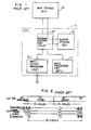
- As shown in Fig. 1, a large scale data processing system comprises a main storage (MS) 20 for storing data (instructions and operands) and a central processing unit (CPU) 10 which includes a basic processing unit (BPU) 11 for executing the instructions, a buffer storage (BS) 12 for storing a partial copy of the
MS 20, an input/output processor (IOP) 13 for controlling data transfer between an input/output unit (10) and theMS 20 and a storage control unit (SCU) 14 for controlling read and write operations of theMS 20 and theBS 12. - A difference of the configuration of Fig. 1 from small and middle scale information processing systems resides in that the
buffer storage 12 is provided and thestorage control unit 14 is an independent unit which executes and controls or buffers accesses to theMS 20 and theBS 12 when such accesses are requested simultaneously so that a data transfer ability is considerably increased. - The BS 12 is a small capacity, high speed memory unit. The content of the
MS 20 is divided into a plurality of sequential multi-byte (e.g. 64 bytes) blocks. The BS 12 stores a copy of the content of theMS 20 in a unit of the block. - Since the instructions and the operands for the program to be executed in the BPU 11 are fetched and read from the
BS 12 at a high speed, the execution time of the instructions is reduced. The result of the operation in the BPU 11 is again written in theBS 12 and also written in theMS 20. On the other hand, when data from theIOP 13 is to be stored, the data is written only to theMS 20, and if a block containing the data address has been registered in theBS 12, the registration is invalidated. Through those operations, the equality of the contents of theMS 20 and theBS 12 is assured. - When the address of the instruction or operand read request (access request) from the BPU 11 has not been registered in the
BS 12, a data block containing that address is transferred from theMS 20 and serially written in theBS 12. (This is called a block transfer). - In the large scale information processing system such as one shown in Fig. 1, various attempts to enhance the processing performance have been made. In one attempt, the instructions are pipeline- controlled so that the execution of the instruction which spreads over a number of cycles is done at a rate of one instruction per cycle.
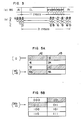
- Fig. 2 shows a sequence chart for a conventional control system as a whole.
- Fig. 2(a) shows status of the
BS 12 and Fig. 2(b) shows pipeline control stages of the instruction. In Fig. 2(b), the execution status of the instruction is shown by machine cycles (abscissa) for pipeline stages (ordinate) D (decode), A (address translation), L (load) and E (execution), and the sequence of the instruction executed is shown by CD (i=1, 2, 3,... ). The stage D is a decode stage which is carried out independently and in which an instruction is fetched from an instruction fetch control unit which supplies an instruction word and the fetched instruction is decoded. The stage A is an address translation stage in which a virtual address of an operand read request is translated to a real address and the registration of an area corresponding to the translated real address in theBS 12 is checked. The stage L is a data read stage in which an operand read request is issued to theBS 12 and the read operand is transferred to an arithmetic unit of the BPU 11. The stage E is an instruction execution stage in which the operand read by the arithmetic unit of the BPU 11 is processed, the result is checked and a store request of the result is issued to theBS 12 and theMS 20 or the result is loaded to a general purpose register or a floating point register. - In the most ideal case, each of the stages D through E can be completed in one cycle and the instructions can be sequentially executed. Accordingly, each instruction can be effectively executed. Accordingly, each instruction can be effectively executed in one cycle.
- The symbol CD indicates an indication time of the execution in the respective pipeline control stages. The position of the symbol (D, as it goes from left to right, shows the transition of the machine cycle time in the BPU 11 and the instruction execution status for the stages D through E.
- Fig. 2(a) shows the status of the
BS 12, that is, AV (available), CL (close) and WT (write). - In the status AV, the
BS 12 can accept the access request from the BPU 11. In the status CL, the access request from the BPU 11 is not accepted during the block transfer from theMS 20 because the access request was issued from the BPU 11 to theBS 12 but the corresponding data was not in the BS and the block transfer request has been issued to theMS 20. In the status WT, the access request from the BPU 11 is not accepted because the block data transferred from theMS 20 is being written to theBS 12. - In Figs. 2(a) and 2(b), the stages D, A, L and E for the first instruction CD are completed in one cycle, respectively, but the block transfer occurs for the read request to the
BS 12 by the second instruction ② because the requested operand has not been registered in theBS 12. - Assuming that a block size of the
BS 12 is 64 bytes, read data width of the data from theMS 20 is 8 bytes so that 8-byte data is transferred eight times and the block-transferred data is written in theBS 12 eight bytes at a time. Accordingly, one cycle is needed for every eight bytes and the status WT takes eight cycles. It is assumed that the status CL takes ten cycles. - The instruction or operand is transferred from the SCU 14 to the BPU 11 sixteen bytes at a time. When the first data and the second data of the block transfer are received from the
MS 20, a read termination signal is sent to the BPU 11 and the data is transferred. - Accordingly, the instruction ② shown in Fig. 2(b) waits for the termination of the operand read at the stage L, and at the third cycle from the beginning of the status WT, it can shift to the stage E. The instruction @ which instructs the readout from the
BS 12, however, is not completed in the status WT because the write status WT to theBS 12 due to the block transfer by the instruction @ continues for the eight cycles and it has to wait for six cycles in the stage L. The operand readout is completed when the status of theBS 12 shifts from WT to AV and the instruction @ can shift to the stage E. - In the prior art system, therefore, the time required from the initiation of the execution of the instruction (D to the termination of the execution of the instruction ② is only four cycles if all of the requested operands are in the
BS 12, but it is 21 cycles if the operand for the instruction @ is not in theBS 12. That is to say, the delay of the execution time due to the block transfer is 17 cycles (21-4=17) which materially reduces the processing performance of the information processing system. - By increasing the capacity of the
BS 12 to increase a probability of the presence of the requested data in theBS 12 in order to reduce the frequency of the block transfer, the processing performance may be increased. However, since the semiconductor devices used in theBS 12 must be of high performance, they are integrated in a low density, consume large power, are very expensive and must operate at a high speed. Accordingly, it is physically difficult to increase the capacity of theBS 12. - The EP-A-29 517 which is prior art according to article 54(3) EPC discloses a system capable of accessing a cache from a processor even during a line transfer. The known system is similar to the subject matter of the present invention according to claim 1 with the difference that the present invention allows that always n successive received data sub-units may be written simultaneously regardless of the bank in which the block transfer is started.
- In the EP-A-0 029 517 one line consists of 128 bytes (16 double words of information), and the one-block information is transferred by each unit of double words (DW) in sixteen times from the main storage to the cache. Thereby the manner of writing data into the cache is different depending on whether the first double word (DW 0) in a line fetch has an even address or an odd address. (Page 11, line 1 to
page 12, line 22 of the EP-A-0 029 517). That is, in this prior art, the cache can read or write four words (QW) at a time so that when the first double word DW of the line fetched has an even address, every four words are stored into the cache in a eight cycle sequence. However, when the first DW of the line has an odd address, thefirst DW 0 and the last DW 15 respectively are not written in the cache together with adjacent DW in one cycle, and theDW 0 and DW 15 are individually written alone. A nine-cycle sequence is required to write the 16 double words into the cache (page 11,line 10 to page 11, line 5 from the bottom and Figs. 10 and 11 of the EP-A-29 517). - The US―A―4 169 284 discloses a cache control for concurrent access which enables simultaneously access to the cache by main storage and the processor, the control performing two fast cycles during each processor cycle. In accordance with this control, high-speed elements or components are required for constructing the cache.
- The US―A―3 705 388 discloses a memory control system which enables access request during block transfer so that when an access request to the buffer memory is issued from the processor during a block transfer, the block transfer is interrupted temporarily.
- It is the object of the present invention to provide a data processing system which allows a buffer storage from a basic processing unit even during the block transfer, wherein double words in a block transfer are to be written into the buffer storage in a constant minimum cycle sequence, regardless of the address categorie of the first double word, e.g. odd address or even address. This should be effected also in the case alternate addresses are of multiple category, e.g. for n memory banks each having a different address category.
- The above object is solved according to the invention as claimed in claim 1 by a data processing system comprising
- a main storage for storing data sectioned into blocks each including a plurality of data bytes;
- a buffer storage for storing a copy of one of the blocks of said main storage as a unit; and
- control means for controlling read and write operations of said main storage and said buffer storage in response to a received access request and address;
- said main storage including means for transferring a block of data to said control means in sub-units of said unit during a plurality of successive transfer times, each sub-unit of data being transferred together with a first access request to write the block of data in said buffer storage;
- processor means for issuing a second access request and an address to said control means to read or write data from or into said buffer storage; and
- n data register means for buffering n data sub-units transferred in n successive transfer times where n is an integer equal to or greater than 2 from said main storage;
- said buffer storage including n memory bank means each being capable of operating independently from the other, and address register means provided for each memory bank means and for holding an address for each memory bank means, with successive addresses being sequentially distributed over the banks;
- said control means including accepting means for accepting as an access request to said buffer storage every n successive first access requests transferred to said control means from said main storage and for accepting receipt of said second access request from said processor means between said accepted n successive first access requests from said main storage so as to permit a buffer storage access by said processor means during a data block transfer from said main storage;
- said control means further including address modification and write means responsive to accepting of said n successive first access requests in said accepting means for setting addresses corresponding to the n successive first access requests into respective ones of said n address register means to write into said n memory bank means the data in said n data register means in one buffer store access cycle such that always n successive received data sub-units may be written simultaneously regardless of the bank in which the block transfer is started.
- The subclaims 2 and 3 characterize advantageous developments of claim 1 respectively.
- Thus, since the access request from the BPU is accepted during the block transfer, the performance is improved.
- The preferred embodiments of the present invention will be described with reference to the accompanying drawings in which:
- Fig. 1 shows a block diagram of a conventional data processing system,
- Fig. 2 shows a sequence chart for explaining the operation of the conventional data processing system,
- Fig. 3 shows a sequence chart for explaining a principle of the present invention,
- Fig. 4 shows a block diagram of one embodiment of the present invention,
- Figs. 5a and 5b illustrate sequences of transferred data to a BS shown in Fig. 4,
- Fig. 6 shows a detail of an address control circuit shown in Fig. 4, and
- Fig. 7 shows an access request selective accept circuit.
- Fig. 3 illustrates a principle of the present invention, and shows the status of the BS and the execution status of the instruction for each pipeline control stage when the same instruction as that of Fig. 2 is executed.
- In the present system, in order to relieve the reduction of the instruction execution ability due to the competition or collision of the block transfer request and the BPU access request, the configuration of the - data transfer path from the
MS 20 to theBS 12 in the block transfer is modified and the priority of the BPU access request and the block transfer request is controlled. - In the present invention, the unit of write to the
BS 12 is a plural number of times as large as that of the conventional system, that is, a plural number of times (for example, two times) as large as the data transfer width so that the block transferred data is written sixteen bytes at a time. As shown in the status WT in Fig. 3(a), the status AV which allows the acceptance of the BPU access request is established only for one cycle between the write cycle and the following write cycle. Consequently, following to the execution of the instruction @ which instructs the initiation of the block transfer, the operand for the instruction @ and the operands for the instructions @ and @ can be read so that the overall processing performance is improved. - In the conventional system shown in Fig. 2, four instructions are executed during 21 cycles starting from the initiation of the block transfer request while in the present system seven instructions are executed during the 21 cycles. Accordingly, the overhead of the block transfer is 17 cycles in the conventional system while it is 14 cycles in the present system.
- A probability of non-registration of the access request from the BPU 11 in the
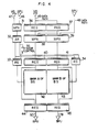
BS 12 is usually no less than 10% per instruction in the large program system although it depends on a particular program. Thus, an effective overhead of the block transfer is equal to a product of the overhead of the block transfer (14 cycles) times the probability (10%), that is, 1.4 cycles per instruction. In the conventional system, the effective overhead is equal to a product of 17cycles times 10%, that is, 1.7 cycles. Accordingly, the present invention can increase the processing speed by 0.3 cycles per instruction. Since one instruction is executed in four cycles in average, the processing performance is improved by approximately 8% in the present invention. - Fig. 4 shows a block diagram of BS's and peripheral circuits in one embodiment of the present invention.
- A bank A of
BS 42 and a bank B ofBS 43 can read and write eight-byte (doubleword) data and can be independently accessed by addresses loaded in aregister 33 and aregister 34, respectively. A doubleword data to be stored in thebank A 42 is loaded in aregister 40, and a doubleword data to be stored in thebank B 43 is loaded in aregister 41. The doubleword data read from thebank A 42 and thebank B 43 are loaded toregisters 44 and 45, respectively. The addressing to thebank A 42 and thebank B 43 is done alternately by the unit of eight. That is, addresses 0-7 are allotted to thebank A 42, the following addresses 8-15 are allotted to thebank B 43, the addresses 16-23 are allotted to thebank A 42, the addresses 24-31 are allotted to thebank B 43 and so on. For example, when the address in theregister 33 is one of 0-7, the eight bytes of the corresponding address 0-7 are parallelly read from thebank A 42 and loaded to theregister 44. - When the BPU issues an access request, the address is supplied to a multiplexor (MPX) 31 through a path 46 and the store data is supplied to a multiplexor (MPX) 38 or 39 through a
path 48. - On the other hand, when the MS issues a block transfer request, the address is supplied to a multiplexor (MPX) 31 through a
path 47 and the block data is supplied to registers (REG) 36 and 37 through apath 49. - The block transfer request from the MS and the access request from the BPU are selectively accepted and the address supplied through the
path 46 or 47 is selected by themultiplexor 31 and supplied to an address register (AR) 32. The acceptance of the access request will be explained later in connection with Fig. 7. The content of theaddress register 32 is supplied to the tworegisters register 33 through anaddress control circuit 35. Theaddress control circuit 35 will be explained later in conjunction with Fig. 6. It does not modify the address bits when a 23-bit of the address in theregister 32 is "0" (that is, when the doubleword address excluding three low order bits of the address is even) and adds eight to the address when the 23 bit is "1" (that is, when the doubleword address excluding the three low order bits of the address is odd). - When the write data is sent from the BPU, eight bytes at a time, through the
path 48, either one of themultiplexors 38 or 39 is selected and the content thereof is loaded to theregister BS multiplexor 38 and theregister 40 are selected and the data is written at the address specified by theaddress register 33, and when the write address is an odd doubleword address, themultiplexor 31 and theregister 41 are selected and the data is written at the address specified by theaddress register 34. - The block transfer data is sent from the MS through the
path 49 in eight cycles, 8 bytes in each cycle. The block transfer from the MS to the BS is done first to the address requested by the block transfer request and then to incremental interblock addresses. The interblock addresses can be represented by six bits (26=64) when the block size is 64 bytes. Since the data is written in thebanks - When the block transfer is to start from an even doubleword address, the
even bank 42 and theodd bank 43 of the BS are paired, and when the block transfer is to start from an odd doubleword address, the odd bank and theeven bank 42 are paired. - Figs. 5a and 5b illustrate the write sequence of the block transferred data to the BS shown in Fig. 4. Eig. 5a illustrates in decimal notation while Fig. 5b illustrates in binary notation.
- In the BS shown in Figs. 5a and 5b, the data at the interblock high order address "000" is stored at the addresses 0-7 in the
odd bank 42, the data at the interblock high order address "001" is stored at the address 8-15 in theodd bank 43, the data at the interblock high order address "010" is stored at the addresses 16-23 in theeven bank 42 and so on. - If the block transfer starts from the even doubleword address, for example "000", the addresses 0-7 of the
even bank 42 and the addresses 8-15 of theodd bank 43 are paired so that sixteen bytes are parallelly written in the BS (as shown by hatched areas). If the block transfer starts from the odd doubleword address, for example "101", the addresses 40-47 of theodd bank 43 and the addresses 48-55 of theeven bank 42 are paired so that sixteen bytes are parallelly written in the BS (as shown by hatched areas). - When the block transfer starts from the odd doubleword address, the write address for the
even bank 42 of the BS is larger than that of theodd bank 43 by eight (or one as viewed from the interblock high order address). - Referring to Fig. 5b which shows the interblock high order address in binary notation, when the 64-byte data write starts from the bank "001", the banks "001" and "010", the banks "011" and "100", the banks "101" and "110" and the banks "111" and "000" are paired respectively and the data is written in four cycles.
- The
address control circuit 35 controls the addressing. When the block transfer address from the MS or the read address from the BPU is loaded to theaddress register 32 shown in Fig. 4, theaddress control circuit 35 checks the fourth bit (23 bit) in the interblock address counted from the least significant bit to determine if it is "1" or "0", and if it is "0", the interblock address is loaded to theregister 33, and if it is "1", the interblock address is incremented by eight and the incremented address is loaded to theregister 33. In this manner, it is determined if the first interblock high order address is even or odd, and if it is even, the address to be loaded to theregister 33 need not be modified because theeven bank 42 and theodd bank 43 are paired, and if it is odd, the address incremented by eight by theaddress control circuit 35 is loaded to theregister 33 because theeven bank 42 which is one row lower than theodd bank 43 is used to write the data. - Fig. 6 shows a logic circuit for the address modification in the
address control circuit 35 of Fig. 4. - The
address control circuit 35 modifies two high order bits of the interblock high order address. Referring to Fig. 6, AR (3, 2) indicates a second bit of a third byte of the address, AND denotes an AND gate and OR denotes an OR gate. - Three bits AR (3, 2), AR (3, 3) and AR (3, 4) which are the interblock high order address of the output from the
address register 32 shown in Fig. 4 are supplied to the logic circuit of Fig. 6, which produces output data RGIN (3, 2) and RGIN (3, 3) to theregister 33 for the memory bank of the BS. - The relation between AR (3, 2), AR (3, 3), AR (3, 4) and RGIN (3, 2), RGIN (3, 3) is shown below.
-

- Other bits are not modified. As seen from the above table, when the bit AR (3, 4) or the 23 bit is "0", AR (3, 2) and AR (3, 3) appear as RGIN (3, 2) and RGIN (3, 3) without modification, and when it is "1", they are incremented by eight.
- Referring again to Fig. 4, the transfer of the data address and the write of data in the BS during the block transfer and the data transfer to the BPU are explained.
- For example, when the interblock high order address is "001" and the data requested by the access request from the BPU has not been registered in the BS, the block transfer from the MS starts. As the access to the MS has been accepted and the data is sequentially transferred from the MS to the BS, the first data at the interblock high order address "001" is first loaded to the
register 37 through thepath 49. The address circuit and the BS are not affected at this time. - In the second cycle, the second data at the next interblock high order address "010" is sent through the path 149 and loaded to the
register 36. The address is simultaneously supplied through thepath 47. - The SCU preferentially handles the block transfer request so that the
path 47 is selected by themultiplexor 31 and the address is loaded to theregister 32. - Then, the contents of the
registers registers multiplexors 39 and 38 and are also loaded to theregisters 45 and 44, respectively. Theregisters banks registers 45 and 44 retain the read data to be transferred to the BPU. - On the other hand, the address in the
register 32 is loaded to theregisters address control circuit 35 is loaded to theregister 33. When the addresses are supplied to thebanks register 41 is written in thebank 43 and the 8-byte data in theregister 40 is written in thebank 42. The contents of theregisters 45 and 44 are fed to the BPU as the instruction or the operand. - In the third cycle, the data at the interblock high order address "011" is supplied to the
register 37 through thepath 49. The address circuit, the BS and theregisters 44 and 45 are used to handle the access request from the BPU. Themultiplexor 31 selects the path 46 and the multiplexors 38 and 39 select thepath 48. - In the fourth cycle, the data at the interblock high order address "100" is transferred to the
register 36. The data is then written in thebanks - In the fifth cycle, the data at the interblock high order address "101" is transferred. The
multiplexors paths 46 and 48 to accept the access request from the BPU. - In the sixth cycle, the block transfer of the data at the interblock high order address "110" is accepted and the data at the interblock high order addresses "101" and "110" are written in the BS.
- As seen from the above, the
registers - In this manner, the block transfer and the BPU access request are alternately handled.
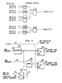
- Fig. 7 shows an example of an access request selective accept circuit.
- A logic circuit shown in Fig. 7 is used to selectively accept the block transfer request from the MS and the access request from the BPU.
- The block transfer request from the MS is supplied to a
counter 81 through apath 72. When the counter 81 counts two access requests, it produces a "1" output which is fed to a data input terminal D of a flip-flop 84. This signal is sampled when a clock supplied through a path 71 is "1" to produce a "1" output on apath 78. Accordingly, for every two access requests transferred from the MS, one access request is accepted. The signal on thepath 78 selects themultiplexors - A flip-
flop 83 indicates the status CL shown in Fig. 3. It is set by a signal on apath 75 which is present when the data requested by the BPU is not in the BS and the block transfer is requested to the MS, and reset by the initiation of the block transfer. The reset output of the flip-flop 83 is supplied to an ANDgate 82 through apath 77. - The access request from the BPU is supplied to the AND
gate 82 through apath 73. When the output signal of the counter is "0" and the flip-flop 77 is reset, the ANDgate 82 is opened to set a flip-flop 85 to produce a "1" output on a path 79 so that the access request from the BPU is accepted. The signal on the path 79 selects themultiplexors - In the illustrated embodiment, the eight-
byte registers - While the block transfer is effected serially eight bytes at a time and the write to the BS is effected sixteen bytes at a time in the illustrated embodiment, the present invention is not limited to the specific embodiment and the byte width may be variable.
Claims (3)
Applications Claiming Priority (2)
| Application Number | Priority Date | Filing Date | Title |
|---|---|---|---|
| JP55182543A JPS57105879A (en) | 1980-12-23 | 1980-12-23 | Control system for storage device |
| JP182543/80 | 1980-12-23 |
Publications (3)
| Publication Number | Publication Date |
|---|---|
| EP0054888A2 EP0054888A2 (en) | 1982-06-30 |
| EP0054888A3 EP0054888A3 (en) | 1984-07-04 |
| EP0054888B1 true EP0054888B1 (en) | 1987-11-25 |
Family
ID=16120121
Family Applications (1)
| Application Number | Title | Priority Date | Filing Date |
|---|---|---|---|
| EP81110452A Expired EP0054888B1 (en) | 1980-12-23 | 1981-12-15 | Data-processing system with main and buffer storage control |
Country Status (4)
| Country | Link |
|---|---|
| US (1) | US4467419A (en) |
| EP (1) | EP0054888B1 (en) |
| JP (1) | JPS57105879A (en) |
| DE (1) | DE3176548D1 (en) |
Families Citing this family (36)
| Publication number | Priority date | Publication date | Assignee | Title |
|---|---|---|---|---|
| BR8406089A (en) * | 1983-11-30 | 1985-09-24 | Fujitsu Ltd | PROCESS TO CONTROL INTERMEDIATE MEMORY IN DATA PROCESSING DEVICE |
| US4680702A (en) * | 1984-04-27 | 1987-07-14 | Honeywell Information Systems Inc. | Merge control apparatus for a store into cache of a data processing system |
| US4663728A (en) * | 1984-06-20 | 1987-05-05 | Weatherford James R | Read/modify/write circuit for computer memory operation |
| JPS618785A (en) * | 1984-06-21 | 1986-01-16 | Fujitsu Ltd | Access control system for storage device |
| EP0189944B1 (en) * | 1985-02-01 | 1993-05-12 | Nec Corporation | Cache memory circuit capable of processing a read request during transfer of a data block |
| US4685082A (en) * | 1985-02-22 | 1987-08-04 | Wang Laboratories, Inc. | Simplified cache with automatic update |
| JPS61224051A (en) * | 1985-03-29 | 1986-10-04 | Fujitsu Ltd | Buffer memory control system |
| JPS62102344A (en) * | 1985-10-29 | 1987-05-12 | Fujitsu Ltd | Buffer memory control system |
| JPS6356754A (en) * | 1986-08-28 | 1988-03-11 | Toshiba Corp | Input/output channel |
| CA1300759C (en) * | 1987-02-07 | 1992-05-12 | Kouji Kinoshita | Buffer memory circuit arrangement capable of receiving a requestwithout qualification during block transfer |
| EP0280954B1 (en) * | 1987-02-16 | 1991-04-24 | Siemens Aktiengesellschaft | Data exchange control method between processing units and a memory arrangement including a cache in data-processing systems, as well as a cache operating according to this method |
| JP2561261B2 (en) * | 1987-02-18 | 1996-12-04 | 株式会社日立製作所 | Buffer storage access method |
| US5081701A (en) * | 1987-04-20 | 1992-01-14 | Tandem Computers Incorporated | System for controlling data transfer using transfer handshake protocol using transfer complete and transfer inhibit signals |
| JPH0740244B2 (en) * | 1987-08-05 | 1995-05-01 | 三菱電機株式会社 | Micro Processor |
| US4910656A (en) * | 1987-09-21 | 1990-03-20 | Motorola, Inc. | Bus master having selective burst initiation |
| US4816997A (en) * | 1987-09-21 | 1989-03-28 | Motorola, Inc. | Bus master having selective burst deferral |
| GB2216305A (en) * | 1988-03-01 | 1989-10-04 | Ardent Computer Corp | Cache block transfer in a computer system |
| US5212780A (en) * | 1988-05-09 | 1993-05-18 | Microchip Technology Incorporated | System for single cycle transfer of unmodified data to a next sequentially higher address in a semiconductor memory |
| US4918696A (en) * | 1988-09-19 | 1990-04-17 | Unisys Corporation | Bank initiate error detection |
| JP3081614B2 (en) * | 1989-03-08 | 2000-08-28 | 富士通株式会社 | Partial write control device |
| US5117486A (en) * | 1989-04-21 | 1992-05-26 | International Business Machines Corp. | Buffer for packetizing block of data with different sizes and rates received from first processor before transferring to second processor |
| US5155832A (en) * | 1989-07-05 | 1992-10-13 | Hewlett-Packard Company | Method to increase performance in a multi-level cache system by the use of forced cache misses |
| US4998221A (en) * | 1989-10-31 | 1991-03-05 | International Business Machines Corporation | Memory by-pass for write through read operations |
| US5434990A (en) * | 1990-08-06 | 1995-07-18 | Ncr Corporation | Method for serially or concurrently addressing n individually addressable memories each having an address latch and data latch |
| EP0473804A1 (en) * | 1990-09-03 | 1992-03-11 | International Business Machines Corporation | Alignment of line elements for memory to cache data transfer |
| EP0575651A1 (en) * | 1992-06-24 | 1993-12-29 | International Business Machines Corporation | Multiprocessor system |
| JPH0756815A (en) * | 1993-07-28 | 1995-03-03 | Internatl Business Mach Corp <Ibm> | Cache operating method and cache |
| US5553265A (en) * | 1994-10-21 | 1996-09-03 | International Business Machines Corporation | Methods and system for merging data during cache checking and write-back cycles for memory reads and writes |
| JPH08314794A (en) * | 1995-02-28 | 1996-11-29 | Matsushita Electric Ind Co Ltd | Method and system for shortening wait time of access to stable storage device |
| US7213103B2 (en) * | 2004-04-22 | 2007-05-01 | Apple Inc. | Accessing data storage systems without waiting for read errors |
| US7577763B1 (en) | 2005-02-28 | 2009-08-18 | Apple Inc. | Managing read requests from multiple requestors |
| US7523146B2 (en) * | 2005-06-21 | 2009-04-21 | Apple Inc. | Apparatus and method for peer-to-peer N-way synchronization in a decentralized environment |
| US8495015B2 (en) * | 2005-06-21 | 2013-07-23 | Apple Inc. | Peer-to-peer syncing in a decentralized environment |
| US7797670B2 (en) * | 2006-04-14 | 2010-09-14 | Apple Inc. | Mirrored file system |
| US7860826B2 (en) | 2006-08-04 | 2010-12-28 | Apple Inc. | Method and system for using global equivalency sets to identify data during peer-to-peer synchronization |
| US7657769B2 (en) | 2007-01-08 | 2010-02-02 | Marcy M Scott | N-way synchronization of data |
Family Cites Families (11)
| Publication number | Priority date | Publication date | Assignee | Title |
|---|---|---|---|---|
| FR1541240A (en) * | 1966-11-10 | Ibm | Overlap and interleave access for multi-speed memories | |
| US3618041A (en) * | 1968-10-31 | 1971-11-02 | Hitachi Ltd | Memory control system |
| US3588829A (en) * | 1968-11-14 | 1971-06-28 | Ibm | Integrated memory system with block transfer to a buffer store |
| US3611307A (en) * | 1969-04-03 | 1971-10-05 | Ibm | Execution unit shared by plurality of arrays of virtual processors |
| US3705388A (en) * | 1969-08-12 | 1972-12-05 | Kogyo Gijutsuin | Memory control system which enables access requests during block transfer |
| US3771137A (en) * | 1971-09-10 | 1973-11-06 | Ibm | Memory control in a multipurpose system utilizing a broadcast |
| FR129151A (en) * | 1974-02-09 | |||
| US3967247A (en) * | 1974-11-11 | 1976-06-29 | Sperry Rand Corporation | Storage interface unit |
| US4169284A (en) * | 1978-03-07 | 1979-09-25 | International Business Machines Corporation | Cache control for concurrent access |
| US4323968A (en) * | 1978-10-26 | 1982-04-06 | International Business Machines Corporation | Multilevel storage system having unitary control of data transfers |
| US4317168A (en) * | 1979-11-23 | 1982-02-23 | International Business Machines Corporation | Cache organization enabling concurrent line castout and line fetch transfers with main storage |
-
1980
- 1980-12-23 JP JP55182543A patent/JPS57105879A/en active Pending
-
1981
- 1981-12-15 DE DE8181110452T patent/DE3176548D1/en not_active Expired
- 1981-12-15 EP EP81110452A patent/EP0054888B1/en not_active Expired
- 1981-12-17 US US06/331,895 patent/US4467419A/en not_active Expired - Fee Related
Also Published As
| Publication number | Publication date |
|---|---|
| US4467419A (en) | 1984-08-21 |
| JPS57105879A (en) | 1982-07-01 |
| EP0054888A2 (en) | 1982-06-30 |
| DE3176548D1 (en) | 1988-01-07 |
| EP0054888A3 (en) | 1984-07-04 |
Similar Documents
| Publication | Publication Date | Title |
|---|---|---|
| EP0054888B1 (en) | Data-processing system with main and buffer storage control | |
| US4131940A (en) | Channel data buffer apparatus for a digital data processing system | |
| US4866603A (en) | Memory control system using a single access request for doubleword data transfers from both odd and even memory banks | |
| US4354232A (en) | Cache memory command buffer circuit | |
| US5590353A (en) | Vector processor adopting a memory skewing scheme for preventing degradation of access performance | |
| US4888679A (en) | Method and apparatus using a cache and main memory for both vector processing and scalar processing by prefetching cache blocks including vector data elements | |
| US4648034A (en) | Busy signal interface between master and slave processors in a computer system | |
| US6272596B1 (en) | Data processor | |
| CA1089107A (en) | Channel bus controller | |
| JPS61109146A (en) | Advanced control system | |
| JPS59117666A (en) | Vector processor | |
| EP0170284B1 (en) | Microcomputer | |
| JPH02149156A (en) | Communication processor | |
| JPH0463430B2 (en) | ||
| US5440717A (en) | Computer pipeline including dual-ported, content-addressable writebuffer | |
| US4639862A (en) | Computer system | |
| EP0437160B1 (en) | Main storage memory cards having single bit set and reset functions | |
| JP2561261B2 (en) | Buffer storage access method | |
| EP0010196B1 (en) | Control circuit and process for digital storage devices | |
| EP0473804A1 (en) | Alignment of line elements for memory to cache data transfer | |
| US4737908A (en) | Buffer memory control system | |
| US6349370B1 (en) | Multiple bus shared memory parallel processor and processing method | |
| US5247695A (en) | Vector processor with byte access of memory | |
| JP3956652B2 (en) | Processor system | |
| JPH0232648B2 (en) |
Legal Events
| Date | Code | Title | Description |
|---|---|---|---|
| PUAI | Public reference made under article 153(3) epc to a published international application that has entered the european phase |
Free format text: ORIGINAL CODE: 0009012 |
|
| AK | Designated contracting states |
Designated state(s): DE FR GB IT |
|
| PUAL | Search report despatched |
Free format text: ORIGINAL CODE: 0009013 |
|
| AK | Designated contracting states |
Designated state(s): DE FR GB IT |
|
| 17P | Request for examination filed |
Effective date: 19841128 |
|
| GRAA | (expected) grant |
Free format text: ORIGINAL CODE: 0009210 |
|
| AK | Designated contracting states |
Kind code of ref document: B1 Designated state(s): DE FR GB IT |
|
| REF | Corresponds to: |
Ref document number: 3176548 Country of ref document: DE Date of ref document: 19880107 |
|
| ET | Fr: translation filed | ||
| ITF | It: translation for a ep patent filed |
Owner name: MODIANO & ASSOCIATI S.R.L. |
|
| PLBE | No opposition filed within time limit |
Free format text: ORIGINAL CODE: 0009261 |
|
| STAA | Information on the status of an ep patent application or granted ep patent |
Free format text: STATUS: NO OPPOSITION FILED WITHIN TIME LIMIT |
|
| 26N | No opposition filed | ||
| PGFP | Annual fee paid to national office [announced via postgrant information from national office to epo] |
Ref country code: FR Payment date: 19901109 Year of fee payment: 10 |
|
| PGFP | Annual fee paid to national office [announced via postgrant information from national office to epo] |
Ref country code: GB Payment date: 19901205 Year of fee payment: 10 |
|
| ITTA | It: last paid annual fee | ||
| PGFP | Annual fee paid to national office [announced via postgrant information from national office to epo] |
Ref country code: DE Payment date: 19910107 Year of fee payment: 10 |
|
| PG25 | Lapsed in a contracting state [announced via postgrant information from national office to epo] |
Ref country code: GB Effective date: 19911215 |
|
| GBPC | Gb: european patent ceased through non-payment of renewal fee | ||
| PG25 | Lapsed in a contracting state [announced via postgrant information from national office to epo] |
Ref country code: FR Effective date: 19920831 |
|
| PG25 | Lapsed in a contracting state [announced via postgrant information from national office to epo] |
Ref country code: DE Effective date: 19920901 |
|
| REG | Reference to a national code |
Ref country code: FR Ref legal event code: ST |