EP0054864A2 - Reflektoranordnung für eine Blitzlichteinheit - Google Patents
Reflektoranordnung für eine Blitzlichteinheit Download PDFInfo
- Publication number
- EP0054864A2 EP0054864A2 EP81110356A EP81110356A EP0054864A2 EP 0054864 A2 EP0054864 A2 EP 0054864A2 EP 81110356 A EP81110356 A EP 81110356A EP 81110356 A EP81110356 A EP 81110356A EP 0054864 A2 EP0054864 A2 EP 0054864A2
- Authority
- EP
- European Patent Office
- Prior art keywords
- cavity
- planar
- reflector
- lamp
- cavities
- Prior art date
- Legal status (The legal status is an assumption and is not a legal conclusion. Google has not performed a legal analysis and makes no representation as to the accuracy of the status listed.)
- Granted
Links
Images

Classifications
-
- G—PHYSICS
- G03—PHOTOGRAPHY; CINEMATOGRAPHY; ANALOGOUS TECHNIQUES USING WAVES OTHER THAN OPTICAL WAVES; ELECTROGRAPHY; HOLOGRAPHY
- G03B—APPARATUS OR ARRANGEMENTS FOR TAKING PHOTOGRAPHS OR FOR PROJECTING OR VIEWING THEM; APPARATUS OR ARRANGEMENTS EMPLOYING ANALOGOUS TECHNIQUES USING WAVES OTHER THAN OPTICAL WAVES; ACCESSORIES THEREFOR
- G03B15/00—Special procedures for taking photographs; Apparatus therefor
- G03B15/02—Illuminating scene
- G03B15/03—Combinations of cameras with lighting apparatus; Flash units
- G03B15/04—Combinations of cameras with non-electronic flash apparatus; Non-electronic flash units
- G03B15/0442—Constructional details of the flash apparatus; Arrangement of lamps, reflectors, or the like
Definitions
- This invention relates to photoflash units and, more . particularly to compact reflector-lamp modules and multilamp photoflash arrays having a multiplicity of such reflector-lamp modules in close-nested relationship.
- multi lamp photoflash units may be characterized as either cube or linear array configurations.
- Cube unit configurations are illustrated by U.S. Patent No. 3,730,669, referred to as magicube.
- a linear array configuration is depicted in U.S. Patent No. 3,857,667, referred to as a flashbar, and planar array configurations are shown in U.S. Patents Nos. 3,894,226 and 4,017,728, referred to as a flip flash.
- the method of measuring light distribution across the photographic zone is by comparing the light output in the center 5° to the average output of a 5° zone between 15° and 20° inside the perimeter of the picture area.
- prior art lamp reflector modules have provided a distribution between 1.6:1 and 2:1. This means that the center has nearly twice the exposure of the edge; this is nearly a full f-stop setting on the camera lens.
- a distribution ratio of 1:1 is desired; however, even a bare (unreflected) lamp will provide a distribution of about 1.3:1 because of the cosine law of light distribution. Elimination of a focusing reflector, of course, results in a significant loss of light output. Hence, in practice, a lamp-reflector system providing a 1.3:1 ratio of light distribution would be a significant improvement in light uniformity while retaining a degree of output enhancement.
- U.S. Patent 3,860,809 describes a lamp-reflector combination wherein the ratio of the width of the reflector opening-tolamp envelope diameter is from about 1.2 to 2. Further the reflector is described as having an arcuate rear wall portion that is in nested relationship with the lamp envelope and has substantially flat outwardly diverging sidewall segments.
- U.S. Patent 3,991,308 shows a reflector having a cylindrical central portion and flat side portions.
- U.S. Patent 3,267,272 shows a reflector with a substantially V-shaped cross-section.
- the simplest and least costly method of producing reflectors is by thermo-vacuum-forming of thin, thermoplastic film. With reduced ratios of reflector opening-to-lamp diameter, however, excessive thinning of the rear portion of the reflector results.
- the aforementioned planar rear section design with single flat sides exager- ates the problem even further; for example, we have observed plastic thinning at the corners of the cavity walls whereby the minimum thickness is less than 10% of the maximum thickness. The smaller the reflector opening-to-lamp diameter or, conversely, the larger the lamp diameter-to-reflector opening, the greater the plastic thinning.
- An object of the present invention is to provide improved reflector-lamp modules for photoflash lamp devices, such as multi- lamps photoflash arrays. Another object of the invention is to provide an improved multilamp photoflash unit having a more compact reflector opening-to-lamp diameter ratio with improved structural integrity and light output. Still another object of the invention is to provide a multilamp photoflash unit which is economical to fabricate and provides enhanced packaging capabilities.
- a photoflash device comprising a reflector and flashlamp combination wherein the flashlamp has a tubular envelope; the reflector has surfaces forming a lamp receiving cavity and defining a front opening; and the lamp is nested within the reflector cavity with the longitudinal axis of the lamp parallel to the longitudinal axis of the reflector cavity, with the width of the reflector opening-to-diameter of the lamp envelope being less than about 1.2.
- the reflector cavity comprises a planar rear wall section joined to a pair of oppositely disposed bi-planar side wall sections.
- the lamp and reflector combination is employed in a multilamp photoflash unit including a housing means having a back portion containing a plurality of lamp-receiving reflective cavities.
- a plurality of flashlamps each having a tubular envelope are longitudinally disposed in respective ones of the reflective cavities, as mentioned above, and the ratio of the width of each cavity opening to the diameter of the lamp contained therein is less than about 1.2.
- a light-transmitting front portion of the - housing means is attached to the back portion and covers the cavity openings to enclose the lamps.
- Each cavity preferably comprises a planar rear wall section and a pair-of bi-planar sidewall sections.
- the housing back portion is a formed sheet of plastic film with the cavities formed therein.
- plastic thinning of each cavity wall is reduced, whereby the minimum thickness is greater than one-quarter the maximum thickness, thereby maintaining structural integrity.
- the front portion of the housing means is substantially planar and contiguous with the front surfaces of the plurality of lamp envelope.
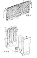
- FIGS. 1 and 2 illustrate a multilamp photoflash unit which includes a housing member 7, a multiplicity of flashlamps 9 disposed wihin the housing member 7 and a printed circuit board 11 positioned to extend into the housing member 7.
- the printed circuit board 11 includes terminals lla electrically coupled to the flashlamps 9 and provides for external access of electrical energy to the flahlamps 9 within the housing member 7.
- the housing member 7 has a back portion 13 . formed to provide a plurality of cavities 15 disposed in a planar array facing in one direction, in this embodiment.
- Each of the cavities 15 is or has affixed thereto a reflective surface 16 which includes a planar rear wall section 17 and a pair of oppositely- disposed bi-planar side wall sections 19 and 21.
- the bi-planar side sections 19 and 21 are affixed to and extend outwardly from the planar rear section 17 to form a reflective surface opening 23.
- This printed circuit board 11 Positionally located to contact, or join, the back portion 13 of the housing member 7 is the printed circuit board 11. This printed circuit board 11 extends inwardly of at least a portion of the multiplicity of cavities 15 and provides electrical access thereto from an energy source external to the housing member 7.
- each flashlamp 9 has a tubular envelope disposed within each of the cavities 15 contiguous to the reflective surface 16, and the longitudinal axis of each lamp envelope is disposed parallel to the longitudinal axis of the reflector cavity.
- Each of the flashlamps 9 includes a pair of lead wires 27 which are formed for connection to the printed circuit board 11 and serve to provide a path for energization of the flashlamp 9 by way of the printed circuit board 11.
- the housing member 7 includes a light-transmitting front portion 29 which is attached to the back section 13.
- This substantially planar front portion 29 covers openings 23 and encloses the flashlamps 9 within the cavities 15.
- the front portion 29 has a rearwardly directed web 31 which encloses and protects the connections of the lead wires 27 of the flashlamps 9 to the printed circuit board 11.
- FIG. 3 a cross-sectional view of a multilamp photoflash unit having a horizontal linear array of aligned cavities 15 each containing a flashlamp 9 is illustrated in FIG. 3.
- a single reflector or lamp module is shown in FIG. 4.
- each of the cavities 15 has a reflective surface 16 contiguous to the flashlamps 9 and is formed to provide a reflective surface opening 23.
- the reflective surface 16 of the cavities 15 includes a planar rear wall section 17.
- the above-mentioned planar rear wall section 17 has a recessed lower portion 17a for accomodation of projections (not shown) from the printed circuit board 11.
- each of these bi-planar sidewall sections 19 and 21 includes a pair of juxtaposed longitudinal planar segments 19a and 19b and 21a and 21b which may be but not necessarily need be of the same size.
- the segments 19a and 19b are joined to form an obtuse angle between the surfaces thereof within the cavity, and the segments 21a and 21b are joined in like manner.
- Each lamp is then nested in a respective reflector, as best shown in FIG. 4, with the tubular lamp envelope having portions contiguous with the rear wall section 17 and all of the sidewall planar segments 19a, 19b, 21a and 21b.
- the aperture plane of each reflector cavity represented by the position of the front housing portion 29, is substantially contiguous with the front surface of each lamp envelope 9, as shown in FIGS. 7 and 4.
- the bi-planar sidewall sections 19 and 21 extend outwardly from the planar rear wall section 17 to form the reflective surface opening 23. Moreover, this reflective surface opening 23 for each of the cavities 15 has a width dimension such that the ratio thereof to the diameter of a flashlamp 9 is less than about 1.2.
- thermovacuum-forming technique utilizing a thin, thermoplastic film.
- thermovacuum-forming to provide a planar rear wall section 17 and a reflector opening-to-depth ratio of less than about 1.2 tends to cause excessive thinning of the sidewall corners forming the rear wall section 17.
- the reflector cavities were thermovacuum-formed in a sheet of polyvinyl chloride with a maximum wall thickness of 15 mils.
- the height of each reflector cavity was about 1-1/8 inch.
- the width of each reflector opening was about 0.370 inch, and the outside diameter of each lamp envelope (lacquer coated glass) was about 0.320 to 0.330 inch.
- the ratio of reflector width opening-to-lamp diameter was about 1.16 to 1.12.
- the typical maximum and minimum wall thicknesses for each cavity were about 14 mils and 4 mils, respectively.
- the light distribution was about 1.3:1 and the total light output was about 330 zonal lumen-seconds.
- a multilamp-photoflash unit which includes a plurality of cavities aligned in a single plane with each cavity including a reflective surface having a width of reflective surface opening to flashlamp diameter ratio of less than about 1.2.
- the unit not only provides an enhanced uniformity and increased intensity of light on a photographic exposure area, due to the minimized ratio of reflector opening to lamp diameter together with a planar rear wall section, but the unit also provides greatly improved packaging capability in reduced space, while retaining structural integrity, due to the bi-planar sidewall configuration.
Landscapes
- Physics & Mathematics (AREA)
- General Physics & Mathematics (AREA)
- Stroboscope Apparatuses (AREA)
Applications Claiming Priority (2)
| Application Number | Priority Date | Filing Date | Title |
|---|---|---|---|
| US06/217,721 US4371913A (en) | 1980-12-18 | 1980-12-18 | Reflector lamp module for photoflash array |
| US217721 | 1988-07-11 |
Publications (3)
| Publication Number | Publication Date |
|---|---|
| EP0054864A2 true EP0054864A2 (de) | 1982-06-30 |
| EP0054864A3 EP0054864A3 (en) | 1982-09-29 |
| EP0054864B1 EP0054864B1 (de) | 1986-04-16 |
Family
ID=22812225
Family Applications (1)
| Application Number | Title | Priority Date | Filing Date |
|---|---|---|---|
| EP81110356A Expired EP0054864B1 (de) | 1980-12-18 | 1981-12-11 | Reflektoranordnung für eine Blitzlichteinheit |
Country Status (5)
| Country | Link |
|---|---|
| US (1) | US4371913A (de) |
| EP (1) | EP0054864B1 (de) |
| JP (1) | JPS57129425A (de) |
| CA (1) | CA1181727A (de) |
| DE (1) | DE3174428D1 (de) |
Families Citing this family (3)
| Publication number | Priority date | Publication date | Assignee | Title |
|---|---|---|---|---|
| JPS57162202A (en) * | 1981-03-30 | 1982-10-06 | Fuji Photo Optical Co Ltd | Bar-shaped electronic light emitting device |
| US4581682A (en) * | 1985-03-06 | 1986-04-08 | Gte Products Corporation | Prismatic sympathetic flash barriers |
| US6270228B1 (en) | 1999-03-31 | 2001-08-07 | Astron Systems, Inc. | Studio lighting system |
Family Cites Families (7)
| Publication number | Priority date | Publication date | Assignee | Title |
|---|---|---|---|---|
| US3454756A (en) * | 1966-07-14 | 1969-07-08 | Tokyo Shibaura Electric Co | Flash bulb magazine |
| NL7016259A (de) * | 1970-11-06 | 1972-05-09 | ||
| US3860809A (en) * | 1973-07-17 | 1975-01-14 | Westinghouse Electric Corp | Photoflash lamp-reflector module and miniature multiflash units for photographic cameras |
| NL7313364A (nl) * | 1973-09-28 | 1975-04-02 | Philips Nv | Flitslampeneenheid. |
| US4155110A (en) * | 1977-09-01 | 1979-05-15 | Gte Sylvania, Incorporated | Reflector-lamp module for photoflash array |
| US4136377A (en) * | 1978-02-16 | 1979-01-23 | Gte Sylvania Incorporated | Foldable photoflash lamp unit |
| US4243371A (en) * | 1978-03-13 | 1981-01-06 | General Electric Company | Flash lamp array construction |
-
1980
- 1980-12-18 US US06/217,721 patent/US4371913A/en not_active Expired - Fee Related
-
1981
- 1981-12-10 CA CA000391984A patent/CA1181727A/en not_active Expired
- 1981-12-11 DE DE8181110356T patent/DE3174428D1/de not_active Expired
- 1981-12-11 EP EP81110356A patent/EP0054864B1/de not_active Expired
- 1981-12-17 JP JP56202579A patent/JPS57129425A/ja active Pending
Also Published As
| Publication number | Publication date |
|---|---|
| CA1181727A (en) | 1985-01-29 |
| EP0054864B1 (de) | 1986-04-16 |
| US4371913A (en) | 1983-02-01 |
| JPS57129425A (en) | 1982-08-11 |
| DE3174428D1 (en) | 1986-05-22 |
| EP0054864A3 (en) | 1982-09-29 |
Similar Documents
| Publication | Publication Date | Title |
|---|---|---|
| US6997571B2 (en) | Lighting apparatus and image pickup apparatus | |
| US4356538A (en) | Photographic lighting apparatus | |
| US4304479A (en) | Photographic lighting apparatus | |
| US4085436A (en) | Ring light converter for electronic flash units | |
| US5999751A (en) | Flash device and reflector for flash discharge tube | |
| JP2004349628A (ja) | 半導体発光装置及びそれを用いた撮影用照明装置 | |
| US4239369A (en) | Camera and reflector having offset optical and mechanical axes | |
| US3614412A (en) | Photoflash lamp assembly | |
| EP1564586B1 (de) | Reflektor für eine elektronische blitzeinrichtung und elektronische blitzeinrichutng | |
| US4371913A (en) | Reflector lamp module for photoflash array | |
| US6381415B1 (en) | Flash apparatus and camera using the same | |
| US4136379A (en) | Photoflash lamp array having reflective circuit board | |
| JPS6286340A (ja) | 写真用照明器具 | |
| US4155110A (en) | Reflector-lamp module for photoflash array | |
| US3609332A (en) | Photoflash lamp array with reflector-lamp module | |
| US6088543A (en) | Optical transmission element, and illumination device employing this optical transmission element | |
| US4399490A (en) | Opaque reflector for multilamp photoflash array | |
| US3597602A (en) | Photoflash reflector suitable for flashcube | |
| US4420301A (en) | Miniature multilamp photoflash array | |
| CA1141730A (en) | Linear multilamp photoflash unit | |
| US4385888A (en) | Vacuum-formed housing array | |
| US4326241A (en) | Multilamp photoflash unit | |
| US6735380B2 (en) | Lens-fitted photo film unit with flash device and method of flash lighting thereby | |
| US4379323A (en) | Reflector insert for multi-flash unit | |
| EP0055457B1 (de) | Vielfachphotoblitzeinheit mit Lüftung |
Legal Events
| Date | Code | Title | Description |
|---|---|---|---|
| PUAI | Public reference made under article 153(3) epc to a published international application that has entered the european phase |
Free format text: ORIGINAL CODE: 0009012 |
|
| 17P | Request for examination filed |
Effective date: 19811211 |
|
| AK | Designated contracting states |
Designated state(s): BE DE FR GB IT NL |
|
| PUAL | Search report despatched |
Free format text: ORIGINAL CODE: 0009013 |
|
| AK | Designated contracting states |
Designated state(s): BE DE FR GB IT NL |
|
| GRAA | (expected) grant |
Free format text: ORIGINAL CODE: 0009210 |
|
| AK | Designated contracting states |
Kind code of ref document: B1 Designated state(s): BE DE FR GB IT NL |
|
| PG25 | Lapsed in a contracting state [announced via postgrant information from national office to epo] |
Ref country code: IT Free format text: LAPSE BECAUSE OF FAILURE TO SUBMIT A TRANSLATION OF THE DESCRIPTION OR TO PAY THE FEE WITHIN THE PRESCRIBED TIME-LIMIT;WARNING: LAPSES OF ITALIAN PATENTS WITH EFFECTIVE DATE BEFORE 2007 MAY HAVE OCCURRED AT ANY TIME BEFORE 2007. THE CORRECT EFFECTIVE DATE MAY BE DIFFERENT FROM THE ONE RECORDED. Effective date: 19860416 |
|
| REF | Corresponds to: |
Ref document number: 3174428 Country of ref document: DE Date of ref document: 19860522 |
|
| ET | Fr: translation filed | ||
| PG25 | Lapsed in a contracting state [announced via postgrant information from national office to epo] |
Ref country code: BE Effective date: 19861231 |
|
| PLBE | No opposition filed within time limit |
Free format text: ORIGINAL CODE: 0009261 |
|
| STAA | Information on the status of an ep patent application or granted ep patent |
Free format text: STATUS: NO OPPOSITION FILED WITHIN TIME LIMIT |
|
| 26N | No opposition filed | ||
| BERE | Be: lapsed |
Owner name: GTE PRODUCTS CORP. Effective date: 19861231 |
|
| PG25 | Lapsed in a contracting state [announced via postgrant information from national office to epo] |
Ref country code: NL Effective date: 19870701 |
|
| NLV4 | Nl: lapsed or anulled due to non-payment of the annual fee | ||
| GBPC | Gb: european patent ceased through non-payment of renewal fee | ||
| PG25 | Lapsed in a contracting state [announced via postgrant information from national office to epo] |
Ref country code: FR Free format text: LAPSE BECAUSE OF NON-PAYMENT OF DUE FEES Effective date: 19870831 |
|
| PG25 | Lapsed in a contracting state [announced via postgrant information from national office to epo] |
Ref country code: DE Effective date: 19870901 |
|
| REG | Reference to a national code |
Ref country code: FR Ref legal event code: ST |
|
| PG25 | Lapsed in a contracting state [announced via postgrant information from national office to epo] |
Ref country code: GB Free format text: LAPSE BECAUSE OF NON-PAYMENT OF DUE FEES Effective date: 19881121 |