EP0054710A1 - Positioning and controlling procedure of a workpiece provided with patterns, for example of a mask for manufacturing semi-conductor elements - Google Patents
Positioning and controlling procedure of a workpiece provided with patterns, for example of a mask for manufacturing semi-conductor elements Download PDFInfo
- Publication number
- EP0054710A1 EP0054710A1 EP19810109166 EP81109166A EP0054710A1 EP 0054710 A1 EP0054710 A1 EP 0054710A1 EP 19810109166 EP19810109166 EP 19810109166 EP 81109166 A EP81109166 A EP 81109166A EP 0054710 A1 EP0054710 A1 EP 0054710A1
- Authority
- EP
- European Patent Office
- Prior art keywords
- workpiece
- pattern
- area
- scanning beam
- edge
- Prior art date
- Legal status (The legal status is an assumption and is not a legal conclusion. Google has not performed a legal analysis and makes no representation as to the accuracy of the status listed.)
- Granted
Links
Images


Classifications
-
- G—PHYSICS
- G03—PHOTOGRAPHY; CINEMATOGRAPHY; ANALOGOUS TECHNIQUES USING WAVES OTHER THAN OPTICAL WAVES; ELECTROGRAPHY; HOLOGRAPHY
- G03F—PHOTOMECHANICAL PRODUCTION OF TEXTURED OR PATTERNED SURFACES, e.g. FOR PRINTING, FOR PROCESSING OF SEMICONDUCTOR DEVICES; MATERIALS THEREFOR; ORIGINALS THEREFOR; APPARATUS SPECIALLY ADAPTED THEREFOR
- G03F1/00—Originals for photomechanical production of textured or patterned surfaces, e.g., masks, photo-masks, reticles; Mask blanks or pellicles therefor; Containers specially adapted therefor; Preparation thereof
- G03F1/68—Preparation processes not covered by groups G03F1/20 - G03F1/50
- G03F1/82—Auxiliary processes, e.g. cleaning or inspecting
- G03F1/84—Inspecting
- G03F1/86—Inspecting by charged particle beam [CPB]
-
- H—ELECTRICITY
- H01—ELECTRIC ELEMENTS
- H01J—ELECTRIC DISCHARGE TUBES OR DISCHARGE LAMPS
- H01J37/00—Discharge tubes with provision for introducing objects or material to be exposed to the discharge, e.g. for the purpose of examination or processing thereof
- H01J37/30—Electron-beam or ion-beam tubes for localised treatment of objects
- H01J37/304—Controlling tubes by information coming from the objects or from the beam, e.g. correction signals
- H01J37/3045—Object or beam position registration
Definitions
- the invention has for its object to avoid the above-mentioned shortcomings of the previously usual methods for aligning and testing workpieces provided with samples and to show a method which, using the data used for the manufacture of the workpiece and the samples thereon, enables an independent accurate alignment and testing of the workpiece guaranteed and that is particularly suitable for masks with very fine and complex pattern structures.
- the invention uses in a known manner a controllable scanning beam and an evaluation circuit for the signals reflected or transmitted from the workpiece surface, e.g. B. secondary electrons, wherein the scanning beam is already deflected successively to align different areas of the workpiece to be tested.
- the invention is characterized by the method described in the claims. According to the invention, irrespective of any rough alignment marks for a previous rough alignment of the workpiece, existing geometric figures, such as edges or the like, of selected areas of the mask pattern, the position of which relative to one another is known from the data from the production of the pattern, as machine-scannable fine alignment marks used so that each field and each area of a field can be precisely located and measured in relation to the respective test position. It does not matter whether individual sample areas are uniform or different from one another, and any manufacturing errors or problems if the feed steps are followed exactly, there is no influence on the alignment and test results. This is because the digitally stored data of the manufacturing process of the workpiece in question are used.
- the application of the method according to the invention therefore ensures a cost-effective one-hundred percent inspection of workpieces with a complex geometric pattern structure of finest screening. Defects of a size of 1 p diameter can thus be reliably detected when the electron beam covers a square area with a side length of approximately 1.5 p, so that it overlaps the previous scanning area by 0.75 to 1 ⁇ in each axis direction.
- the use of a beam area which corresponds approximately to the minimum area of the defects to be determined, improves the performance of the system and avoids complex pattern recognition devices and programs, as are necessary for smaller beam areas.
- a particular advantage of the method according to the invention is that the position of detected errors is immediately available and can be registered without further analysis, since the addressing and scanning of the individual areas is carried out in accordance with the present description.
- An electron beam, a cathode beam or an optical beam in the visible or invisible range, such as infrared light or X-rays, can be used to carry out the method according to the invention.
- the arrangement shown in Fig. 1 includes a table 10 adjustable in the X and Y directions, on which the workpiece 11 to be tested, e.g. a mask.
- the workpiece 11 consists of a substrate 12 with a number of coarse alignment marks 13a, 13b, 13c and 13d and a number of fields 14.
- the coarse alignment marks 13 are designed as crosses, but can also be in the form of a cross Angle, etc. can be shown.
- workpieces that are used as chip carriers or optically transparent masks made of glass with a layer of optically opaque materials, such as metal or photoresist, are also considered as workpieces.
- the masks can also be made of other materials, e.g. Silicon exist, which are transparent to infrared light.
- a substrate 12 made of glass is used, the pattern 15 of which is formed by thin metal films applied to the glass.
- each field consists of a number of different geometric metallized patterns 15 which, as mentioned, are applied to the substrate 12.
- the fields 14 are identical to one another. The following be However, this does not require written alignment and checking of the individual fields.
- Each mask to be tested can therefore have a variety of different patterns including the control test pattern.
- the 1 further includes an electron beam device 16, a beam controller 17, a detector 18, an amplifier 19, a threshold circuit 20, a comparator 21, a measurement circuit 22, a pattern-hold circuit 23, a digital controller 24 and a switch 25 for connecting the detector 18 and the amplifier 19 either to the comparator 21, the threshold circuit 20 or the measurement circuit 22.
- the actuation of the switch 25 is synchronized with the operations of the beam control 17 by means of a line 17a.
- the digital controller 24 is designed as a universal computer (processor) and contains all the necessary information and data relating to the mask to be checked, including all alignment marks and the shape and position of the individual patterns 15. Furthermore, the digital controller 24 generates the signals for operating the beam controller 17, which are a line 26 switches the electron beam source 27 on and off for generating the electron beam 28.
- the beam controller 17 further controls the deflection plates 31 and 32 for the electron beam 28 in a known manner via lines 29 and 30 and synchronizes the operations of the threshold value circuit 20, the comparator 21, the measurement circuit 22 and the pattern holding circuit via lines 17a and 17b. Circuit 23 and switch 25. Finally, digital control 24 also controls the respective position of table 10 via line 33.
- the mask to be tested is held on the table 10 by an appropriate clamping device, for example by means of a vacuum.
- a thin, conductive, grounded, transparent layer 53 is applied to the surface of the substrate 12, thereby ensuring that the electron beam neither charges the material forming the patterns 15a, 15b, etc., nor the substrate itself as it passes over the selected areas.
- a suitable material for this is, for example, tin oxide.
- Layer 53 (Fig. 2), however, is not required if the substrate is conductive or semiconductive, or if it is a beam with no charging effect, such as e.g. a ray of light.
- the switch 25 is set such that the detector 18 and the amplifier 19 are connected to the threshold circuit 20 via the line 25b, and the digital controller 24, which acts as a processor, causes the beam controller 17 to switch on the electron beam 28, which the mask 11 and its fields 14 is able to record.
- the impact of the electron beam on the glass of the substrate 12 and the different patterns 15 on the substrate 12 causes both secondary electrons and backscattering electrons reflected from the mask.
- Each of the materials, e.g. Glass or the material forming the pattern emits different strengths of secondary electrons and backscattering electrons.
- the glass of the substrate 12 will emit secondary electrons of a certain, usually low strength, while the patterns emit secondary electrons of different, preferably higher, strength.
- the determination of the respective secondary electrons is used as the basis for the described processes, although the arrangement shown could also use backscattering electrons.
- the electron beam is now controlled for scanning over a selected field 14. This creates different strengths of secondary electrons, depending on whether the beam hits a glass or a sample surface. These secondary electrons are detected by the detector 18, which generates a corresponding signal proportional to the respective number of secondary electrons, which is amplified by the amplifier 19 and then transmitted to the threshold circuit 20. As shown in FIG. 5, the threshold circuit 20 includes a pair of pattern hold circuits 34 and 35 and a voltage divider 36.
- the electron beam is first directed onto the glass surface of the substrate 12, and at the same time, the digital controller 24 sends a signal via a line 37 to the pattern holding circuit 34 for switching it on, and this signal ends after a predetermined time.
- the electron beam is then directed onto a pattern area and a second signal reaches the pattern holding circuit 35 via a line 38.
- the output signals of the sample and hold circuits 34 and 35 pass via lines 39 and 40, respectively, to the voltage divider 36, the output signals of which are fed to the comparator 21 via a line 41 and which supplies a threshold voltage against the signals fed to the comparator 21 on the line 25a.
- This threshold is therefore dynamic and is determined by the average value of the different signal strengths, as they arise when the secondary electrons are scanned from the glass surfaces and the pattern surfaces.
- This determination of a threshold value for the signal strength is particularly important if the signal determined on the basis of the secondary electrons is unstable or inconsistent, namely fluctuates as a result of density changes, geometric errors or the like. You can also use more than one threshold for certain applications. You can also periodically adapt the threshold value to changing beam currents or signal strengths, as can be caused by different irradiated objects, such as pattern thickness or density.
- the arrangement according to FIG. 1 can be equipped with an optical microscope in order to roughly align the workpiece 11 by means of visual observation of the alignment marks 13a, 13b, 13c and 13d.
- the information stored in the digital controller 24 is then used to switch on the electron beam device 16 and to control the movement of the table 10.
- the workpiece hereinafter referred to as mask 11, is moved by a predetermined amount and in a predetermined direction, so that the beam is now directed onto a selected field 14.
- the beam controller 17 now causes the beam 28 to sweep over the selected field 14 or a specific region thereof.
- each field up to a final predetermined test position can now be obtained by scanning certain patterns 15 of an area or partial area of the selected field 14.
- the selected area can only be used for the purpose of off be aligned and designed the same from field to field, or it is part of the field pattern itself, in which case the pattern may differ from field to field.
- the samples to be scanned for registration are predetermined in the same manner as the corresponding samples used to conduct the test, using any selected area of the field. An example of this is shown in FIG. 6, where three pattern areas according to FIG. 3 arranged in the upper left corner area of the field 14 are shown enlarged and are used as a selected area of this field in the following example.
- the switch 25 is now set such that the rated circuit 22 is connected to the detector 18 and the amplifier 19 via the line 25c.
- the digital control 24 then effects the control of the electron beam 28 via the beam control 17 in such a way that it scans selected edges of each of the patterns 15a, 15b and 15c and determines their position relative to the desired test position.
- the dimensioning circuit 22 effects a position correction in the beam control 17 via the pattern-holding circuit 23 and the line 23a, as a result of which the electron beam 28 is directed into such a position that with respect to the Movement range of the beam the entire selected field reaches the desired test position.
- an error amount is obtained which indicates the deviation of the sample image from the desired test position into which the selected area of the field is to be aligned.
- This amount of error is independent of any size error values.
- the beam is first guided to the left edge, that is to say in the horizontal direction, over the pattern 15, which is represented in FIG. 6 by the hatched area of the area 44. This scanning process generates secondary electrons both from the pattern and from the substrate glass surface, which are detected by the detector 18 and fed to the dimensioning circuit 22.
- the dimensioning circuit 22 contains a reversing circuit 50, an integration circuit 51 and a switch 52 which is actuated by the digital controller 24 via the line 22b. By closing the switch 52, the reversing circuit 50 is separated from the rated circuit 52.
- the switch 52 is opened so that the signal passes through the inverter 50.
- the electron beam is now moved along the edge of the pattern 15a.
- the area swept here has a certain width B and length L and is drawn as a hatched area representing the area 44.
- the signal sampled in this case is passed from the detector 18 via the line 25c to the dimensioning circuit 22, the inverse circuit reverses the input signal and feeds it to the integrator 51, the output signal of which is fed to the sample and hold circuit 23 on line 22a.
- the detector 18 generates a square wave voltage pulse 85 from time t1 to time t2 for transmission over line 25c.
- This square-wave voltage pulse is converted into a voltage line with increasing voltage value by means of the measuring circuit 22, and this signal appears on line 22a. It begins at time t1 and is continuously increased above a basic value 80 (cf. FIG. 8) until the square-wave voltage pulse 85 ends at time t1.
- the height h by which the voltage line 86 rises is proportional to the total number of secondary electrons emitted by the scanned area 44. A percentage of the secondary electrons detected by detector 18 comes from the substrate glass surface and the Rst from the sample surface.
- the electron beam 28 is switched off, and the dimensioning circuit 22 is reset by switching the switch 52. Now the beam is pivoted to the right by an amount corresponding to the width of the pattern 15a, so that the area 45 can now be swept along the right edge of the pattern 15.
- This area 45 also has the width B and the length L.
- the secondary electrons are registered in the same way by the detector 18 and transmitted from time t3 to time t4 as square-wave voltage pulse 87 via line 25c to the measurement circuit 22.
- the switch 25 is in the position in which the reversing circuit 50 is switched off, this signal is fed directly to the integrator 51 bypassing the reversing circuit 50.
- the output signal of the rated circuit 22 is characterized by the voltage line 88 with a decreasing voltage value. If this voltage line, as shown, reaches the basic value 80 at time t4, this shows that the area 44 overlaps exactly the same amount of the pattern 15a as the area 45.
- the difference value can be evaluated as an indication of the correction value, which must be taken into account in order to achieve the desired test position. This case is explained below with the help of FIGS. 9 and 10 explained.
- scan areas 100 and 101 overlapping the pattern 102 are shown, the scan area 100 overlapping the pattern 102 by a larger amount than the scan area 101.
- the scan of the area 100 results in a square-wave voltage pulse from time t1 to Time t2, which is converted by means of the measurement circuit 22 in a voltage line 96 with increasing voltage value, starting at the basic value 94. Since the scanning area 100 covers a larger area of the pattern 102, the number of secondary electrons determined is correspondingly higher.
- the electron beam then sweeps over the scanning area 101, and as a result of the smaller overlapping area thereof, the square-wave voltage pulse 97 is of a lower height than the square-wave voltage pulse 95 in the time interval from t3 to t4.
- the resulting voltage line reaches 98 with decreasing voltage value not the basic value 94, but ends at a height designated 99 above the basic value 94.
- This value is proportional to the deviation K of the edge of the pattern 102 from the central line of the scanning beams, and this deviation value is now transmitted via line 23a to the beam control g 17 transmitted to correct the beam direction accordingly.
- the information obtained can be simultaneously transmitted to the digital controller 24, which in turn sends corresponding control signals to the beam controller 17.
- the position of the scanning beams with respect to the pattern in the direction from left to right can be determined . If desired, this process can be repeated using another left area 46 of the pattern 15c and a right area 47 of the pattern 15b. If the area in question, as part of the entire field, has been adjusted in the direction from left to right, i.e. horizontally, to the desired position, the same procedure is repeated with respect to the direction from top to bottom, i.e. in the vertical direction .
- the electron beam is first guided over the area 48 in the upper part of the pattern 15a and then over the area 49 in the lower part of the pattern 15c, as shown in FIG. 6.
- the areas are of equal width and length, so that the resulting signals are proportional to the amount of overlap of the beam and patterns.
- the information determined in this way is in turn fed to the beam controller 17 in order to make a corresponding correction in the Vertical direction to achieve the desired test position.
- the switch 25 is first switched back so that the rated circuit 22 is switched off and the comparator 21 is connected to the detector 18 and the amplifier 19.
- a voltage value corresponding to the previously determined threshold value is now supplied from the threshold value circuit 20 to the comparator 21 via the line 41.
- the digital controller 24, which contains all the data about the patterns to be tested, causes the electron beam 28 to be switched on to scan the patterns 15a, 15b and 15c within the area to be tested.
- the beam is of uniform size and only travels over those areas of the areas in which there are patterns.
- the comparator 21 delivers a signal to the digital controller 24 for the respective secondary electron current of each sampled pattern as often as the sampling signal drops below the threshold voltage, the corresponding coordinates of the beam for indicating "missing pattern" being registered at this point.
- the beam is stepped through those areas where no patterns or pattern-like materials are expected.
- the secondary electron current is measured and a signal is supplied to the digital controller 24 whenever the current exceeds the defined threshold value.
- the corresponding coordinate values of the beam are also registered to indicate that a pattern or pattern-like material has been found at this point, although none was expected here.
- This edge region 150 is represented in FIG. 7 by the dashed lines 151 and 152 (pattern 15a). Accordingly, the pattern 15a is scanned over the area of the hatched area within the dashed line 151 and the scanning of the surrounding areas outside the dashed line 152. The same applies to the patterns 15b and 15c. Of course, if one dispenses with these edge areas 150, the circuit and program memory expenditure is considerably low.
- Each area forming a partial area of a field is scanned three times in succession: the first time with a deflection over the edges of the expected patterns in the area in question in order to immediately register the position of the area in question; the second time with a deflection over all parts of the area in question from which a certain signal strength is expected, and the third time with a deflection of the beam over all other parts of the area from which the other signal strength is expected.
- the last two scans are therefore essentially complementary within one area, but differ from one area to the next. All three scanning processes are each defined by the stored information about the existing patterns on the workpiece to be tested, usually using the numerical data tables that were already used to manufacture the workpiece.
- the scanning of the complementary areas described above is expediently carried out by scanning successive individual rectangular areas, with predetermined coordinates for each beam position, so that in the event of a deviation from an expected reflection signal, the coordinates of the relevant error position are immediately available and can be registered for a subsequent repair.
- the use of rectangular or square, non-overlapping beam areas is known.
- the use of relatively large overlapping rectangular beam areas has the advantages of higher throughput, greater certainty in the detection of significant defects, less likelihood of erroneous identification of defects and sufficient signal strength.
Abstract
Description
Automatische Verfahren zum Ausrichten von mit Mustern versehenen Werkstücken, wie insbesondere Masken, und zu deren Prüfung auf Fehlerstellen haben eine große wirtschaftliche Bedeutung. Die bisher angewendeten Methoden sind technisch und wirtschaftlich unbefriedigend. Denn Ausrichtung und Prüfung der Masken werden vielfach noch manuell mittels Mikroskop durchgeführt, wobei die Position der Maske von Hand justiert werden muß und eine große Erfahrung im Erkennen und Messen unterschiedlicher Arten geometrischer Fehler anhand von statistischen Musterfällen gefordert wird, mit dem Ergebnis, daß auf diese Weise keine vollständige Prüfung der Masken möglich ist.Automatic methods for aligning patterned workpieces, such as masks in particular, and for checking them for defects are of great economic importance. The previously used methods are technically and economically unsatisfactory. Because alignment and testing of the masks are often still carried out manually using a microscope, the position of the mask having to be adjusted by hand and a great deal of experience in recognizing and measuring different types of geometric errors on the basis of statistical sample cases is required, with the result that these Way, a complete inspection of the masks is not possible.
Versuche zur Automatisierung der Prüfung derartiger Werkstücke sind bisher nicht sehr erfolgreich gewesen, und zwar hauptsächlich deshalb, weil Ungenauigkeiten in der Positionierung zwischen den einzelnen Bereichen zu Fehldeutungen von Fehlerstellen führten, wobei schon bei der Maskenherstellung auftretende Ungenauigkeiten von maßgeblichem Einfluß sind. Gerade solche Ungenauigkeiten und Abweichungen wurden bisher häufig nicht berücksichtigt, was insbesondere bei sehr komplexen Maskenmustern problematisch ist.Attempts to automate the testing of such workpieces have so far not been very successful, mainly because inaccuracies in the positioning between the individual areas have led to misinterpretations of defects, and inaccuracies that already occur during mask production are of decisive influence. Precisely such inaccuracies and deviations have so far often not been taken into account, which is particularly problematic with very complex mask patterns.
Verfahren und Anordnungen zur Herstellung von Halbleiter-Werkstückmustern mittels Elektronenstrahl sind in den US-PS 3 866 013 und 3 875 416 beschrieben, jedoch befassen sich die dort erläuterten Maßnahmen nicht mit der Prüfung von Photomasken und ähnlichen Werkstücken. Weiterhin ist im IBM Technical Disclosure Bulletin, Bd. 11, Nr. 12, Seiten 1695 und 1696 eine Maskenprüfanordnung mit Kathodenstrahl beschrieben, bei der die zu prüfende Maske über ein optisches System Punkt für Punkt mit einer Mustermaske verglichen wird.Methods and arrangements for producing semiconductor workpiece patterns using an electron beam are described in US Pat. Nos. 3,866,013 and 3,875,416, but the measures explained there are not concerned with the testing of photomasks and similar workpieces. Furthermore, in the IBM Technical Disclosure Bulletin, Vol. 11, No. 12, pages 1695 and 1696 describes a mask test arrangement with a cathode beam, in which the mask to be tested is compared point by point with a pattern mask via an optical system.
Der Erfindung liegt die Aufgabe zugrunde, die oben aufgezeigten Mängel der bisher üblichen Methoden zur Ausrichtung und Prüfung mit Mustern versehener Werkstücke zu vermeiden und ein Verfahren aufzuzeigen, das unter Heranziehen der zu der Herstellung des Werkstücks und der darauf befindlichen Muster verwendeten Daten ein selbständiges genaues Ausrichten und Prüfen des Werkstücks gewährleistet und das sich insbesondere auch für Masken mit sehr feinen und komplexen Musterstrukturen eignet. Zur Lösung dieser Aufgabe verwendet die Erfindung in bekannter Weise einen steuerbaren Abtaststrahl und eine Auswerteschaltung für die von der Werkstückoberfläche reflektierten bzw. transmittierten Signale, z. B. Sekundärelektronen, wobei der Abtaststrahl bereits zum Ausrichten aufeinanderfolgend auf unterschiedliche Bereiche des zu prüfenden Werkstücks abgelenkt wird.The invention has for its object to avoid the above-mentioned shortcomings of the previously usual methods for aligning and testing workpieces provided with samples and to show a method which, using the data used for the manufacture of the workpiece and the samples thereon, enables an independent accurate alignment and testing of the workpiece guaranteed and that is particularly suitable for masks with very fine and complex pattern structures. To achieve this object, the invention uses in a known manner a controllable scanning beam and an evaluation circuit for the signals reflected or transmitted from the workpiece surface, e.g. B. secondary electrons, wherein the scanning beam is already deflected successively to align different areas of the workpiece to be tested.
Die Erfindung ist durch das in den Patentansprüchen beschriebene Verfahren gekennzeichnet. Gemäß der Erfindung werden, ungeachtet eventuell vorhandener Grobausrichtmarken für eine vorherige Grobausrichtung des Werkstücks, bestehende geometrische Figuren, wie Kanten oder dgl., von ausgewählten Bereichen des Maskenmusters, deren Lage zueinander durch die Daten von der Herstellung des Musters bekannt ist, als maschinell abtastbare Feinausrichtmarken benutzt, so daß jedes Feld und jeder Bereich eines Feldes in Bezug auf die jeweilige Prüfposition genau lokalisiert und gemessen werden kann. Hierbei spielt es keine Rolle, ob einzelne Musterbereiche einheitlich oder untereinander unterschiedlich sind, und eventuelle Herstellfehler oder Probleme bei der exakten Einhaltung der Vorschubschritte bleiben ohne Einfluß auf das Ausricht- und Prüfergebnis. Denn es werden die digital gespeicherten Daten des Herstellprozesses des betreffenden Werkstücks verwendet. Die Anwendung des erfindungsgemäßen Verfahrens gewährleistet daher eine kostengünstige hundertprozentige Prüfung auch von Werkstücken mit komplexer geometrischer Musterstruktur feinster Rasterung. So können Fehlerstellen von einer Größe von 1 p Durchmesser sicher festgestellt werden, wenn der Elektronenstrahl eine quadratische Fläche mit einer Seitenlänge von etwa 1,5 p erfaßt, so daß er die jeweils vorherige Abtastfläche um 0,75 bis 1 µ in jeder Achsenrichtung überlappt. Die Verwendung einer Strahlfläche, die etwa der Mindestfläche der festzustellenden Fehlerstellen entspricht, verbessert die Leistung des Systems und vermeidet aufwendige Mustererkennungseinrichtungen und -programme, wie sie bei kleineren Strahlflächen notwendig sind.The invention is characterized by the method described in the claims. According to the invention, irrespective of any rough alignment marks for a previous rough alignment of the workpiece, existing geometric figures, such as edges or the like, of selected areas of the mask pattern, the position of which relative to one another is known from the data from the production of the pattern, as machine-scannable fine alignment marks used so that each field and each area of a field can be precisely located and measured in relation to the respective test position. It does not matter whether individual sample areas are uniform or different from one another, and any manufacturing errors or problems if the feed steps are followed exactly, there is no influence on the alignment and test results. This is because the digitally stored data of the manufacturing process of the workpiece in question are used. The application of the method according to the invention therefore ensures a cost-effective one-hundred percent inspection of workpieces with a complex geometric pattern structure of finest screening. Defects of a size of 1 p diameter can thus be reliably detected when the electron beam covers a square area with a side length of approximately 1.5 p, so that it overlaps the previous scanning area by 0.75 to 1 μ in each axis direction. The use of a beam area, which corresponds approximately to the minimum area of the defects to be determined, improves the performance of the system and avoids complex pattern recognition devices and programs, as are necessary for smaller beam areas.
Ein besonderer Vorteil des erfindungsgemäßen Verfahrens ist, daß die Position festgestellter Fehler ohne weitere Analyse sogleich zur Verfügung steht und registriert werden kann, da die Adressierung und Abtastung der einzelnen Bereiche in Übereinstimmung mit der vorliegenden Beschreibung erfolgt. Zur Durchführung des erfindungsgemäßen Verfahrens kann ein Elektronenstrahl, ein Kathodenstrahl oder ein optischer Strahl im sichtbaren oder unsichtbaren Bereich verwendet werden, wie etwa Infrarotlicht oder Röntgenstrahlen. Weiterhin ist es möglich, Masken aus strahldurchlässigem oder aus reflektierendem Material zu prüfen, und die verwendete Strahlart braucht nicht die gleiche zu sein wie die beim Einsatz der Maske zur Musterherstellung verwendete.A particular advantage of the method according to the invention is that the position of detected errors is immediately available and can be registered without further analysis, since the addressing and scanning of the individual areas is carried out in accordance with the present description. An electron beam, a cathode beam or an optical beam in the visible or invisible range, such as infrared light or X-rays, can be used to carry out the method according to the invention. Furthermore, it is possible to test masks made of radiolucent or reflective material, and the type of beam used does not have to be the same as that used when the mask was used for pattern production.
Das erfindungsgemäße Verfahren wird im folgenden anhand der Zeichnungen in mehreren Varianten erläutert. Es zeigen:
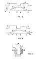
- Fig. 1 in schematischer Darstellung eine Anordnung zur Durchführung des erfindungsgemäßen Verfahrens zum Ausrichten und Prüfen von mit Mustern versehenen Werkstücken,
- Fig. 2 eine Gesamtansicht eines zu prüfenden Werkstücks in Draufsicht,
- Fig. 3 in vergrößerter Darstellung ein bestimmtes Feld des Werkstücks gemäß Fig. 2,
- Fig. 4 ein schematisches Schaltbild der in der Anordnung nach Fig. 1 verwendeten Bemessungsschaltung,
- Fig. 5 ein schematisches Schaltbild der in der Anordnung nach Fig. 1 verwendeten Schwellwertschaltung,
- Fig. 6 einen Teilbereich des in Fig. 3 dargestellten Feldes in der Verwendung für das Ausrichten,
- Fig. 7 den Teilbereich gemäß Fig. 6 mit Darstellung der bei der Fehlerprüfung verwendeten Randbereiche an den Grenzen der Muster- und der ungemusterten Flächen,
- Fig. 8 ein Diagramm mit den Eingangs- und Ausgangssignalen der Bemessungsschaltung gemäß Fig. 4 während eines Abtastvorganges,
- Fig. 9 ein Diagramm entsprechend der Fig. 8, jedoch für die Abtastung eines Musters gemäß Fig. 10 und
- Fig. 10 die Darstellung eines Musters mit verschobenen, asymmetrischen Abtastbereichen.
- 1 shows a schematic representation of an arrangement for carrying out the method according to the invention for aligning and testing workpieces provided with patterns,
- 2 is an overall view of a workpiece to be tested in plan view,
- 3 an enlarged view of a specific field of the workpiece according to FIG. 2,
- 4 shows a schematic circuit diagram of the rated circuit used in the arrangement according to FIG. 1,
- 5 is a schematic circuit diagram of the threshold circuit used in the arrangement according to FIG. 1,
- 6 shows a partial area of the field shown in FIG. 3 in use for the alignment,
- 7 shows the partial area according to FIG. 6 with illustration of the edge areas used in the error check at the borders of the pattern and the unpatterned areas,
- Fig. 8 is a diagram with the input and output signals of the rated circuit 4 during a scanning process,
- FIG. 9 shows a diagram corresponding to FIG. 8, but for the scanning of a pattern according to FIGS. 10 and
- 10 shows the representation of a pattern with shifted, asymmetrical scanning areas.
Die in Fig. 1 dargestellte Anordnung enthält einen in X- und Y-Richtung verstellbaren Tisch 10, auf dem das zu prüfende Werkstück 11, z.B. eine Maske, aufliegt. Das Werkstück 11 besteht, wie Fig. 2 zeigt, aus einem Substrat 12 mit einer Anzahl Grob-Richtmarken 13a, 13b, 13c und 13d sowie einer Anzahl Felder 14. Die Grob-Richtmarken 13 sind als Kreuze ausgebildet, können aber auch in Form eines Winkels usw. dargestellt sein.The arrangement shown in Fig. 1 includes a table 10 adjustable in the X and Y directions, on which the workpiece 11 to be tested, e.g. a mask. As shown in FIG. 2, the workpiece 11 consists of a
Als Werkstücke kommen im vorliegenden Zusammenhang auch als Chipträger verwendete gemusterte Substrate in Betracht oder optisch durchlässige Masken aus Glas mit einer Schicht optisch undurchlässiger Materialien, wie Metall oder Photoresist. Andererseits können die Masken auch aus anderen Materialien, wie z.B. Silicon, bestehen, die für infrarotes Licht durchlässig sind. Im vorliegenden Beispiel wird ein Substrat 12 aus Glas zugrundegelegt, dessen Muster 15 durch auf das Glas aufgetragene dünne Metallfilme gebildet ist..In the present context, workpieces that are used as chip carriers or optically transparent masks made of glass with a layer of optically opaque materials, such as metal or photoresist, are also considered as workpieces. On the other hand, the masks can also be made of other materials, e.g. Silicon exist, which are transparent to infrared light. In the present example, a
Jedes Feld besteht, wie Fig. 3 zeigt, aus einer Anzahl unterschiedlicher geometrischer metallisierter Muster 15, die, wie erwähnt, auf das Substrat 12 aufgetragen sind. üblicherweise, wenn auch nicht in jedem Fall, sind die Felder 14 untereinander identisch. Die nachfolgend beschriebene Ausrichtung und Prüfung der einzelnen Felder setzt dies jedoch nicht voraus. Jede zu prüfende Maske kann daher eine Vielzahl unterschiedlicher Muster einschließlich der Steuertestmuster aufweisen.As shown in FIG. 3, each field consists of a number of different geometric
Die Anordnung gemäß Fig. 1 enthält weiterhin ein Elektronenstrahlgerät 16, eine Strahlsteuerung 17, einen Detektor 18, einen Verstärker 19, eine Schwellwertschaltung 20, einen Vergleicher 21, eine Bemessungsschaltung 22, eine Muster-Halte-Schaltung 23, eine Digitalsteuerung 24 sowie einen Schalter 25 zum Verbinden des Detektors 18 und des Verstärkers 19 entweder mit dem Vergleicher 21, der Schwellwertschaltung 20 oder der Bemessungsschaltung 22. Dabei ist die Betätigung des Schalters 25 mittels einer Leitung 17a mit den Operationen der Strahlsteuerung 17 synchronisiert. Die Digitalsteuerung 24 ist als Universalrechner (Prozessor) ausgebildet und enthält alle erforderlichen Informationen und Daten bezüglich der zu prüfenden Maske einschließlich aller Richtmarken sowie der Form und Position der einzelnen Muster 15. Weiterhin erzeugt die Digitalsteuerung 24 die Signale zum Betrieb der Strahlsteuerung 17, die über eine Leitung 26 die Elektronenstrahlquelle 27 zur Erzeugung des Elektronenstrahls 28 ein- und ausschaltet. Die Strahlsteuerung 17 steuert weiterhin über die Leitungen 29 und 30 in bekannter Weise die Ablenkplatten 31 und 32 für den Elektronenstrahl 28 und synchronisiert über die Leitungen 17a und 17b die Operationen der Schwellwertschaltung 20, des Vergleichers 21, der Bemessungsschaltung 22 und der Muster-Halte-Schaltung 23 sowie des Schalters 25. Schließlich steuert die Digitalsteuerung 24 über eine Leitung 33 auch die jeweilige Position des Tisches 10.1 further includes an
Die zu prüfende Maske wird auf dem Tisch 10 durch eine entsprechende Spannvorrichtung, beispielsweise mittels Vakuum, festgehalten. Bei der dargestellten Ausführung ist auf der Oberfläche des Substrats 12 eine dünne, leitende, geerdete transparente Schicht 53 aufgebracht, wodurch sichergestellt ist, daß der Elektronenstrahl weder das die Muster 15a, 15b usw. bildende Material noch das Substrat selbst auflädt, während er über die ausgewählten Bereiche geführt wird. Ein geeignetes Material hierfür ist beispielsweise Zinnoxid. Die Schicht 53 (Fig. 2) ist jedoch nicht erforderlich, wenn das Substrat leitend oder halbleitend ist, oder wenn es sich um einen Strahl ohne Aufladungseffekt handelt, wie z.B. einen Lichtstrahl.The mask to be tested is held on the table 10 by an appropriate clamping device, for example by means of a vacuum. In the illustrated embodiment, a thin, conductive, grounded,
Zunächst wird der Schalter 25 so eingestellt, daß der Detektor 18 und der Verstärker 19 über die Leitung 25b mit der Schwellwertschaltung 20 verbunden werden sowie die als Prozessor wirksame Digitalsteuerung 24 die Strahlsteuerung 17 zum Einschalten des Elektronenstrahls 28 veranlaßt, der die Maske 11 mit ihren Feldern 14 zu erfassen vermag. Das Auftreffen des Elektronenstrahls auf dem Glas des Substrats 12 und den unterschiedlichen Mustern 15 auf dem Substrat 12 verursacht sowohl Sekundärelektronen als auch von der Maske reflektierte rückstreuende Elektronen. Jedes der Materialien, wie z.B. Glas oder das die Muster bildende Material, emittiert unterschiedliche Stärken von Sekundärelektronen und rückstreuenden Elektronen.First of all, the
Aus dem vorgenannten Grund wird das Glas des Substrats 12 Sekundärelektronen von einer bestimmten, üblicherweise geringen Stärke emittieren, während die Muster Sekundärelektronen von hiervon abweichender, vorzugsweise höherer Stärke emittieren. Zur Vereinfachung wird daher im folgenden bei den beschriebenen Vorgängen die Ermittlung der jeweiligen Sekundärelektronen zugrundegelegt, obwohl die dargestellte Anordnung genauso rückstreuende Elektronen verwenden könnte.For the aforementioned reason, the glass of the
Der Elektronenstrahl wird nun zum Abtasten über ein ausgewähltes Feld 14 gesteuert. Hierbei entstehen unterschiedliche Stärken von Sekundärelektronen, je nachdem, ob der Strahl auf eine Glas- oder eine Musterfläche auftrifft. Diese Sekundärelektronen werden durch den Detektor 18 festgestellt, der ein entsprechendes Signal proportional zur jeweiligen Zahl der Sekundärelektronen erzeugt, welches durch den Verstärker 19 verstärkt und anschließend zur Schwellwertschaltung 20 übertragen wird. Die Schwellwertschaltung 20 enthält, wie Fig. 5 zeigt, ein Paar von Muster-Halte-Schaltungen 34 und 35 sowie einen Spannungsteiler 36.The electron beam is now controlled for scanning over a selected
Der Elektronenstrahl wird zunächst auf die Glasfläche des Substrats 12 gerichtet, und gleichzeitig sendet die Digitalsteuerung 24 über eine Leitung 37 ein Signal zur Muster-Halte-Schaltung 34 zu deren Einschaltung, und dieses Signal endet nach einer vorbestimmten Zeit. Sodann wird der Elektronenstrahl auf eine Musterfläche gerichtet, und ein zweites Signal gelangt über eine Leitung 38 zur Muster-Halte-Schaltung 35. Diese Maßnahmen dienen zur Bemessung des Schwellwerts in der Schaltung 20 für ein bestimmtes Feld der Maske.The electron beam is first directed onto the glass surface of the
Die Ausgangssignale der Muster-Halte-Schaltungen 34 und 35 gelangen über Leitungen 39 bzw. 40 zum Spannungsteiler 36, dessen Ausgangssignale über eine Leitung 41 dem Vergleicher 21 zugeführt werden und der eine Schwellwertspannung gegen die auf der Leitung 25a dem Vergleicher 21 zugeführten Signale liefert. Dieser Schwellwert ist daher dynamisch und wird durch den Durchschnittswert der unterschiedlichen Signalstärken bestimmt, wie sie bei der Abtastung der Sekundärelektronen von den Glasflächen und den Musterflächen entstehen. Diese Bestimmung eines Schwellwerts für die Signalstärke ist insbesondere von Wichtigkeit, wenn das aufgrund der Sekundärelektronen ermittelte Signal unruhig oder uneinheitlich ist, nämlich infolge von Dichteänderungen, geometrischen Fehlern oder ähnlichem schwankt. Für bestimmte Anwendungen kann man auch mehr als einen Schwellwert verwenden. Auch kann man den Schwellwert periodisch an wechselnde Strahlströme oder Signalstärken anpassen, wie sie durch unterschiedliche bestrahlte Objekte, wie Musterdicke oder -dichte verursacht sein können.The output signals of the sample and hold
Die Anordnung gemäß Fig. 1 kann, wenn erwünscht, mit einem optischen Mikroskop ausgerüstet werden, um das Werkstück 11 mittels visueller Beobachtung der Richtmarken 13a, 13b, 13c und 13d grob auszurichten. Im Anschluß daran wird die in der Digitalsteuerung 24 gespeicherte Information zur Einschaltung des Elektronenstrahlgeräts 16 und zur Steuerung der Bewegung des Tisches 10 eingesetzt. Hierbei wird das Werkstück, im folgenden als Maske 11 bezeichnet, um einen festgelegten Betrag und in eine vorgegebene Richtung bewegt, so daß der Strahl nun auf ein ausgewähltes Feld 14 gerichtet ist. Nun bewirkt die Strahlsteuerung 17, daß der Strahl 28 das ausgewählte Feld 14 bzw. einen bestimmten Bereich desselben überstreicht.If desired, the arrangement according to FIG. 1 can be equipped with an optical microscope in order to roughly align the workpiece 11 by means of visual observation of the alignment marks 13a, 13b, 13c and 13d. The information stored in the
Die genaue Registrierung jedes Feldes bis zu einer endgültigen vorbestimmten Prüfposition erhält man nun durch Abtasten bestimmter Muster 15 eines Bereichs oder Teilbereichs des ausgewählten Feldes 14. Dabei kann der ausgewählte Bereich ausschließlich zum Zweck des Ausrichtens und von Feld zu Feld gleich gestaltet sein, oder er ist ein Bestandteil des Feldmusters selbst, in welchem Fall das Muster von Feld zu Feld unterschiedlich sein kann. Die zum Zwecke der Registrierung abzutastenden Muster werden in der gleichen Weise vorbestimmt wie die entsprechenden Muster, die zur Durchführung der Prüfung benützt werden, wobei irgendein ausgewählter Bereich des Feldes verwendet werden kann. Ein Beispiel hierfür zeigt Fig. 6, wo drei im oberen linken Eckbereich des Feldes 14 angeordnete Musterbereiche gemäß Fig. 3 vergrößert dargestellt sind und als ausgewählter Bereich dieses Feldes im nachfolgenden Beispiel verwendet werden.The exact registration of each field up to a final predetermined test position can now be obtained by scanning
Es wird nun der Schalter 25 so eingestellt, daß die Bemessungsschaltung 22 über die Leitung 25c mit dem Detektor 18 und dem Verstärker 19 verbunden wird. Die Digitalsteuerung 24 bewirkt nun über die Strahlsteuerung 17 die Steuerung des Elektronenstrahls 28 derart, daß dieser ausgewählte Kanten jedes der Muster 15a, 15b und 15c abtastet und hierbei deren Lage relativ zu der gewünschten Prüfposition ermittelt. Ist die tatsächliche Position dieser ausgewählten Muster bestimmt, bewirkt die Bemessungsschaltung 22 über die Muster-Halte-Schaltung 23 und die Leitung 23a eine Positionskorrektur in der Strahlsteuerung 17, in deren Folge der Elektronenstrahl 28 in eine solche Lage gelenkt wird, daß in bezug auf den Bewegungsbereich des Strahls das gesamte ausgewählte Feld in die gewünschte Prüfposition gelangt.The
Läßt man den Strahl einen eine Kante des Muster überlappenden Bereich überstreichen und integriert das Signal, das hierbei längs der Kante des Musters entsteht, und kehrt man sodann die Signalpolarität um, so daß der Strahl eine entsprechende Länge der entgegengesetzten Kante des Musters überstreicht, und integriert man sodann dieses Signal und summiert die Integrationssignale auf, so erhält man einen Fehlerbetrag, der die Abweichung des Musterbildes von der gewünschten Prüfposition anzeigt, in die der ausgewählte Bereich des Feldes auszurichten ist. Dieser Fehlerbetrag ist unabhängig von eventuellen Größenfehlerwerten. In der beschriebenen Weise wird beispielsweise der Strahl zunächst auf die linke Kante, also in horizontaler Richtung über das Muster 15 geführt, die in Fig. 6 durch die schraffierte Fläche des Bereichs 44 dargestellt ist. Dieser Abtastvorgang erzeugt Sekundärelektronen sowohl vom Muster als auch von der Substratglasoberfläche, die vom Detektor 18 erkannt und der Bemessungsschaltung 22 zugeführt werden.Allowing the beam to sweep an area overlapping an edge of the pattern and integrating the signal that arises along the edge of the pattern and then reversing the signal polarity so that the beam sweeps a corresponding length of the opposite edge of the pattern and integrates one like that then this signal and adding up the integration signals, an error amount is obtained which indicates the deviation of the sample image from the desired test position into which the selected area of the field is to be aligned. This amount of error is independent of any size error values. In the manner described, for example, the beam is first guided to the left edge, that is to say in the horizontal direction, over the
Wie Fig. 4 zeigt, enthält die Bemessungsschaltung 22 eine Umkehrschaltung 50, eine Integrationsschaltung 51 und einen Schalter 52, der über die Leitung 22b von der Digitalsteuerung 24 betätigt wird. Durch Schließen des Schalters 52 wird die Umkehrschaltung 50 von der Bemessungsschaltung 52 getrennt.As shown in FIG. 4, the
Vor dem Abtasten des Bereichs 44 wird der Schalter 52 geöffnet, so daß das Signal durch die Umkehrschaltung 50 hindurchgelangt. Der Elektronenstrahl wird nun längs der Kante des Musters 15a bewegt. Die hierbei überstrichene Fläche habe eine bestimmte Breite B und Länge L und ist als den Bereich 44 darstellende schraffierte Fläche gezeichnet. Das hierbei abgetastete Signal wird vom Detektor 18 über die Leitung'25c zur Bemessungsschaltung 22 geleitet, die Umkehrschaltung kehrt das Eingangssignal um und führt es dem Integrator 51 zu, dessen Ausgangssignal auf Leitung 22a der Muster-Halte-Schaltung 23 zugeführt wird.Before the
Wie Fig. 8 zeigt, erzeugt der Detektor 18 zur Übertragung über die Leitung 25c einen Rechteckspannungsimpuls 85 von der Zeit t1 bis zur Zeit t2. Dieser Rechteckspannungsimpuls wird mittels der Bemessungsschaltung 22 in eine Spannungslinie mit zunehmendem Spannungswert umgewandelt, und dieses Signal erscheint auf Leitung 22a. Es beginnt zur Zeit t1 und wird kontinuierlich über einen Grundwert 80 (vgl. Fig. 8) erhöht, bis der Rechteckspannungsimpuls 85 zur Zeit t1 endet. Die Höhe h, um die die Spannungslinie 86 ansteigt, ist proportional zur Gesamtzahl der Sekundärelektronen, die von dem abgetasteten Bereich 44 emittiert werden. Ein Prozentsatz der Sekundärelektronen, die vom Detektor 18 festgestellt werden, stammt von der Substratglasoberfläche und der Rst von der Musteroberfläche.As shown in FIG. 8, the
Nach vollständiger Abtastung des Bereichs 44 wird der Elektronenstrahl 28 abgeschaltet, und die Bemessungsschaltung 22 wird durch Umschalten des Schalters 52 zurückgestellt. Nun wird der Strahl um einen der Breite des Musters 15a entsprechenden Betrag nach rechts geschwenkt, so daß nun der Bereich 45 längs der rechten Kante des Musters 15 überstrichen werden kann. Dieser Bereich 45 hat gleichfalls die Breite B und die Länge L. Bei der Abtastung dieses Bereichs werden in gleicher Weise die Sekundärelektronen durch den Detektor 18 registriert und von der Zeit t3 bis zur Zeit t4 als Rechteckspannungsimpuls 87 über die Leitung 25c zur Bemessungsschaltung 22 übertragen. Da jedoch in diesem Fall der Schalter 25 in der Stellung ist, in welcher die Umkehrschaltung 50 ausgeschaltet ist, wird dieses Signal unter Umgehung der Umkehrschaltung 50 unmittelbar dem Integrator 51 zugeführt. Das Ausgangssignal der Bemessungsschaltung 22 ist durch die Spannungslinie 88 mit abnehmendem Spannungswert charakterisiert. Wenn diese Spannungslinie, wie dargestellt, zur Zeit t4 den Grundwert 80 erreicht, zeigt dies, daß der Bereich 44 genau den gleichen Betrag des Musters 15a überlappt wie der Bereich 45.After complete scanning of the
Wenn die Abtastung nicht genau die gleichen Beträge für den Musterbereich und die Substratglasoberfläche der Schicht 53 ergibt, erhält man unterschiedliche Höhenwerte für die Spannungslinie 86 mit zunehmendem Spannungswert einerseits und die Spannungslinie 88 mit abnehmendem Spannungswert andererseits mit der Folge, daß die Spannungslinie 88 nicht bis auf den Grundwert 80 zurückkehrt. In diesem Fall kann der Differenzwert als Anzeige für den Korrekturwert gewertet werden, der zur Erreichung der gewünschten Prüfposition zu berücksichtigen ist. Dieser Fall wird im folgenden anhand der Fign. 9 und 10 erläutert.If the scan does not give exactly the same amounts for the pattern area and the substrate glass surface of the
In Fig. 10 sind das Muster 102 überlappende Abtastbereiche 100 und 101 gezeigt, wobei der Abtastbereich 100 das Muster 102 um einen größeren Betrag überschneidet als der Abtastbereich 101. Gemäß Fig. 9 ergibt die Abtastung des Bereichs 100 einen Rechteckspannungsimpuls von der Zeit t1 bis zur Zeit t2, welcher mittels der Bemessungsschaltung 22 in einer Spannungslinie 96 mit zunehmendem Spannungswert umgewandelt wird, beginnend am Grundwert 94. Da der Abtastbereich 100 eine größere Fläche des Musters 102 überdeckt, ist die Zahl der festgestellten Sekundärelektronen entsprechend höher.10, scan
Der Elektronenstrahl überstreicht nun anschließend den Abtastbereich 101, und in der Folge des geringeren Überlappungsbereich desselben ist der Rechteckspannungsimpuls 97 im Zeitintervall von t3 bis t4 von geringerer Höhe als der Rechteckspannungsimpuls 95. Infolgedessen erreicht die daraus resultierende Spannungslinie 98 mit abnehmendem Spannungswert nicht den Grundwert 94, sondern endet in einer mit 99 bezeichneten Höhe oberhalb des Grundwerts 94. Dieser Wert ist proportional zur Abweichung K der Kante des Musters 102 von der Zentrallinie der Abtaststrahlen, und dieser Abweichungswert wird nun über die Leitung 23a zur Strahlsteuerung 17 übertragen, um die Strahlrichtung entsprechend zu korrigieren. Wenn gewünscht, kann die erhaltene Information gleichzeitig zur Digitalsteuerung 24 übermittel werden, die ihrerseits entsprechende Steuersignale zur Strahlsteuerung 17 sendet.The electron beam then sweeps over the
Überstreicht man mit dem Elektronenstrahl zunächst die rechte und dann die linke Kante des Musters 15a und integriert man sodann die in beiden Fällen ermittelte Zahl der abgetasteten Sekundärelektronen, so kann die Position der Abtaststrahlen in bezug auf das Muster in der Richtung von links nach rechts bestimmt werden. Wenn gewünscht, kann dieses Verfahren unter Zugrundelegung eines anderen linken Bereichs 46 des Musters 15c und eines rechten Bereichs 47 des Musters 15b wiederholt werden. Ist der betreffende Bereich, als Teil des gesamten Feldes, in der Richtung von links nach rechts, also in horizontaler Richtung in die gewünschte Position justiert worden, so wird das gleiche Verfahren in bezug auf die Richtung von oben nach unten, also in vertikaler Richtung wiederholt. Hierzu wird der Elektronenstrahl zunächst über den Bereich 48 im oberen Teil des Musters 15a geführt und dann über den Bereich 49 im unteren Teil des Musters 15c, wie in Fig. 6 dargestellt. Auch in diesem Fall handelt es sich um Flächen mit gleicher Breite und Länge, so daß die resultierenden Signale proportional zum Betrag der Überlappung von Strahl und Mustern sind. Die hierbei ermittelte Information wird nun wiederum der Strahlsteuerung 17 zugeführt, um eine entsprechende Korrektur in der Vertikalrichtung zur Erreichung der gewünschten Prüfposition auszuführen.If the electron beam is first swept over the right and then the left edge of the
Nach Durchführung dieser Feldregistrierung kann nun das gesamte Feld geprüft werden. Hierzu wird zunächst der Schalter 25 zurückgeschaltet, so daß die Bemessungsschaltung 22 abgeschaltet und der Vergleicher 21 an den Detektor 18 und den Verstärker 19 angeschlossen wird. Nun wird ein Spannungswert entsprechend dem zuvor ermittelten Schwellwert von der Schwellwertschaltung 20 über die Leitung 41 dem Vergleicher 21 zugeführt. Die Digitalsteuerung 24, in der alle Daten über die zu prüfenden Muster enthalten sind, veranlaßt das Einschalten des Elektronenstrahls 28 zur Abtastung der Muster 15a, 15b und 15c innerhalb des zu prüfenden Bereichs. Hierbei ist der Strahl von einheitlicher Größe und wandert nur über diejenigen Flächen der Bereiche, in denen sich Muster befinden. Der Vergleicher 21 liefert für den jeweiligen Sekundärelektronenstrom von jedem abgetasteten Muster ein Signal zur Digitalsteuerung 24, sooft das Abtastsignal unter die Schwellwertspannung abfällt, wobei die entsprechenden Koordinaten des Strahls zur Anzeige "fehlendes Muster" an dieser Stelle registriert werden. Wenn jedes der Muster 15a, 15b und 15c abgetastet ist, wird der Strahl schrittweise weitergeschaltet über diejenigen Bereiche, wo keine Muster oder musterartige Materialien zu erwarten sind. Auch hierbei wird der Sekundärelektronenstrom gemessen und der Digitalsteuerung 24 immer dann ein Signal zugeführt, wenn der Strom den festgelegten Schwellwert überschreitet. In diesem Fall werden die entsprechenden Koordinatenwerte des Strahls gleichfalls registriert, zur Anzeige, daß an dieser Stelle ein Muster oder ein musterähnliches Material festgestellt wurde, obwohl hier keines erwartet worden ist.After performing this field registration, the entire field can now be checked. For this purpose, the
Wie in Fig. 7 dargestellt, ist es erwünscht, daß ein schmaler Randbereich um die Muster 15a, 15b und 15c herum bei der Abtastung durch den Elektronenstrahl ausgespart wird. Dieser Randbereich 150 ist in Fig.7 durch die gestrichelten Linien 151 und 152 (Muster 15a) dargestellt. Demgemäß erfolgt die Abtastung des Musters 15a über dem Bereich der schraffierten Fläche innerhalb der gestrichelten Linie 151 und die Abtastung der umgebenden Bereiche außerhalb der gestrichelten Linie 152. Entsprechendes gilt für die Muster 15b und 15c. Selbstverständlich ist, wenn man auf diese Randbereiche 150 verzichtet, der Schaltungs- und Programmspeicheraufwand erheblich gering.As shown in Fig. 7, it is desirable that a narrow edge area around the
Jeder einen Teilbereich eines Feldes bildende Bereich wird aufeinanderfolgend dreimal abgetastet: Das erste Mal mit einer Ablenkung über die Kanten der erwarteten Muster in dem betreffenden Bereich, um die Lage des betreffenden Bereichs unmittelbar zu registrieren; das zweite Mal mit einer Ablenkung über alle Teile des betreffenden Bereichs, von denen eine bestimmte Signalstärke erwartet wird, und das dritte Mal mit einer Ablenkung des Strahls über alle anderen Teile des Bereichs, von denen die andere Signalstärke erwartet wird. Die beiden letzten Abtastvorgänge sind daher im wesentlichen komplementär innerhalb eines Bereichs, jedoch von einem Bereich zum nächsten unterschiedlich. Alle drei Abtastvorgänge sind jeweils durch die vorliegende gespeicherte Information über die bestehenden Muster auf dem zu prüfenden Werkstück definiert, wobei üblicherweise die numerischen Datentafeln verwendet werden, die bereits zur Herstellung des Werkstücks dienten. Das Abtasten der zuvor beschriebenen komplementären Bereiche wird zweckmäßig durch die Abtastung aufeinanderfolgender einzelner Rechteckbereiche durchgeführt, mit vorgegebenen Koordinaten für jede Strahlposition, so daß bei Abweichung von einem erwarteten Reflexionssignal die Koordinaten der betreffenden Fehlerposition unmittelbar zur Verfügung stehen und für eine nachfolgende Reparatur registriert werden können. Die Anwendung von rechteckigen oder quadratischen, nicht überlappenden Strahlbereichen ist bekannt. Die Verwendung relativ großer überlappender rechteckiger Strahlbereiche hat demgegenüber die Vorteile eines höheren Durchsatzes, höherer Sicherheit in der Feststellung signifikanter Fehlstellen, geringere Wahrscheinlichkeit der irrtümlichen Identifizierung von Fehlstellen sowie ausreicher Signalstärke.Each area forming a partial area of a field is scanned three times in succession: the first time with a deflection over the edges of the expected patterns in the area in question in order to immediately register the position of the area in question; the second time with a deflection over all parts of the area in question from which a certain signal strength is expected, and the third time with a deflection of the beam over all other parts of the area from which the other signal strength is expected. The last two scans are therefore essentially complementary within one area, but differ from one area to the next. All three scanning processes are each defined by the stored information about the existing patterns on the workpiece to be tested, usually using the numerical data tables that were already used to manufacture the workpiece. The scanning of the complementary areas described above is expediently carried out by scanning successive individual rectangular areas, with predetermined coordinates for each beam position, so that in the event of a deviation from an expected reflection signal, the coordinates of the relevant error position are immediately available and can be registered for a subsequent repair. The use of rectangular or square, non-overlapping beam areas is known. In contrast, the use of relatively large overlapping rectangular beam areas has the advantages of higher throughput, greater certainty in the detection of significant defects, less likelihood of erroneous identification of defects and sufficient signal strength.
Claims (10)
dadurch gekennzeichnet,
characterized,
dadurch gekennzeichnet,
characterized,
dadurch gekennzeichnet,
characterized,
dadurch gekennzeichnet,
characterized,
dadurch gekennzeichnet,
characterized,
dadurch gekennzeichnet,
daß als Abtaststrahl ein Elektronenstrahl verwendet wird.6. The method according to claims 1 to 5,
characterized,
that an electron beam is used as the scanning beam.
dadurch gekennzeichnet,
daß als Abtaststrahl ein Kathodenstrahl verwendet wird.7. The method according to claims 1 to 5,
characterized,
that a cathode beam is used as the scanning beam.
daß als Abtaststrahl ein optischer Strahl verwendet wird.8. The method according to claims 1 to 5, characterized in
that an optical beam is used as the scanning beam.
dadurch gekennzeichnet,
daß das Substrat aus Silicium besteht und der Abtaststrahl durch infrarotes Licht gebildet wird.9. The method according to claims 1 to 5 and 8,
characterized,
that the substrate is made of silicon and the scanning beam is formed by infrared light.
dadurch gekennzeichnet,
daß das Werkstück als Substrat aus transparentem Werkstoff ausgebildet ist und das Muster als darauf aufgetragene, für den Abtaststrahl nicht transparente Filmschicht ausgebildet ist, derart, daß die Oberflächen von Werkstück und Muster unterschiedliche Reflektienswerte für den Strahl aufweisen.10. The method according to claims 1 to 5, 6, 7 or 8,
characterized,
that the workpiece is designed as a substrate made of transparent material and the pattern is designed as a film layer applied thereon, which is not transparent to the scanning beam, such that the surfaces of the workpiece and pattern have different reflectance values for the beam.
Applications Claiming Priority (4)
| Application Number | Priority Date | Filing Date | Title |
|---|---|---|---|
| US06/218,323 US4365163A (en) | 1980-12-19 | 1980-12-19 | Pattern inspection tool - method and apparatus |
| US06/218,322 US4357540A (en) | 1980-12-19 | 1980-12-19 | Semiconductor device array mask inspection method and apparatus |
| US218322 | 1980-12-19 | ||
| US218323 | 1998-12-22 |
Publications (2)
| Publication Number | Publication Date |
|---|---|
| EP0054710A1 true EP0054710A1 (en) | 1982-06-30 |
| EP0054710B1 EP0054710B1 (en) | 1986-02-05 |
Family
ID=26912798
Family Applications (1)
| Application Number | Title | Priority Date | Filing Date |
|---|---|---|---|
| EP19810109166 Expired EP0054710B1 (en) | 1980-12-19 | 1981-10-29 | Positioning and controlling procedure of a workpiece provided with patterns, for example of a mask for manufacturing semi-conductor elements |
Country Status (2)
| Country | Link |
|---|---|
| EP (1) | EP0054710B1 (en) |
| DE (1) | DE3173738D1 (en) |
Cited By (3)
| Publication number | Priority date | Publication date | Assignee | Title |
|---|---|---|---|---|
| EP0130497A2 (en) * | 1983-06-30 | 1985-01-09 | International Business Machines Corporation | Alignment technique for a scanning beam |
| EP0155687A2 (en) * | 1984-03-23 | 1985-09-25 | International Business Machines Corporation | Method of forming inspection patterns |
| EP0177717A1 (en) * | 1984-09-04 | 1986-04-16 | Siemens Aktiengesellschaft | Process for the automatic positioning of a curpuscular probe |
Citations (3)
| Publication number | Priority date | Publication date | Assignee | Title |
|---|---|---|---|---|
| US3901814A (en) * | 1974-06-27 | 1975-08-26 | Ibm | Method and apparatus for detecting a registration mark on a target such as a semiconductor wafer |
| FR2439437A1 (en) * | 1978-10-16 | 1980-05-16 | Nippon Telegraph & Telephone | PROCESS AND DEVICE FOR EXAMINING PATTERNS SUCH AS THOSE MASKS USED IN THE MANUFACTURE OF INTEGRATED CIRCUITS |
| US4264822A (en) * | 1978-11-27 | 1981-04-28 | Hitachi, Ltd. | Electron beam testing method and apparatus of mask |
-
1981
- 1981-10-29 EP EP19810109166 patent/EP0054710B1/en not_active Expired
- 1981-10-29 DE DE8181109166T patent/DE3173738D1/en not_active Expired
Patent Citations (3)
| Publication number | Priority date | Publication date | Assignee | Title |
|---|---|---|---|---|
| US3901814A (en) * | 1974-06-27 | 1975-08-26 | Ibm | Method and apparatus for detecting a registration mark on a target such as a semiconductor wafer |
| FR2439437A1 (en) * | 1978-10-16 | 1980-05-16 | Nippon Telegraph & Telephone | PROCESS AND DEVICE FOR EXAMINING PATTERNS SUCH AS THOSE MASKS USED IN THE MANUFACTURE OF INTEGRATED CIRCUITS |
| US4264822A (en) * | 1978-11-27 | 1981-04-28 | Hitachi, Ltd. | Electron beam testing method and apparatus of mask |
Non-Patent Citations (2)
| Title |
|---|
| IBM Technical Disclosure Bulletin, Band II, Heft 12, Mai 1969, New York (US) R.F. TYNAN: "Integrated Circuitmask Inspection Technique", seiten 1695-1696 *ingesamt* * |
| IEEE Transactions on Electron Devices, Band ED-27, Heft 8, August 1980, New York(US) YASUO TARUI: "Basic Technology for VLSI (Part II)", seiten 1321-1331 *figuren 8 und 10; Absatz III "Electron Beam Mask Inspection" auf seiten 1322 bis 1324* * |
Cited By (5)
| Publication number | Priority date | Publication date | Assignee | Title |
|---|---|---|---|---|
| EP0130497A2 (en) * | 1983-06-30 | 1985-01-09 | International Business Machines Corporation | Alignment technique for a scanning beam |
| EP0130497A3 (en) * | 1983-06-30 | 1985-03-13 | International Business Machines Corporation | Alignment technique for a scanning beam |
| EP0155687A2 (en) * | 1984-03-23 | 1985-09-25 | International Business Machines Corporation | Method of forming inspection patterns |
| EP0155687A3 (en) * | 1984-03-23 | 1987-12-16 | International Business Machines Corporation | Method of forming inspection patterns |
| EP0177717A1 (en) * | 1984-09-04 | 1986-04-16 | Siemens Aktiengesellschaft | Process for the automatic positioning of a curpuscular probe |
Also Published As
| Publication number | Publication date |
|---|---|
| EP0054710B1 (en) | 1986-02-05 |
| DE3173738D1 (en) | 1986-03-20 |
Similar Documents
| Publication | Publication Date | Title |
|---|---|---|
| DE2222665A1 (en) | Method and apparatus for aligning electron projection systems | |
| DE19825829C2 (en) | Method for determining the distance P of an edge of a structural element on a substrate | |
| DE2810025A1 (en) | DEVICE FOR MEASURING THE INCLINATION OF A SURFACE | |
| DE2939044A1 (en) | DEVICE FOR ELECTRON BEAM LITHOGRAPHY | |
| EP0043863A1 (en) | Process for compensating the proximity effect in electron beam projection devices | |
| DE10047211A1 (en) | Method and measuring device for determining the position of an edge of a structural element on a substrate | |
| DE102007042271B3 (en) | Methods for determining position of stripping edge of disk-shaped object, involves recording boundary region of object in line-by-line manner, where boundary region has stripping edge | |
| DE2260229C3 (en) | ||
| DE4221080C2 (en) | Structure and method for direct calibration of alignment measuring systems for specific semiconductor wafer process topography | |
| EP0003038B1 (en) | Method for overlay measurement using an electronic beam system as a measuring tool | |
| DE3206374C2 (en) | Method and apparatus for calibrating the deflection of a beam composed of charged particles | |
| DE19802848B4 (en) | Method and apparatus for testing a substrate | |
| DE102007039982B3 (en) | Method for optical inspection and visualization of the optical knife values obtained from disc-shaped objects | |
| DE1804646A1 (en) | Corpuscular beam processing device with an object table and deflection means for the beam | |
| DE3410885A1 (en) | ERROR-CORRECTED ROD LITHOGRAPHY | |
| DE19732668A1 (en) | Light calibrating procedure for laser beam scanning device | |
| DE2905635A1 (en) | METHOD AND DEVICE FOR ALIGNING THE IMAGE AND / OR OBJECT AREAS IN OPTICAL COPYING DEVICES | |
| EP0176745A1 (en) | Device and method to measure lengths in a scanning corpuscular microscope | |
| DE3226999A1 (en) | METHOD AND DEVICE FOR DETECTING ANOMALIES IN THE REPRODUCTION OF A PATTERN | |
| DE19817714B4 (en) | Method for measuring the position of structures on a mask surface | |
| EP0054710B1 (en) | Positioning and controlling procedure of a workpiece provided with patterns, for example of a mask for manufacturing semi-conductor elements | |
| DE3006379C2 (en) | ||
| DE2731142C3 (en) | Method for determining the position of an electron beam in relation to alignment marks arranged on an object and device for carrying out the method | |
| DE19544753A1 (en) | Electron beam lithographic appts. for semiconductor integrated circuit mfr. | |
| DE3744320C2 (en) |
Legal Events
| Date | Code | Title | Description |
|---|---|---|---|
| PUAI | Public reference made under article 153(3) epc to a published international application that has entered the european phase |
Free format text: ORIGINAL CODE: 0009012 |
|
| 17P | Request for examination filed |
Effective date: 19811029 |
|
| AK | Designated contracting states |
Designated state(s): DE FR GB |
|
| GRAA | (expected) grant |
Free format text: ORIGINAL CODE: 0009210 |
|
| AK | Designated contracting states |
Designated state(s): DE FR GB |
|
| ET | Fr: translation filed | ||
| REF | Corresponds to: |
Ref document number: 3173738 Country of ref document: DE Date of ref document: 19860320 |
|
| PLBE | No opposition filed within time limit |
Free format text: ORIGINAL CODE: 0009261 |
|
| STAA | Information on the status of an ep patent application or granted ep patent |
Free format text: STATUS: NO OPPOSITION FILED WITHIN TIME LIMIT |
|
| 26N | No opposition filed | ||
| PG25 | Lapsed in a contracting state [announced via postgrant information from national office to epo] |
Ref country code: GB Effective date: 19891029 |
|
| GBPC | Gb: european patent ceased through non-payment of renewal fee | ||
| PG25 | Lapsed in a contracting state [announced via postgrant information from national office to epo] |
Ref country code: FR Effective date: 19900629 |
|
| PG25 | Lapsed in a contracting state [announced via postgrant information from national office to epo] |
Ref country code: DE Effective date: 19900703 |
|
| REG | Reference to a national code |
Ref country code: FR Ref legal event code: ST |