EP0053545B1 - Système de transmission d'informations à modulation directe de la lumière à liaison optique à bande passante étendue vers les fréquences basses et le continu - Google Patents
Système de transmission d'informations à modulation directe de la lumière à liaison optique à bande passante étendue vers les fréquences basses et le continu Download PDFInfo
- Publication number
- EP0053545B1 EP0053545B1 EP81401842A EP81401842A EP0053545B1 EP 0053545 B1 EP0053545 B1 EP 0053545B1 EP 81401842 A EP81401842 A EP 81401842A EP 81401842 A EP81401842 A EP 81401842A EP 0053545 B1 EP0053545 B1 EP 0053545B1
- Authority
- EP
- European Patent Office
- Prior art keywords
- optical
- low
- diode
- photodiode
- transmission system
- Prior art date
- Legal status (The legal status is an assumption and is not a legal conclusion. Google has not performed a legal analysis and makes no representation as to the accuracy of the status listed.)
- Expired
Links
- 230000005540 biological transmission Effects 0.000 title claims abstract description 41
- 230000003287 optical effect Effects 0.000 claims abstract description 47
- 230000000694 effects Effects 0.000 claims abstract description 44
- 230000009021 linear effect Effects 0.000 claims abstract description 40
- 238000001914 filtration Methods 0.000 claims abstract description 9
- 238000006243 chemical reaction Methods 0.000 claims description 18
- 239000004020 conductor Substances 0.000 claims 1
- 230000007547 defect Effects 0.000 abstract description 2
- 230000035945 sensitivity Effects 0.000 abstract 1
- 238000010586 diagram Methods 0.000 description 11
- 230000014509 gene expression Effects 0.000 description 4
- 230000010287 polarization Effects 0.000 description 4
- 230000008901 benefit Effects 0.000 description 3
- 230000001419 dependent effect Effects 0.000 description 3
- 230000004044 response Effects 0.000 description 3
- 230000007423 decrease Effects 0.000 description 2
- 239000013307 optical fiber Substances 0.000 description 2
- 230000009471 action Effects 0.000 description 1
- 230000008859 change Effects 0.000 description 1
- 230000000295 complement effect Effects 0.000 description 1
- 230000003247 decreasing effect Effects 0.000 description 1
- 230000004907 flux Effects 0.000 description 1
- 238000002955 isolation Methods 0.000 description 1
- 238000012986 modification Methods 0.000 description 1
- 230000004048 modification Effects 0.000 description 1
- 230000009022 nonlinear effect Effects 0.000 description 1
- 238000011084 recovery Methods 0.000 description 1
- 230000009466 transformation Effects 0.000 description 1
- 230000003313 weakening effect Effects 0.000 description 1
Images


Classifications
-
- H—ELECTRICITY
- H04—ELECTRIC COMMUNICATION TECHNIQUE
- H04B—TRANSMISSION
- H04B1/00—Details of transmission systems, not covered by a single one of groups H04B3/00 - H04B13/00; Details of transmission systems not characterised by the medium used for transmission
- H04B1/62—Details of transmission systems, not covered by a single one of groups H04B3/00 - H04B13/00; Details of transmission systems not characterised by the medium used for transmission for providing a predistortion of the signal in the transmitter and corresponding correction in the receiver, e.g. for improving the signal/noise ratio
-
- H—ELECTRICITY
- H04—ELECTRIC COMMUNICATION TECHNIQUE
- H04B—TRANSMISSION
- H04B10/00—Transmission systems employing electromagnetic waves other than radio-waves, e.g. infrared, visible or ultraviolet light, or employing corpuscular radiation, e.g. quantum communication
- H04B10/50—Transmitters
- H04B10/501—Structural aspects
- H04B10/502—LED transmitters
Definitions
- the present invention relates to an information transmission system with direct light modulation with an optical link and more particularly with an optical link whose bandwidth is sought to extend towards low frequencies and the continuous.
- optical links have the advantage over electrical connections of galvanic isolation and a wide bandwidth, but the drawback of attenuation which can vary significantly during operation, variation in power transmission, variation in connector losses, variation in receiver efficiency.
- Direct modulation of the power produced by the transmission diode makes it possible to carry out a transmission whose bandwidth is identical to that of the useful signal. But on the other hand, because of a series of thermal phenomena appearing as much on the level of the emission as on the level of the reception, the transmission of the low frequencies and in particular of the zero frequency is done under bad conditions and faults such as attenuations, distortions, drifts appear.
- the object of the present invention is to eliminate these various defects while retaining the advantages of direct modulation which in particular allows a transmission whose occupied bandwidth is minimal.
- An object of the invention is to further increase the performance of the system by extending the bandwidth to low frequencies and the continuous, this also by providing it with means for compensating for the linear thermal effects produced by the emitting diode LED or and by the receiving laser when the latter is not of the PIN type, but of the avalanche type, known as APD.
- APD avalanche type
- a system for transmitting information with direct light modulation characterized in that it includes other filtering means to compensate for the linear thermal effects of the diodes, these complementary means being arranged at the reception and comprising a second low-pass filter determined to compensate for the linear thermal effects produced by the transmission diode for the low-frequency electrical signals delivered by the high-pass filter of the transmission means; in addition, if the photodiode is of the avalanche type, this second filter is itself followed by a third low-pass filter determined to compensate for the linear thermal effects produced by the photodiode for these same low-frequency signals.
- An optical link in a transmission system covered by the invention essentially consists, as shown in FIG. 1, of an optical transmitter 1 preceded in general by an amplifier 2, of the optical link proper 3 and of an optical receiver 4 followed by an amplifier 5.
- the emission diode can be of the LED or laser type.
- the receiving photodiode is of the PIN or avalanche type.
- the various emission diodes are essentially characterized by their power output function as a function of the injected current. For analog transmission, this characteristic should be as linear as possible.
- the different types of diodes mentioned have P-1 linear characteristics over the entire extent of the characteristic, this is the case with LED diodes or only on a part, this is the case with laser diodes. These characteristics are represented in FIG. 2a for an LED diode and in FIG. 2b for a laser diode.
- modulation of these diodes is carried out by polarizing the component using a quiescent current 10 and by superimposing on the latter an alternating modulation current varying the transmission power and constituting the signal.
- Figure 3a shows this modulation for an LED diode and Figure 3b for a laser diode.
- the receiving photodiodes whether of the PIN or avalanche type, perform the reverse transformation on arrival by delivering a current proportional to the power received
- This current creates a potential difference across a resistor and can then be amplified.
- the current-to-power conversion characteristic at the level of the transmitters and the power-to-current conversion characteristic at the level of avalanche diode receivers are highly dependent on the temperature of the junction. Therefore, the behavior of these components is very different depending on whether the modulating signal is at low or high frequency.
- This dependence generally results in a drop in the emitted power when the temperature increases for the emission diodes and a drop in the conversion slope g causing a drop in photocurrent for the avalanche photodiodes.
- FIGS. 4a and 4b illustrate respectively for an LED diode and a laser diode, the dependence of the power as a function of the temperature.
- FIG. 5 illustrates it, the evolution of the conversion slope of an avalanche photodiode as a function of the temperature.
- the components are sensitive to temperature. However, this dependence differs according to the speed of variation of the current on transmission or of the power on reception. Indeed, if the current modulating the emission diode or the optical power of the avalanche photodiode varies rapidly, the junction temperature of the component does not have time to vary and remains constant over time. On the other hand, if the frequency is very low, the junction heats up or cools depending on the instantaneous level of the signal, modifies the characteristics of the components and introduces a distortion of the signal. This deformation is all the more important the greater the modulation signal.
- a high-pass type filter 8 is placed before the transmitter, which limits the low frequencies to a low level and this up to a frequency beyond which the thermal phenomena no longer occur. , and on reception a low-pass filter 6 of reverse transfer function which perfectly restores the shape of the signal.
- Figure 6 gives the block diagram of a compensated chain for low frequencies.
- FIG. 6 is usable whatever the type of transmitter or receiver used, only the value of the cutoff frequencies of the filters being modified according to the case.
- an optical chain comprising an LED emission diode and a PIN type photodiode for reception.
- the emission diode is sensitive to temperature, the PIN photodiode having a constant response.
- the power emitted by an LED diode varies linearly ment with the current injected this for a given temperature of the junction.
- the temperature of the junction depends on the power dissipated in the diode, on the ambient temperature and on the thermal resistance between the junction and the case, and between the case and the room temperature.
- the electric power injected into the diode, Pe depends on the current flowing through the diode as well as on its voltage, the latter parameter being substantially independent of the current in the case of an LED or laser diode.
- the modulated power varies parabolically with the current and depends on the thermal resistance. There is therefore the appearance of a signal distortion, (this distortion disappears completely if the modulation frequency becomes high).
- the electrical signal used to modulate the LED is weakened, using a high-pass filter, and one returns to a modulator at low level at low frequency, and at normal level at high frequency.
- the correct signal is restored, using a reverse transfer function filter and placed after the receiving PIN photodiode.
- the linear effect due to the thermal impedance of the junction is corrected, using a low-pass filter placed at the reception.
- the two non-linear thermal effect correction filters 8 and 6 must have inverse transfer functions so that their effects compensate each other.
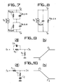
- FIGS. 9 give an example of a high pass filter 8 usable at transmission as well as its transfer function.
- This transfer function is: and the characteristic frequencies f1 and f2 of the filter are:
- the corresponding filter 6 which can be used on reception is shown in FIG. 10.
- the transfer function of this filter is and the characteristic frequencies are given by:
- This filter is of the same type as the previous one, only the component values differ.
- the frequencies f1 and f2 must be chosen to have the thermal cut-off frequency: sufficient attenuation of the low frequencies on transmission.
- the low frequencies of high level are weakened in the frequency zone of thermal phenomena by at least 20 dB and the signal returns to its normal level at from frequencies a hundred times higher than the thermal cutoff frequency f th which limits the non-linear thermal effect on these frequencies.
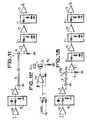
- FIG. 11 represents the complete diagram of the optical link compensated for the low frequencies. It will be noted and this is normal that this diagram resembles the diagram in FIG. 6, so that the references used will be the same.
- From the input E of the chain there is an amplifier 10, buffer followed by a filter 8, high-pass intended to correct the non-linear thermal effects of the emission LED 1, separated from the filter by an amplifier 2.
- the optical link 3 proper supplies a reception photodiode 4 of the PIN type followed by an amplifier 5, connected to the low-pass filter 6, responsible for correcting the non-linear thermal effects of the emission LED 1.
- a buffer amplifier 11 separates this filter 6 from the low-pass filter 7 responsible for correcting the linear thermal effects of the emission LED.
- the low-pass filter 7 for correcting the linear thermal effects due to the emission diode is shown in the case where the thermal impedance of the diode Zth is a thermal resistance shunted by a thermal capacity.
- this filter must have as transfer function the inverse of the transfer function due to the thermal effect, that is:
- the polarization device of the emission diode not shown in FIG. 11 can be, for example, a transistor 13 mounted as a variable current source and preceded by an operational amplifier 14 as shown in FIG. 12; we have
- the thermal model of the laser diode is identical to that of the LED diode and is reduced with the use of a radiator of low thermal resistance, to a thermal impedance made up of a thermal resistance in parallel with a thermal capacity:
- the transfer function recovery low pass filter is also identical to that used for the LED and is located after the PIN photodiode.
- the laser current is composed of a bias current io and a modulation current, that is:
- V D the laser voltage, constant and close to 2 volts.
- This transfer function (Pmod function of i) is that of a high-pass filter whose response curve is similar to that of the filter in Figure 9 and whose
- the transfer function is also of the same type as that encountered with the LED, and the compensation is done with a low-pass filter of the same type.
- the optical link with laser transmitter and PIN photodiode receiver therefore behaves identically to the chain using an LED emission diode.
- the diagram of this link is therefore identical to that of FIG. 11.
- the low-pass filter for correction of the linear thermal effects areas due to the emission diode must have as transfer function the inverse of the transfer function due to the thermal effect, that is:
- avalanche photodiodes are relatively temperature sensitive. The gain of these diodes decreases with the junction temperature and, therefore, the variation of the light flux striking the diode causes, for the low frequencies, a distortion comparable to that encountered at the LED or laser diode.
- junction-ambient thermal impedance can also be represented by a thermal resistance Rth shunted by a thermal capacity Cth:
- Tj - To is: T R with:
- the conversion slope for the modulated signal is:
- p is limited by the high-pass filter for correction on transmission, for high frequencies Zth - 0 and therefore p + Po no longer intervenes.
- thermal effect of the avalanche photodiode occurs at low level in the form of a high-pass transfer function identical to that encountered for LED or laser diodes.
- This linear action can be compensated with a low-pass filter of the same type as those already used for reception at the level of connections with PIN diode.
- the low-pass filter 7 of horn rection of the linear thermal effects due to the emission diode is represented figure 13 in the case where the thermal impedance of the emission diode Zth is a thermal resistance shunted by a thermal capacity.
- this filter must have as transfer function the inverse of the transfer function due to the thermal effect, ie: when the emission diode is an LED diode, when the diode is a laser diode.
- Zth ' represents the thermal impedance of the emission diode.
- the low-pass filter for correcting linear thermal effects due to the emission diode is also represented in FIG. 13 in the case where the thermal impedance Zth of the reception diode is a thermal resistance shunted by a thermal capacity.
- this filter must have as transfer function the inverse of the transfer function due to the thermal effect, ie:
- FIG. 13 represents the complete diagram of the compensated optical link when the emission diode being either an LED diode or a laser diode, the reception photodiode is an avalanche. It should be noted a priori that the diagram of the connection resembles that already represented in FIG. 6 and in FIG. 11 so that for identical or equivalent circuits the references used are the same. From input E, there is the amplifier 10 followed by the filter 8, a high pass correcting the non-linear thermal effects of the emission diode, of the amplifier 2 connected to the emission diode 1, of the Optical link proper 3, an optical fiber for example, which feeds the reception photodiode, of the avalanche type 40 with its load resistance R.
- This photodiode is connected to an amplifier 5 followed by the filter 6, low-pass intended to correct the non-linear thermal effects of the emission diode, connected to a buffer amplifier 11 followed by the filter 7 intended to correct the linear thermal effects of the emission diode.
- a buffer amplifier 12 connected to the output of the filter 7 is connected to the low-pass filter 9 intended to correct the linear thermal effects of the avalanche photodiode 40.
- a buffer amplifier 15, FIG. 13, connects the filter 9 to the output S of the link.
Landscapes
- Engineering & Computer Science (AREA)
- Computer Networks & Wireless Communication (AREA)
- Signal Processing (AREA)
- Physics & Mathematics (AREA)
- Electromagnetism (AREA)
- Optical Communication System (AREA)
Priority Applications (1)
| Application Number | Priority Date | Filing Date | Title |
|---|---|---|---|
| AT81401842T ATE8831T1 (de) | 1980-12-02 | 1981-11-20 | Nachrichtenuebertragungssystem mit direkter lichtmodulation, optischer verbindung und mit einer bandbreite, die sich zu tiefen frequenzen und zu gleichanteilen hin erstreckt. |
Applications Claiming Priority (2)
| Application Number | Priority Date | Filing Date | Title |
|---|---|---|---|
| FR8025560 | 1980-12-02 | ||
| FR8025560A FR2495412A1 (fr) | 1980-12-02 | 1980-12-02 | Systeme de transmission d'informations a modulation directe de la lumiere a liaison optique a bande passante etendue vers les frequences basses et le continu |
Publications (2)
| Publication Number | Publication Date |
|---|---|
| EP0053545A1 EP0053545A1 (fr) | 1982-06-09 |
| EP0053545B1 true EP0053545B1 (fr) | 1984-08-01 |
Family
ID=9248577
Family Applications (1)
| Application Number | Title | Priority Date | Filing Date |
|---|---|---|---|
| EP81401842A Expired EP0053545B1 (fr) | 1980-12-02 | 1981-11-20 | Système de transmission d'informations à modulation directe de la lumière à liaison optique à bande passante étendue vers les fréquences basses et le continu |
Country Status (6)
| Country | Link |
|---|---|
| US (1) | US4443890A (enExample) |
| EP (1) | EP0053545B1 (enExample) |
| JP (1) | JPS57119531A (enExample) |
| AT (1) | ATE8831T1 (enExample) |
| DE (1) | DE3165277D1 (enExample) |
| FR (1) | FR2495412A1 (enExample) |
Families Citing this family (30)
| Publication number | Priority date | Publication date | Assignee | Title |
|---|---|---|---|---|
| US4759080A (en) * | 1983-11-16 | 1988-07-19 | Nec Corporation | Coherent optical communication system with FSK heterodyne or homodyne detection and little influence by distortion of a modulated optical signal |
| DE3519711A1 (de) * | 1985-06-01 | 1986-12-04 | Hirschmann Radiotechnik | Schaltungsanordnung zur ansteuerung einer lichtemittierenden diode |
| SE8604792L (sv) * | 1986-11-07 | 1988-05-08 | Asea Atom Ab | Fiberoptisk dataoverforing vid borrhalslogging |
| US4989212A (en) * | 1990-04-09 | 1991-01-29 | Trw, Inc. | Laser diode phase modulation technique |
| ATE136705T1 (de) * | 1992-02-01 | 1996-04-15 | Sel Alcatel Ag | Digitales optisches nachrichtenübertragungssystem mit einem bei der betriebswellenlänge dispersionsbehafteten lichtwellenleiter |
| US5473017A (en) * | 1993-09-30 | 1995-12-05 | Exxon Chemical Patents Inc. | Intervulcanized elastomer blends |
| WO1996035972A1 (en) * | 1995-05-08 | 1996-11-14 | Testdesign Corporation | Optical fiber interface for integrated circuit test system |
| JPH11225435A (ja) * | 1997-11-10 | 1999-08-17 | Siliconix Inc | 赤外発光ダイオードを作動させるための方法及び回路 |
| US6963597B2 (en) * | 2000-04-28 | 2005-11-08 | Photodigm, Inc. | Grating-outcoupled surface-emitting lasers |
| US8835831B2 (en) | 2010-06-22 | 2014-09-16 | Zena Technologies, Inc. | Polarized light detecting device and fabrication methods of the same |
| US8519379B2 (en) | 2009-12-08 | 2013-08-27 | Zena Technologies, Inc. | Nanowire structured photodiode with a surrounding epitaxially grown P or N layer |
| US9478685B2 (en) | 2014-06-23 | 2016-10-25 | Zena Technologies, Inc. | Vertical pillar structured infrared detector and fabrication method for the same |
| US8269985B2 (en) | 2009-05-26 | 2012-09-18 | Zena Technologies, Inc. | Determination of optimal diameters for nanowires |
| US9299866B2 (en) | 2010-12-30 | 2016-03-29 | Zena Technologies, Inc. | Nanowire array based solar energy harvesting device |
| US9000353B2 (en) | 2010-06-22 | 2015-04-07 | President And Fellows Of Harvard College | Light absorption and filtering properties of vertically oriented semiconductor nano wires |
| US8748799B2 (en) | 2010-12-14 | 2014-06-10 | Zena Technologies, Inc. | Full color single pixel including doublet or quadruplet si nanowires for image sensors |
| US9082673B2 (en) | 2009-10-05 | 2015-07-14 | Zena Technologies, Inc. | Passivated upstanding nanostructures and methods of making the same |
| US8889455B2 (en) | 2009-12-08 | 2014-11-18 | Zena Technologies, Inc. | Manufacturing nanowire photo-detector grown on a back-side illuminated image sensor |
| US9515218B2 (en) | 2008-09-04 | 2016-12-06 | Zena Technologies, Inc. | Vertical pillar structured photovoltaic devices with mirrors and optical claddings |
| US9406709B2 (en) | 2010-06-22 | 2016-08-02 | President And Fellows Of Harvard College | Methods for fabricating and using nanowires |
| US8866065B2 (en) | 2010-12-13 | 2014-10-21 | Zena Technologies, Inc. | Nanowire arrays comprising fluorescent nanowires |
| US8791470B2 (en) * | 2009-10-05 | 2014-07-29 | Zena Technologies, Inc. | Nano structured LEDs |
| US8735797B2 (en) | 2009-12-08 | 2014-05-27 | Zena Technologies, Inc. | Nanowire photo-detector grown on a back-side illuminated image sensor |
| US8507840B2 (en) | 2010-12-21 | 2013-08-13 | Zena Technologies, Inc. | Vertically structured passive pixel arrays and methods for fabricating the same |
| US9343490B2 (en) | 2013-08-09 | 2016-05-17 | Zena Technologies, Inc. | Nanowire structured color filter arrays and fabrication method of the same |
| US8229255B2 (en) | 2008-09-04 | 2012-07-24 | Zena Technologies, Inc. | Optical waveguides in image sensors |
| US8546742B2 (en) | 2009-06-04 | 2013-10-01 | Zena Technologies, Inc. | Array of nanowires in a single cavity with anti-reflective coating on substrate |
| US8274039B2 (en) | 2008-11-13 | 2012-09-25 | Zena Technologies, Inc. | Vertical waveguides with various functionality on integrated circuits |
| US8299472B2 (en) | 2009-12-08 | 2012-10-30 | Young-June Yu | Active pixel sensor with nanowire structured photodetectors |
| US8890271B2 (en) | 2010-06-30 | 2014-11-18 | Zena Technologies, Inc. | Silicon nitride light pipes for image sensors |
Family Cites Families (5)
| Publication number | Priority date | Publication date | Assignee | Title |
|---|---|---|---|---|
| GB499317A (en) * | 1937-07-21 | 1939-01-23 | Standard Telephones Cables Ltd | Improvements in or relating to electric wave signalling systems |
| US3729633A (en) * | 1970-11-24 | 1973-04-24 | Ibm | Optical receiver having a maximized signal-to-noise ratio |
| US3984824A (en) * | 1975-07-25 | 1976-10-05 | The United States Of America As Represented By The Secretary Of The Army | Wide-band optical analog signal link using fiber optics |
| JPS5813038B2 (ja) * | 1976-09-13 | 1983-03-11 | 富士通株式会社 | Led変調方式 |
| US4257125A (en) * | 1979-05-01 | 1981-03-17 | The Singer Company | Receiver for unipolar Manchester fiber optics signals |
-
1980
- 1980-12-02 FR FR8025560A patent/FR2495412A1/fr active Granted
-
1981
- 1981-11-20 AT AT81401842T patent/ATE8831T1/de not_active IP Right Cessation
- 1981-11-20 DE DE8181401842T patent/DE3165277D1/de not_active Expired
- 1981-11-20 EP EP81401842A patent/EP0053545B1/fr not_active Expired
- 1981-12-01 US US06/326,203 patent/US4443890A/en not_active Expired - Lifetime
- 1981-12-01 JP JP56194327A patent/JPS57119531A/ja active Pending
Also Published As
| Publication number | Publication date |
|---|---|
| US4443890A (en) | 1984-04-17 |
| JPS57119531A (en) | 1982-07-26 |
| FR2495412B1 (enExample) | 1984-02-17 |
| FR2495412A1 (fr) | 1982-06-04 |
| EP0053545A1 (fr) | 1982-06-09 |
| ATE8831T1 (de) | 1984-08-15 |
| DE3165277D1 (en) | 1984-09-06 |
Similar Documents
| Publication | Publication Date | Title |
|---|---|---|
| EP0053545A1 (fr) | Système de transmission d'informations à modulation directe de la lumière à liaison optique à bande passante étendue vers les fréquences basses et le continu | |
| EP0792036B1 (fr) | Procédé de transmission optique de données numériques | |
| FR2685834A1 (fr) | Systeme de transmission numerique longue distance sur fibre optique a compensation a l'emission des distorsions. | |
| WO1998029972A1 (fr) | Dispositif de compensation de la dispersion de polarisation dans un systeme de transmission optique | |
| FR2685835A1 (fr) | Systeme de transmission tres longue distance sur fibre optique a compensation des distorsions a la reception. | |
| FR2750552A1 (fr) | Recepteur pour systeme de transmission de signaux numeriques par voie optique | |
| FR2707442A1 (fr) | Système de transmission sur fibre optique à compensation des distorsions en ligne. | |
| EP0630123B1 (fr) | Dispositif pour la remise en forme d'un train d'impulsions optiques et dispositif pour la récupération d'un signal périodique synchronisé sur un train d'impulsions optiques modulées | |
| FR2854010A1 (fr) | Procede de restauration automatique de puissance et systeme de communication optique | |
| US20240345326A1 (en) | Photonic integrated signal processing device | |
| EP0881790B1 (fr) | Système de transmission optique à compensation dynamique de la puissance transmise | |
| EP0586285B1 (fr) | Tête optique d'émission-réception pour transmission de données par système optique, et circuit de commutation pour cette tête | |
| EP1041753A1 (fr) | Dispositif et procédé de compensation de la dispersion de mode de polarisation en fonction de la dispersion chromatique dans un système de transmission optique | |
| EP0504777B1 (fr) | Système de transmission de signaux auxiliaires sur une liaison optique | |
| FR2473826A1 (fr) | Systeme et procede de transmission de donnees avec couplage en courant continu | |
| Zheng et al. | Transmission from 0–360km (6120 ps/nm) at 10 Gb/s without optical or electrical dispersion compensation using digital pulse shaping of a chirp managed laser | |
| Pfennigbauer et al. | Performance optimization of optically preamplified receivers for return-to-zero and non return-to-zero coding | |
| EP4213413B1 (fr) | Dispositif récepteur, système, procédé de réception et méthode de communication par signal de lumière | |
| FR2703524A1 (fr) | Modulateur optique d'amplitude utilisant une structure de type laser DFB biélectrode. | |
| FR2839220A1 (fr) | Procede et systeme pour une transmission a fibre optique en utilisant une amplification de raman | |
| FR2689708A1 (fr) | Photorécepteur pour signaux optiques modulés en fréquence. | |
| FR2767994A1 (fr) | Recepteur de donnees optiques echangees entre des appareils electroniques | |
| FR2524230A1 (fr) | Systeme de transmission d'informations sur une voie de service du type fibre optique | |
| EP2139129B1 (fr) | Procédé de limitation du bruit de phase non-lineaire d'un signal optique module en phase a amplitude constante et dispositif associé | |
| FR2832228A1 (fr) | Systeme de transmission optique |
Legal Events
| Date | Code | Title | Description |
|---|---|---|---|
| PUAI | Public reference made under article 153(3) epc to a published international application that has entered the european phase |
Free format text: ORIGINAL CODE: 0009012 |
|
| AK | Designated contracting states |
Designated state(s): AT BE CH DE GB IT LI SE |
|
| 17P | Request for examination filed |
Effective date: 19821023 |
|
| ITF | It: translation for a ep patent filed | ||
| RBV | Designated contracting states (corrected) |
Designated state(s): AT BE CH DE GB IT LI SE |
|
| GRAA | (expected) grant |
Free format text: ORIGINAL CODE: 0009210 |
|
| AK | Designated contracting states |
Designated state(s): AT BE CH DE GB IT LI SE |
|
| REF | Corresponds to: |
Ref document number: 8831 Country of ref document: AT Date of ref document: 19840815 Kind code of ref document: T |
|
| REF | Corresponds to: |
Ref document number: 3165277 Country of ref document: DE Date of ref document: 19840906 |
|
| PGFP | Annual fee paid to national office [announced via postgrant information from national office to epo] |
Ref country code: SE Payment date: 19840930 Year of fee payment: 4 |
|
| PGFP | Annual fee paid to national office [announced via postgrant information from national office to epo] |
Ref country code: AT Payment date: 19841122 Year of fee payment: 4 |
|
| PLBE | No opposition filed within time limit |
Free format text: ORIGINAL CODE: 0009261 |
|
| STAA | Information on the status of an ep patent application or granted ep patent |
Free format text: STATUS: NO OPPOSITION FILED WITHIN TIME LIMIT |
|
| 26N | No opposition filed | ||
| PG25 | Lapsed in a contracting state [announced via postgrant information from national office to epo] |
Ref country code: AT Effective date: 19851120 |
|
| PG25 | Lapsed in a contracting state [announced via postgrant information from national office to epo] |
Ref country code: SE Effective date: 19851121 |
|
| PGFP | Annual fee paid to national office [announced via postgrant information from national office to epo] |
Ref country code: BE Payment date: 19941108 Year of fee payment: 14 |
|
| EUG | Se: european patent has lapsed |
Ref document number: 81401842.0 Effective date: 19860807 |
|
| PGFP | Annual fee paid to national office [announced via postgrant information from national office to epo] |
Ref country code: CH Payment date: 19951019 Year of fee payment: 15 |
|
| PGFP | Annual fee paid to national office [announced via postgrant information from national office to epo] |
Ref country code: GB Payment date: 19951020 Year of fee payment: 15 |
|
| PGFP | Annual fee paid to national office [announced via postgrant information from national office to epo] |
Ref country code: DE Payment date: 19951021 Year of fee payment: 15 |
|
| PG25 | Lapsed in a contracting state [announced via postgrant information from national office to epo] |
Ref country code: BE Effective date: 19951130 |
|
| BERE | Be: lapsed |
Owner name: THOMSON-CSF Effective date: 19951130 |
|
| PG25 | Lapsed in a contracting state [announced via postgrant information from national office to epo] |
Ref country code: GB Effective date: 19961120 |
|
| PG25 | Lapsed in a contracting state [announced via postgrant information from national office to epo] |
Ref country code: LI Effective date: 19961130 Ref country code: CH Effective date: 19961130 |
|
| GBPC | Gb: european patent ceased through non-payment of renewal fee |
Effective date: 19961120 |
|
| REG | Reference to a national code |
Ref country code: CH Ref legal event code: PL |
|
| PG25 | Lapsed in a contracting state [announced via postgrant information from national office to epo] |
Ref country code: DE Effective date: 19970801 |