EP0052504A1 - Semiconductor buffer circuit - Google Patents
Semiconductor buffer circuit Download PDFInfo
- Publication number
- EP0052504A1 EP0052504A1 EP81305415A EP81305415A EP0052504A1 EP 0052504 A1 EP0052504 A1 EP 0052504A1 EP 81305415 A EP81305415 A EP 81305415A EP 81305415 A EP81305415 A EP 81305415A EP 0052504 A1 EP0052504 A1 EP 0052504A1
- Authority
- EP
- European Patent Office
- Prior art keywords
- circuit
- voltage
- transistor
- node
- output
- Prior art date
- Legal status (The legal status is an assumption and is not a legal conclusion. Google has not performed a legal analysis and makes no representation as to the accuracy of the status listed.)
- Granted
Links
Images


Classifications
-
- G—PHYSICS
- G11—INFORMATION STORAGE
- G11C—STATIC STORES
- G11C11/00—Digital stores characterised by the use of particular electric or magnetic storage elements; Storage elements therefor
- G11C11/21—Digital stores characterised by the use of particular electric or magnetic storage elements; Storage elements therefor using electric elements
- G11C11/34—Digital stores characterised by the use of particular electric or magnetic storage elements; Storage elements therefor using electric elements using semiconductor devices
- G11C11/40—Digital stores characterised by the use of particular electric or magnetic storage elements; Storage elements therefor using electric elements using semiconductor devices using transistors
- G11C11/401—Digital stores characterised by the use of particular electric or magnetic storage elements; Storage elements therefor using electric elements using semiconductor devices using transistors forming cells needing refreshing or charge regeneration, i.e. dynamic cells
- G11C11/4063—Auxiliary circuits, e.g. for addressing, decoding, driving, writing, sensing or timing
- G11C11/407—Auxiliary circuits, e.g. for addressing, decoding, driving, writing, sensing or timing for memory cells of the field-effect type
- G11C11/4076—Timing circuits
-
- G—PHYSICS
- G11—INFORMATION STORAGE
- G11C—STATIC STORES
- G11C11/00—Digital stores characterised by the use of particular electric or magnetic storage elements; Storage elements therefor
- G11C11/21—Digital stores characterised by the use of particular electric or magnetic storage elements; Storage elements therefor using electric elements
- G11C11/34—Digital stores characterised by the use of particular electric or magnetic storage elements; Storage elements therefor using electric elements using semiconductor devices
- G11C11/40—Digital stores characterised by the use of particular electric or magnetic storage elements; Storage elements therefor using electric elements using semiconductor devices using transistors
- G11C11/41—Digital stores characterised by the use of particular electric or magnetic storage elements; Storage elements therefor using electric elements using semiconductor devices using transistors forming static cells with positive feedback, i.e. cells not needing refreshing or charge regeneration, e.g. bistable multivibrator or Schmitt trigger
- G11C11/413—Auxiliary circuits, e.g. for addressing, decoding, driving, writing, sensing, timing or power reduction
- G11C11/417—Auxiliary circuits, e.g. for addressing, decoding, driving, writing, sensing, timing or power reduction for memory cells of the field-effect type
- G11C11/418—Address circuits
-
- H—ELECTRICITY
- H03—ELECTRONIC CIRCUITRY
- H03K—PULSE TECHNIQUE
- H03K19/00—Logic circuits, i.e. having at least two inputs acting on one output; Inverting circuits
- H03K19/01—Modifications for accelerating switching
- H03K19/017—Modifications for accelerating switching in field-effect transistor circuits
- H03K19/01728—Modifications for accelerating switching in field-effect transistor circuits in synchronous circuits, i.e. by using clock signals
- H03K19/01735—Modifications for accelerating switching in field-effect transistor circuits in synchronous circuits, i.e. by using clock signals by bootstrapping, i.e. by positive feed-back
-
- H—ELECTRICITY
- H03—ELECTRONIC CIRCUITRY
- H03K—PULSE TECHNIQUE
- H03K19/00—Logic circuits, i.e. having at least two inputs acting on one output; Inverting circuits
- H03K19/0175—Coupling arrangements; Interface arrangements
- H03K19/0185—Coupling arrangements; Interface arrangements using field effect transistors only
- H03K19/018507—Interface arrangements
- H03K19/01855—Interface arrangements synchronous, i.e. using clock signals
Definitions
- This invention relates to a semiconductor buffer circuit which compensates for power supply fluctuations.
- the circuit may, for example, be used for amplification of a clock signal in a dynamic memory.
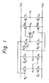
- Figs. 1 to 3 of the accompanying drawings illustrate a conventional buffer circuit which amplifies an input clock signal ⁇ 0 ("clock ⁇ 0 ") with impedance conversion and supplies an output clock signal ⁇ 1 ("clock ⁇ 1 ").
- the circuit comprises MOS transistors Ql to Q8 and Q10 to Q12, Q9 being an MOS capacitor.
- the input stage of the buffer circuit is a delay circuit comprising the transistors Ql to Q4. During a standby period, the delay circuit holds the voltage of a node N2, which connects the source of the transistor Q3 to the drain of the transistor Q4, at a high level by using the input clock ⁇ 0 and an inverted input clock signal ⁇ 0 ("clock ⁇ 0 ").
- the clock ⁇ 0 is at a high level during an active period and is at a low level during the standby period.
- the clock ⁇ 0 because of the inverted polarity, is at a low level during the active period and is at a high level during the standby period.
- These clock signals turn off the transistor Q1; turn on the transistors Q2 and Q3; hold a node N1 at a low level, which node connects the source of the transistor Ql to the drain of the transistor Q2 and the gate of the transistor Q4; turn off the transistor Q4; and charge the node N2 to a voltage (Vcc-Vth) via the transistor Q3 during the standby period.
- Vcc is the voltage at the high potential side of the power supply.
- Vth is a threshold voltage of the transistor Q3.
- the gate of the transistor Q5 is connected to the power supply Vcc. Hence, when the node N2 is charged to the voltage (Vcc-Vth), a node N3 is charged to the same voltage.
- the node N3 connects the transistor Q5 to the gate of-the transistor Q6 to form the gate terminal of the transistor Q6 in a bootstrap circuit comprising the transistors Q6 and Q7.
- the charged voltage of the node N3 drives an output stage comprising the transistors Q8 and Q10 to Q12 at a high speed during the next active period.
- the transistor Q7 Since the clock ⁇ 0 is at a high level during the standby period, the transistor Q7 turns on; a node N4,which interconnects the source of the transistor Q6, the drain of the transistor Q7, the MOS capacitor Q9 and the gate of transistor Qll,turns to a low level; the transistors Q8 and Qll turn off; and the transistors Q10 and Q12 turn on.
- the output clock ⁇ 1 is at the low level, which is equal to the low potential side Vss of the power supply (usually ground potential).
- the input clocks and W o are inverted.
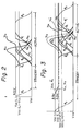
- waveforms of the operation are shown during the active period, and this example shows the case where Vcc is constant and equal to 4.5 volts. Since, in this example, the voltage of the node N2 is equal to the voltage of the node N3, and the voltage of these nodes is (4.5 volts-Vth), when the clock ⁇ 0 is changed from Vcc to Vss and the clock ⁇ 0 is raised from Vss to Vcc, the voltage of the nodeN3 rises above (Vcc+Vth) and the voltage of the node N4 is charged to the voltage of ⁇ 0 , which is equal to Vcc, by the bootstrap effect, which is caused by the effects of the capacitance between the gate and the drain of the transistor Q6 and between the gate and the source of the transistor Q6.
- the voltage of the clock 4 0 is low, the voltage of the clock ⁇ 0 is high and the voltage Vcc is 5.5 volts, causing both the nodes N2 and N3 to be charged up to the voltage of (5.5 volts-Vth).
- the voltage Vcc decreases to 4.5 volts during the standby period, the voltages of the nodes N2 and N3 (5.5 volts-Vth) do not change, because there is no discharge path.
- the reason there is no discharge path is that the transistor Q4 holds off, and the transistor Q3 goes to the off state because the gate voltage of Q3 changes to 4.5 volts from 5.5 volts due to the power supply fluctuation.
- waveforms indicated by lines N2', N3', N5' and ⁇ 1 ' show the variation with time of the voltages at the nodes N2, N3 and N5 and the voltage of the clock ⁇ 1 without a power supply fluctuation, as compared with broken lines N2, N3, N5 and ⁇ 1 , which show the variation of the corresponding voltages when a fluctuation occurs in the power supply.
- An object of the present invention is to provide a semiconductor buffer circuit in which the delay in the output clock caused by fluctuation of the voltage of the power supply is decreased, thereby providing a shorter access time.
- a semiconductor buffer circuit to be energised by a power supply and comprising an input stage for receiving an input clock signal and an inverted input clock signal; a bootstrap circuit including a first transistor to receive the output of the input stage and to maintain the gate voltage of said first transistor at a high level during a standby period; and an output circuit including a second transistor which is switched on and off by the output of the bootstrap circuit to generate an output clock signal, characterised by a current leak circuit for maintaining, during the standby period, the voltage of a point in the semiconductor circuit which is charged during the standby period to a level corresponding to the voltage of the power supply.
- a semiconductor buffer circuit comprising an input stage delay circuit to receive an input clock signal and an inverted input clock signal; a bootstrap circuit including a node to receive the output of the input stage delay circuit, the bootstrap circuit being operative to raise the voltage of the node by the bootstrap operation; and an output circuit to receive the output of the bootstrap circuit and to generate an output clock signal; characterised by a current leak circuit connected between the node and one pole of a power supply, whereby the voltage of a point in the semiconductor circuit which is charged during a standby period is always maintained during the standby period at a value corresponding to the voltage of the power supply.
- a semiconductor buffer circuit comprising an input stage delay circuit for receiving an input clock signal and an inverted input clock signal; a bootstrap circuit including a node to receive the output of the input stage delay circuit, a first stage transistor and a second stage transistor, and being operative to raise the voltage of the node by the bootstrap operation; and an output circuit for receiving the output of the bootstrap circuit and for generating an output clock signal; characterised by a current leak circuit connected between the node which connects the first stage transistor to the second stage transistor and one of the poles of a power supply, whereby the voltage of a point in the semiconductor circuit which is charged during a standby period is always maintained during the standby period at a value corresponding to the voltage of the power supply.
- a semiconductor buffer circuit comprising an input stage delay circuit to receive an input clock signal and an inverted input clock signal; a bootstrap circuit including a node for receiving the output of the input stage delay circuit, the bootstrap circuit being operative to raise the voltage of the node by the bootstrap operation, the bootstrap circuit including a first transistor and a second transistor in a first stage and a transistor in a second stage; and an output circuit for receiving the output of the bootstrap circuit and for generating an output clock signal; characterised by two current leak circuits, one of which connects a first node to one pole of a power supply, which first node connects the first transistor and the second transistor in the first stage with the transistor in the second stage, and the other of which connects the second node to one of the poles of the power supply, the second node connecting the second transistor in the first stage with the output of the input stage delay circuit; whereby the voltages of points in the semiconductor circuit which are charged during a standby period are always maintained during the standby
- a semiconductor buffer circuit has a power source fluctuation compensating circuit (current leak circuit) X enclosed by a broken line.
- the circuit X comprises a series connection of an enhancement-type MOS transistor Q13 for a leaking current turned on during a standby period and a depletion- type MOS transistor Q14 for limiting the current.
- the circuit X is connected between the node N2 and the low voltage side Vss of the power supply.
- the node N2 is the connecting node between the transistor Q3, which turns on during the standby period and is used for charging, and the transistor Q4, which turns on during an active period and is used for discharging.
- the "on" and "off” states of the transistor Q13 are controlled by the clock ⁇ 0 , but alternatively another signal which corresponds to the clock ⁇ 0 in the IC can be used instead of the clock ⁇ 0 for this purpose.
- a resistor rl a resistor rl
- the transistor Q14 can be omitted, if the resistance of the transistor Q13 can be made high by adjusting the width/length of the channel thereof (Fig.10b).
- a resistor r2 can be used (Fig.10c).
- the function required of the circuit X is to allow a small amount of current to leak during the standby period to cause the voltage of the nodes N2 and N3 to fall to the voltage (Vcc-Vth) at that time.
- the nodes N2 and N3 are charged at the beginning of the standby period to a voltage of (5.5 volts-Vth) by the voltage Vcc which is equal to 5.5 volts; then, when the voltage Vcc falls to 4.5 volts, the charge on the node N2 is discharged through the circuit X until the voltage of the node N2 falls to (4.5 volts-Vth), as shown in Fig.5.
- the voltage of the node N2 falls, more specifically, to a voltage of (4.5 volts-Vth-AV), where the voltage drop AV is caused by the resistance of the transistor Q3 when that transistor turns on.
- the voltage drop ⁇ V is negligible.
- the transistor Q5 turns on, the charge on the node N3 flows to the node N2, and the voltage of the node N3 changes to be equal to the voltage of (4.5 volts-Vth- ⁇ V), which is equal to the voltage of the node N2. Therefore, the effect of the decrease in Vcc from 5.5 volts to 4.5 volts, namely the delay in the rising of the clock ⁇ 1 , does not appear during the active period, if the voltage of Vcc changes from 5.5 volts to 4.5 volts during the standby period. Since the current which flows through the circuit X is very small, the charging of the node N2 takes place unhindered.
- the transistor 13 is not necessary. Since the nodes N2 and N3 are charged through the transistor Q3, if the circuit X consists of only a leakage resistance the voltages of the nodes N2 and N3 can be held to the voltage of (Vcc-Vth) at that time.
- the clock ⁇ 5 does not synchronise with the clock ⁇ 0 ; in some cases the clock ⁇ 0 falls and after a while the clock . 0 rises.
- the circuit X consists of only ⁇ a leakage resistance, the voltages of the nodes N2 and N3 would fall excessively between the falling time of the clock ⁇ 0 and the rising time of the clock ⁇ 0 , and, accordingly, the transistor Q13 is necessary.
- the waveforms for the latter case are shown in broken lines in Fig.5.
- the voltage Vth of the transistor Q3 is equal to the voltage Vth of the transistor Q5. If the voltage Vth of the transistor Q5 is higher than that of the transistor Q3 because of non-uniformity of the transistor characteristics due to the manufacturing process, the transistor Q5 remains off, but nevertheless the voltage of the node N2 falls to the voltage (Vcc-Vth- ⁇ V). Then, although the voltage of the node N2 falls as described above, the voltage of the node N3 cannot fall. If the voltage of the node N3 is high, as mentioned above, the voltage of the node N3 rises higher during the active period, and then the rising of the output clock ⁇ 1 is delayed.
- a semiconductor buffer circuit according to a second embodiment of the present invention is shown.
- the power supply fluctuation compensating circuit current leak circuit
- the voltage of the node N3 can be the voltage (Vcc-Vth).
- Fig.7 the waveforms occurring in the operation of the circuit in Fig.6 are shown.
- the voltage of the node N2 discharges through the transistor Q5 and the circuit X and falls to the voltage (Vcc-Vth), the value of which is similar to the node N3.
- the waveforms in the circuit of Fig.6, produced without the circuit X are shown by broken lines in Fig.7, which can be compared with the solid lines which indicate the waveforms of the circuit of Fig.6 produced with the circuit X.
- the electrostatic capacity of the node N3 increases and the bootstrap effect is interrupted at the rising time of the clock ⁇ 0 and then the increase in the voltages of the nodes N3 and N4 is interrupted.
- FIG.8 another example of a conventional clock amplifier circuit uses two transistors Q51 and Q52, instead of the transistor Q5 of Fig.l.
- the transistor Q3 turns on; the voltage of the node N2 is (Vcc-Vth); the transistor Q51 turns on; and the voltage of the node N3 is (Vcc-Vth).
- the transistor Q52 turns off and the node N2 is separated from the node N3.
- the transistor Q52 turns on and the circuit in Fig.8 operates similarly to the circuit of Fig.l. Also, in the case in which the voltage Vcc changes before the active period, the voltages of the nodes N2 and N3 remain at an excessively high level. In this circuitry, if a power source fluctuation compensating circuit is connected to either the node N2 or the node N3, since the transistor Q52 is off during the standby period, when the voltage of the power supply changes, the voltage of the node to which the power supply fluctuation compensating circuit is not connected remains at a high voltage.
- a semiconductor buffer circuit is proposed, according to a third embodiment of the present invention, as shown in Fig.9.
- two power source fluctuation compensating circuits X and X' are connected between the node N2 and Vss and between the node N3 and Vss, respectively.
- the voltage of the power supply rises from 4.5 volts to 5.5 volts.
- the voltage of the clock ⁇ 0 rises from 4.5 volts to 5.5 volts, for the following reasons.
- the clock ⁇ 0 is generated by a similar circuit to that shown in Fig.1, and when the voltage of Vcc is 4.5 volts and the voltage of the clock ⁇ 1 is at a high level (4.5 volts), the voltage of the node N4 is greater than (Vcc+Vth) i.e. (4.5 volts + Vth). Also, the voltage of the node N5 is the voltage Vcc.
- the voltage of the node N5 rises from 4.5 volts to 5.5 volts through the transistor Q8. Since the voltage of the node N5 increases the voltage of the node N4 through the transistor Q9, although the voltage of Vcc rises to 5.5 volts, the voltage of the node N4 rises to the voltage of (Vcc+Vth), i.e. (5.5 volts + Vth), and the voltage of the clock ⁇ 1 rises to 5.5 volts.
- the voltage of the nodes N2 and N3 is equal to the voltage of the nodes when the voltage Vcc is fixed at 5.5 volts. Hence, there is no delay in the operating time.
Abstract
Description
- This invention relates to a semiconductor buffer circuit which compensates for power supply fluctuations. The circuit may, for example, be used for amplification of a clock signal in a dynamic memory.
- Figs. 1 to 3 of the accompanying drawings illustrate a conventional buffer circuit which amplifies an input clock signal φ0 ("clock φ0") with impedance conversion and supplies an output clock signal φ1 ("clock φ1"). The circuit comprises MOS transistors Ql to Q8 and Q10 to Q12, Q9 being an MOS capacitor. The input stage of the buffer circuit is a delay circuit comprising the transistors Ql to Q4. During a standby period, the delay circuit holds the voltage of a node N2, which connects the source of the transistor Q3 to the drain of the transistor Q4, at a high level by using the input clock φ0 and an inverted input clock signal
φ 0 ("clockφ 0"). The clock φ0 is at a high level during an active period and is at a low level during the standby period. The clockφ 0, because of the inverted polarity, is at a low level during the active period and is at a high level during the standby period. These clock signals turn off the transistor Q1; turn on the transistors Q2 and Q3; hold a node N1 at a low level, which node connects the source of the transistor Ql to the drain of the transistor Q2 and the gate of the transistor Q4; turn off the transistor Q4; and charge the node N2 to a voltage (Vcc-Vth) via the transistor Q3 during the standby period. Vcc is the voltage at the high potential side of the power supply. It is usually 5 volts, which is the standard value, allowing for an error of - 10%. Vth is a threshold voltage of the transistor Q3. The gate of the transistor Q5 is connected to the power supply Vcc. Hence, when the node N2 is charged to the voltage (Vcc-Vth), a node N3 is charged to the same voltage. The node N3 connects the transistor Q5 to the gate of-the transistor Q6 to form the gate terminal of the transistor Q6 in a bootstrap circuit comprising the transistors Q6 and Q7. By charging the node N3 to a high level during the standby period, the charged voltage of the node N3 drives an output stage comprising the transistors Q8 and Q10 to Q12 at a high speed during the next active period. Since the clockφ 0 is at a high level during the standby period, the transistor Q7 turns on; a node N4,which interconnects the source of the transistor Q6, the drain of the transistor Q7, the MOS capacitor Q9 and the gate of transistor Qll,turns to a low level; the transistors Q8 and Qll turn off; and the transistors Q10 and Q12 turn on. The output clock φ1 is at the low level, which is equal to the low potential side Vss of the power supply (usually ground potential). - On entering the active period, the input clocks and Wo are inverted. In Fig.2, waveforms of the operation are shown during the active period, and this example shows the case where Vcc is constant and equal to 4.5 volts. Since, in this example, the voltage of the node N2 is equal to the voltage of the node N3, and the voltage of these nodes is (4.5 volts-Vth), when the clock
φ 0 is changed from Vcc to Vss and the clock φ0 is raised from Vss to Vcc, the voltage of the nodeN3 rises above (Vcc+Vth) and the voltage of the node N4 is charged to the voltage of φ0, which is equal to Vcc, by the bootstrap effect, which is caused by the effects of the capacitance between the gate and the drain of the transistor Q6 and between the gate and the source of the transistor Q6. - This results in the transistors Q8 and Qll being turned on. At the same time, since the transistor Ql turns on, the transistor Q2 turns off; the node N1 is charged up and the transistor Q4 turns on; then the voltage of the node N2 begins the decrease. Accordingly, the electric charge on the node N3 is reduced through the transistor Q5 and the voltage of the nodes N3 and N2 decreases to the voltage Vss. When the voltage of the node N2 falls to a value of (Vss+Vth) the transistors Q10 and Q12 turn off and the voltage of the node N5 rises to Vcc. At this time, since the voltage of the node N4 is raised above the voltage (Vcc+Vth) through the capacitor Q9, the output clock φ1 rises to the maximum voltage level Vcc.
- The above operation has been described on the assumption that no fluctuation in the power supply level occurs. However, as shown in Fig.3, if a variation in the power supply voltage does occur during the standby period, the output clock φ1 is delayed, and this delay poses a problem. In Fig.3 an example is shown in which the value of Vcc decreases from 5.5 volts (Vcc(U)) to 4.5 volts (Vcc(L)) during the standby period. The above-mentioned fluctuation occurs, or the fluctuation of other devices connected to the power source occur, because the electrical structure of the constant voltage power supply is simplified in order to reduce the production cost. During the standby period the voltage of the clock 40 is low, the voltage of the clock
φ 0 is high and the voltage Vcc is 5.5 volts, causing both the nodes N2 and N3 to be charged up to the voltage of (5.5 volts-Vth). However, if the voltage Vcc decreases to 4.5 volts during the standby period, the voltages of the nodes N2 and N3 (5.5 volts-Vth) do not change, because there is no discharge path. The reason there is no discharge path is that the transistor Q4 holds off, and the transistor Q3 goes to the off state because the gate voltage of Q3 changes to 4.5 volts from 5.5 volts due to the power supply fluctuation. When the voltage of the nodes N2 and N3 is held, the rising of the clock φ1 is delayed. In order to raise the clock φ1, it is necessary that the transistors Q10 and Q12 are turned off. However, it takes time for the voltage of the node N2 to fall to the low level at which the transistors Q10 and Q12 are turned off, because the voltage of the node N2 is 1 volt higher than the voltage of (4.5 volts-Vth) in Fig.2. During the delay time when the voltage is falling at the node N2, a delay in the rising of the clock t, occurs. In Fig.3, waveforms indicated by lines N2', N3', N5' and φ1' show the variation with time of the voltages at the nodes N2, N3 and N5 and the voltage of the clock φ1 without a power supply fluctuation, as compared with broken lines N2, N3, N5 and φ1, which show the variation of the corresponding voltages when a fluctuation occurs in the power supply. - An object of the present invention is to provide a semiconductor buffer circuit in which the delay in the output clock caused by fluctuation of the voltage of the power supply is decreased, thereby providing a shorter access time.
- According to one aspect of the present invention, there is provided a semiconductor buffer circuit to be energised by a power supply and comprising an input stage for receiving an input clock signal and an inverted input clock signal; a bootstrap circuit including a first transistor to receive the output of the input stage and to maintain the gate voltage of said first transistor at a high level during a standby period; and an output circuit including a second transistor which is switched on and off by the output of the bootstrap circuit to generate an output clock signal, characterised by a current leak circuit for maintaining, during the standby period, the voltage of a point in the semiconductor circuit which is charged during the standby period to a level corresponding to the voltage of the power supply.
- According to another aspect of the present invention, there is provided a semiconductor buffer circuit comprising an input stage delay circuit to receive an input clock signal and an inverted input clock signal; a bootstrap circuit including a node to receive the output of the input stage delay circuit, the bootstrap circuit being operative to raise the voltage of the node by the bootstrap operation; and an output circuit to receive the output of the bootstrap circuit and to generate an output clock signal; characterised by a current leak circuit connected between the node and one pole of a power supply, whereby the voltage of a point in the semiconductor circuit which is charged during a standby period is always maintained during the standby period at a value corresponding to the voltage of the power supply.
- According to a further aspect of the present invention, there is provided a semiconductor buffer circuit comprising an input stage delay circuit for receiving an input clock signal and an inverted input clock signal; a bootstrap circuit including a node to receive the output of the input stage delay circuit, a first stage transistor and a second stage transistor, and being operative to raise the voltage of the node by the bootstrap operation; and an output circuit for receiving the output of the bootstrap circuit and for generating an output clock signal; characterised by a current leak circuit connected between the node which connects the first stage transistor to the second stage transistor and one of the poles of a power supply, whereby the voltage of a point in the semiconductor circuit which is charged during a standby period is always maintained during the standby period at a value corresponding to the voltage of the power supply.
- According to another aspect of the present invention, there is provided a semiconductor buffer circuit comprising an input stage delay circuit to receive an input clock signal and an inverted input clock signal; a bootstrap circuit including a node for receiving the output of the input stage delay circuit, the bootstrap circuit being operative to raise the voltage of the node by the bootstrap operation, the bootstrap circuit including a first transistor and a second transistor in a first stage and a transistor in a second stage; and an output circuit for receiving the output of the bootstrap circuit and for generating an output clock signal; characterised by two current leak circuits, one of which connects a first node to one pole of a power supply, which first node connects the first transistor and the second transistor in the first stage with the transistor in the second stage, and the other of which connects the second node to one of the poles of the power supply, the second node connecting the second transistor in the first stage with the output of the input stage delay circuit; whereby the voltages of points in the semiconductor circuit which are charged during a standby period are always maintained during the standby period at a value corresponding to the voltage of the power supply.
- Embodiments of the invention will now be described, by way of example, with reference to the accompanying drawings, in which:
- Figs. 1, 2 and 3 are a circuit diagram and waveform diagrams, respectively, of an example of a conventional clock amplifier circuit as described above,
- Fig.4 is a circuit diagram of a semiconductor buffer circuit according to a first embodiment of the present invention,
- Fig.5 is a waveform diagram of the circuit of Fig.4,
- Fig.6 is a circuit diagram of a semiconductor buffer circuit according to a second embodiment of the present invention,
- Fig.7 is a waveform diagram of the circuit of Fig.6,
- Fig.8 is a circuit diagram of another example of a conventional clock amplifier circuit,
- Fig.9 is a circuit diagram of a semiconductor buffer circuit according to a third embodiment of the present invention,
- Figs. 10a, b and c are circuit diagrams showing various modified current leak circuits used for embodiments of the present invention.
- Referring to Fig.4, a semiconductor buffer circuit according to a first embodiment of the present invention has a power source fluctuation compensating circuit (current leak circuit) X enclosed by a broken line. Such circuit is not provided in the conventional circuit of Fig.l. The circuit X comprises a series connection of an enhancement-type MOS transistor Q13 for a leaking current turned on during a standby period and a depletion- type MOS transistor Q14 for limiting the current. The circuit X is connected between the node N2 and the low voltage side Vss of the power supply. The node N2 is the connecting node between the transistor Q3, which turns on during the standby period and is used for charging, and the transistor Q4, which turns on during an active period and is used for discharging. In this example the "on" and "off" states of the transistor Q13 are controlled by the clock
φ 0, but alternatively another signal which corresponds to the clockφ 0 in the IC can be used instead of the clockφ 0 for this purpose. - Furthermore, alternative current control elements can be substituted in place of the transistor Q14, such as a resistor rl (Fig.10a). Furthermore, the transistor Q14 can be omitted, if the resistance of the transistor Q13 can be made high by adjusting the width/length of the channel thereof (Fig.10b). Also, instead of the transistors Q13 and Q14, a resistor r2 can be used (Fig.10c). Thus, the function required of the circuit X is to allow a small amount of current to leak during the standby period to cause the voltage of the nodes N2 and N3 to fall to the voltage (Vcc-Vth) at that time.
- When the above-mentioned power source fluctuation compensating circuit X is connected, the nodes N2 and N3 are charged at the beginning of the standby period to a voltage of (5.5 volts-Vth) by the voltage Vcc which is equal to 5.5 volts; then, when the voltage Vcc falls to 4.5 volts, the charge on the node N2 is discharged through the circuit X until the voltage of the node N2 falls to (4.5 volts-Vth), as shown in Fig.5. In the above description the voltage of the node N2 falls, more specifically, to a voltage of (4.5 volts-Vth-AV), where the voltage drop AV is caused by the resistance of the transistor Q3 when that transistor turns on. However, the voltage drop ΔV is negligible. When the voltage of the node N2 falls to (4.5 volts-Vth-AV), the transistor Q5 turns on, the charge on the node N3 flows to the node N2, and the voltage of the node N3 changes to be equal to the voltage of (4.5 volts-Vth- ΔV), which is equal to the voltage of the node N2. Therefore, the effect of the decrease in Vcc from 5.5 volts to 4.5 volts, namely the delay in the rising of the clock φ1, does not appear during the active period, if the voltage of Vcc changes from 5.5 volts to 4.5 volts during the standby period. Since the current which flows through the circuit X is very small, the charging of the node N2 takes place unhindered.
- In a circuit in which the clock
φ 0 synchronizes with the clock φ0 and the falling of the clock $0 and the rising of the clock φ1 occur simultaneously, the transistor 13 is not necessary. Since the nodes N2 and N3 are charged through the transistor Q3, if the circuit X consists of only a leakage resistance the voltages of the nodes N2 and N3 can be held to the voltage of (Vcc-Vth) at that time. - However, usually the clock
φ 5 does not synchronise with the clock φ0; in some cases the clockφ 0 falls and after a while the clock .0 rises. In this case, if the circuit X consists of only·a leakage resistance, the voltages of the nodes N2 and N3 would fall excessively between the falling time of the clockφ 0 and the rising time of the clock φ0, and, accordingly, the transistor Q13 is necessary. In order to compare this with the case in which no current leak circuit X is provided, the waveforms for the latter case are shown in broken lines in Fig.5. - In the above-mentioned embodiment, it is assumed that the voltage Vth of the transistor Q3 is equal to the voltage Vth of the transistor Q5. If the voltage Vth of the transistor Q5 is higher than that of the transistor Q3 because of non-uniformity of the transistor characteristics due to the manufacturing process, the transistor Q5 remains off, but nevertheless the voltage of the node N2 falls to the voltage (Vcc-Vth- ΔV). Then, although the voltage of the node N2 falls as described above, the voltage of the node N3 cannot fall. If the voltage of the node N3 is high, as mentioned above, the voltage of the node N3 rises higher during the active period, and then the rising of the output clock φ1 is delayed.
- In Fig.6, a semiconductor buffer circuit according to a second embodiment of the present invention is shown. In order to solve the above-mentioned problems, in the circuit in Fig.6 the power supply fluctuation compensating circuit (current leak circuit) is connected to the node N3. By using the power source fluctuation compensating circuit, the voltage of the node N3 can be the voltage (Vcc-Vth).
- In Fig.7, the waveforms occurring in the operation of the circuit in Fig.6 are shown. The voltage of the node N2 discharges through the transistor Q5 and the circuit X and falls to the voltage (Vcc-Vth), the value of which is similar to the node N3. The waveforms in the circuit of Fig.6, produced without the circuit X, are shown by broken lines in Fig.7, which can be compared with the solid lines which indicate the waveforms of the circuit of Fig.6 produced with the circuit X. If the circuit X is connected at the node N3, according to the second embodiment, the electrostatic capacity of the node N3 increases and the bootstrap effect is interrupted at the rising time of the clock φ0 and then the increase in the voltages of the nodes N3 and N4 is interrupted.
- In Fig.8, another example of a conventional clock amplifier circuit uses two transistors Q51 and Q52, instead of the transistor Q5 of Fig.l. In this circuit, during the standby period, since the clock
φ 0 is at a high level, the transistor Q3 turns on; the voltage of the node N2 is (Vcc-Vth); the transistor Q51 turns on; and the voltage of the node N3 is (Vcc-Vth). Then, since the voltage of the clock φ0 is at a low level, the transistor Q52 turns off and the node N2 is separated from the node N3. During the active period, since the voltage of the clock $0 is at a high level, the transistor Q52 turns on and the circuit in Fig.8 operates similarly to the circuit of Fig.l. Also, in the case in which the voltage Vcc changes before the active period, the voltages of the nodes N2 and N3 remain at an excessively high level. In this circuitry, if a power source fluctuation compensating circuit is connected to either the node N2 or the node N3, since the transistor Q52 is off during the standby period, when the voltage of the power supply changes, the voltage of the node to which the power supply fluctuation compensating circuit is not connected remains at a high voltage. - In order to solve this problem, a semiconductor buffer circuit is proposed, according to a third embodiment of the present invention, as shown in Fig.9. In this circuit, two power source fluctuation compensating circuits X and X'are connected between the node N2 and Vss and between the node N3 and Vss, respectively.
- Below, the cases are explained in which the voltage of the power supply is fixed at 5.5 volts, and in which the voltage of the power supply rises up from 4.5 volts to 5.5 volts, respectively.
- In the case in which the voltage of the power supply is-5.5 volts, generally at the high voltage of the power supply the mutual conductance gm increases; then the operating speed increases and there is no bad influence. An explanation is given referring to Fig.l. When the voltage of the power supply Vcc is high, the voltages of the nodes N2 and N3 are high and the high level of the clock φ0 rises further. Then the voltage of the node N1 rises further and the gm of the transistor Q4 is higher than the gm of the transistor Q4 at the low value of Vcc. Since the gm of the transistor Q4 is high, the discharging speed at the nodes N2 and N3 is high.
- Now the case will be described in which the voltage of the power supply rises from 4.5 volts to 5.5 volts. When Vcc rises from 4.5 volts to 5.5 volts, the voltage of the clock
φ 0 rises from 4.5 volts to 5.5 volts, for the following reasons. The clockφ 0 is generated by a similar circuit to that shown in Fig.1, and when the voltage of Vcc is 4.5 volts and the voltage of the clock φ1 is at a high level (4.5 volts), the voltage of the node N4 is greater than (Vcc+Vth) i.e. (4.5 volts + Vth). Also, the voltage of the node N5 is the voltage Vcc. Hence, when the voltage Vcc rises from 4.5 volts to 5.5 volts, the voltage of the node N5 rises from 4.5 volts to 5.5 volts through the transistor Q8. Since the voltage of the node N5 increases the voltage of the node N4 through the transistor Q9, although the voltage of Vcc rises to 5.5 volts, the voltage of the node N4 rises to the voltage of (Vcc+Vth), i.e. (5.5 volts + Vth), and the voltage of the clock φ1 rises to 5.5 volts. - After the voltage Vcc has risen from 4.5 volts to 5.5 volts, the voltage of the nodes N2 and N3 is equal to the voltage of the nodes when the voltage Vcc is fixed at 5.5 volts. Hence, there is no delay in the operating time.
Claims (8)
Applications Claiming Priority (2)
| Application Number | Priority Date | Filing Date | Title |
|---|---|---|---|
| JP162889/80 | 1980-11-19 | ||
| JP55162889A JPS5788594A (en) | 1980-11-19 | 1980-11-19 | Semiconductor circuit |
Publications (2)
| Publication Number | Publication Date |
|---|---|
| EP0052504A1 true EP0052504A1 (en) | 1982-05-26 |
| EP0052504B1 EP0052504B1 (en) | 1985-06-12 |
Family
ID=15763173
Family Applications (1)
| Application Number | Title | Priority Date | Filing Date |
|---|---|---|---|
| EP81305415A Expired EP0052504B1 (en) | 1980-11-19 | 1981-11-16 | Semiconductor buffer circuit |
Country Status (5)
| Country | Link |
|---|---|
| US (1) | US4447745A (en) |
| EP (1) | EP0052504B1 (en) |
| JP (1) | JPS5788594A (en) |
| DE (1) | DE3170954D1 (en) |
| IE (1) | IE52354B1 (en) |
Cited By (3)
| Publication number | Priority date | Publication date | Assignee | Title |
|---|---|---|---|---|
| EP0109004A2 (en) * | 1982-11-15 | 1984-05-23 | International Business Machines Corporation | Low power clock generator |
| FR2538191A1 (en) * | 1982-12-20 | 1984-06-22 | Western Electric Co | AMPLIFIER WITH PAIR OF TRANSISTORS WITH GRATING COUPLING FIELD EFFECT |
| EP0233734A2 (en) * | 1986-02-08 | 1987-08-26 | Fujitsu Limited | Clock signal generating circuit |
Families Citing this family (11)
| Publication number | Priority date | Publication date | Assignee | Title |
|---|---|---|---|---|
| JPS595488A (en) * | 1982-07-01 | 1984-01-12 | Fujitsu Ltd | Semiconductor device |
| JPS599735A (en) * | 1982-07-07 | 1984-01-19 | Mitsubishi Electric Corp | Clock generating circuit |
| US4484087A (en) * | 1983-03-23 | 1984-11-20 | General Electric Company | CMOS latch cell including five transistors, and static flip-flops employing the cell |
| JPS60140924A (en) * | 1983-12-27 | 1985-07-25 | Nec Corp | Semiconductor circuit |
| US4599520A (en) * | 1984-01-31 | 1986-07-08 | International Business Machines Corporation | Boosted phase driver |
| US4728820A (en) * | 1986-08-28 | 1988-03-01 | Harris Corporation | Logic state transition detection circuit for CMOS devices |
| US6798269B2 (en) * | 2000-07-25 | 2004-09-28 | Stmicroelectronics S.R.L. | Bootstrap circuit in DC/DC static converters |
| JP4846223B2 (en) * | 2004-10-12 | 2011-12-28 | 株式会社アドバンテスト | Test apparatus and test method |
| JP5665299B2 (en) * | 2008-10-31 | 2015-02-04 | 三菱電機株式会社 | Shift register circuit |
| JP5188382B2 (en) | 2008-12-25 | 2013-04-24 | 三菱電機株式会社 | Shift register circuit |
| JP5484109B2 (en) | 2009-02-09 | 2014-05-07 | 三菱電機株式会社 | Electro-optic device |
Citations (5)
| Publication number | Priority date | Publication date | Assignee | Title |
|---|---|---|---|---|
| US3774055A (en) * | 1972-01-24 | 1973-11-20 | Nat Semiconductor Corp | Clocked bootstrap inverter circuit |
| DE2417994A1 (en) * | 1974-01-16 | 1975-07-24 | Hitachi Ltd | COMPENSATION DEVICE FOR ELECTRONIC CIRCUITS |
| US4015219A (en) * | 1974-01-16 | 1977-03-29 | Hitachi, Ltd. | Electronic circuit using field effect transistor with compensation means |
| DE2625007B2 (en) * | 1975-06-04 | 1978-11-30 | Hitachi, Ltd., Tokio | Address buffer circuit for semiconductor memories |
| EP0032017A1 (en) * | 1979-12-19 | 1981-07-15 | Fujitsu Limited | Bootstrap circuit |
Family Cites Families (3)
| Publication number | Priority date | Publication date | Assignee | Title |
|---|---|---|---|---|
| US4061933A (en) * | 1975-12-29 | 1977-12-06 | Mostek Corporation | Clock generator and delay stage |
| US4239990A (en) * | 1978-09-07 | 1980-12-16 | Texas Instruments Incorporated | Clock voltage generator for semiconductor memory with reduced power dissipation |
| US4354123A (en) * | 1979-08-13 | 1982-10-12 | Mostek Corporation | High voltage clock generator |
-
1980
- 1980-11-19 JP JP55162889A patent/JPS5788594A/en active Granted
-
1981
- 1981-11-16 DE DE8181305415T patent/DE3170954D1/en not_active Expired
- 1981-11-16 EP EP81305415A patent/EP0052504B1/en not_active Expired
- 1981-11-18 IE IE2705/81A patent/IE52354B1/en not_active IP Right Cessation
- 1981-11-18 US US06/322,719 patent/US4447745A/en not_active Expired - Fee Related
Patent Citations (6)
| Publication number | Priority date | Publication date | Assignee | Title |
|---|---|---|---|---|
| US3774055A (en) * | 1972-01-24 | 1973-11-20 | Nat Semiconductor Corp | Clocked bootstrap inverter circuit |
| DE2417994A1 (en) * | 1974-01-16 | 1975-07-24 | Hitachi Ltd | COMPENSATION DEVICE FOR ELECTRONIC CIRCUITS |
| FR2258051A1 (en) * | 1974-01-16 | 1975-08-08 | Hitachi Ltd | |
| US4015219A (en) * | 1974-01-16 | 1977-03-29 | Hitachi, Ltd. | Electronic circuit using field effect transistor with compensation means |
| DE2625007B2 (en) * | 1975-06-04 | 1978-11-30 | Hitachi, Ltd., Tokio | Address buffer circuit for semiconductor memories |
| EP0032017A1 (en) * | 1979-12-19 | 1981-07-15 | Fujitsu Limited | Bootstrap circuit |
Cited By (5)
| Publication number | Priority date | Publication date | Assignee | Title |
|---|---|---|---|---|
| EP0109004A2 (en) * | 1982-11-15 | 1984-05-23 | International Business Machines Corporation | Low power clock generator |
| EP0109004A3 (en) * | 1982-11-15 | 1985-05-15 | International Business Machines Corporation | Low power clock generator |
| FR2538191A1 (en) * | 1982-12-20 | 1984-06-22 | Western Electric Co | AMPLIFIER WITH PAIR OF TRANSISTORS WITH GRATING COUPLING FIELD EFFECT |
| EP0233734A2 (en) * | 1986-02-08 | 1987-08-26 | Fujitsu Limited | Clock signal generating circuit |
| EP0233734A3 (en) * | 1986-02-08 | 1989-03-29 | Fujitsu Limited | Clock signal generating circuit |
Also Published As
| Publication number | Publication date |
|---|---|
| IE812705L (en) | 1982-05-19 |
| JPS5788594A (en) | 1982-06-02 |
| IE52354B1 (en) | 1987-09-30 |
| US4447745A (en) | 1984-05-08 |
| EP0052504B1 (en) | 1985-06-12 |
| DE3170954D1 (en) | 1985-07-18 |
| JPS6137709B2 (en) | 1986-08-25 |
Similar Documents
| Publication | Publication Date | Title |
|---|---|---|
| KR100467918B1 (en) | Semiconductor integrated circuit with valid voltage conversion circuit at low operating voltage | |
| US4943745A (en) | Delay circuit for semiconductor integrated circuit devices | |
| EP0052504A1 (en) | Semiconductor buffer circuit | |
| KR980006526A (en) | Intermediate voltage generator circuit and nonvolatile semiconductor memory having the same | |
| US4443714A (en) | Semiconductor buffer circuit having compensation for power source fluctuation | |
| US5901055A (en) | Internal boosted voltage generator of semiconductor memory device | |
| US4649289A (en) | Circuit for maintaining the potential of a node of a MOS dynamic circuit | |
| US6215329B1 (en) | Output stage for a memory device and for low voltage applications | |
| US4239991A (en) | Clock voltage generator for semiconductor memory | |
| KR970006605B1 (en) | Voltage generating circuit causing no threshold voltage loss by fet in output voltage | |
| US5627739A (en) | Regulated charge pump with low noise on the well of the substrate | |
| US4352996A (en) | IGFET Clock generator circuit employing MOS boatstrap capacitive drive | |
| US4716303A (en) | MOS IC pull-up circuit | |
| KR100215535B1 (en) | Semiconductor memory device | |
| US4490627A (en) | Schmitt trigger circuit | |
| US5175448A (en) | Booster circuit | |
| US5579276A (en) | Internal voltage boosting circuit in a semiconductor memory device | |
| EP0170781A2 (en) | MOS dynamic memory device | |
| US6430093B1 (en) | CMOS boosting circuit utilizing ferroelectric capacitors | |
| US4529889A (en) | Sense amplifier latch voltage waveform generator circuit | |
| JP3053178B2 (en) | Semiconductor integrated circuit | |
| JPH0798982A (en) | Substrate bias circuit | |
| KR100432985B1 (en) | Circuit for generating increased output voltage | |
| US6353560B1 (en) | Semiconductor memory device | |
| KR950000533B1 (en) | Data output buffer |
Legal Events
| Date | Code | Title | Description |
|---|---|---|---|
| PUAI | Public reference made under article 153(3) epc to a published international application that has entered the european phase |
Free format text: ORIGINAL CODE: 0009012 |
|
| AK | Designated contracting states |
Designated state(s): DE FR GB NL |
|
| 17P | Request for examination filed |
Effective date: 19820921 |
|
| GRAA | (expected) grant |
Free format text: ORIGINAL CODE: 0009210 |
|
| AK | Designated contracting states |
Designated state(s): DE FR GB NL |
|
| REF | Corresponds to: |
Ref document number: 3170954 Country of ref document: DE Date of ref document: 19850718 |
|
| ET | Fr: translation filed | ||
| PLBE | No opposition filed within time limit |
Free format text: ORIGINAL CODE: 0009261 |
|
| STAA | Information on the status of an ep patent application or granted ep patent |
Free format text: STATUS: NO OPPOSITION FILED WITHIN TIME LIMIT |
|
| 26N | No opposition filed | ||
| PGFP | Annual fee paid to national office [announced via postgrant information from national office to epo] |
Ref country code: GB Payment date: 19921106 Year of fee payment: 12 |
|
| PGFP | Annual fee paid to national office [announced via postgrant information from national office to epo] |
Ref country code: FR Payment date: 19921127 Year of fee payment: 12 |
|
| PGFP | Annual fee paid to national office [announced via postgrant information from national office to epo] |
Ref country code: NL Payment date: 19921130 Year of fee payment: 12 |
|
| PGFP | Annual fee paid to national office [announced via postgrant information from national office to epo] |
Ref country code: DE Payment date: 19930129 Year of fee payment: 12 |
|
| PG25 | Lapsed in a contracting state [announced via postgrant information from national office to epo] |
Ref country code: GB Effective date: 19931116 |
|
| PG25 | Lapsed in a contracting state [announced via postgrant information from national office to epo] |
Ref country code: NL Effective date: 19940601 |
|
| GBPC | Gb: european patent ceased through non-payment of renewal fee |
Effective date: 19931116 |
|
| NLV4 | Nl: lapsed or anulled due to non-payment of the annual fee | ||
| PG25 | Lapsed in a contracting state [announced via postgrant information from national office to epo] |
Ref country code: FR Effective date: 19940729 |
|
| PG25 | Lapsed in a contracting state [announced via postgrant information from national office to epo] |
Ref country code: DE Effective date: 19940802 |
|
| REG | Reference to a national code |
Ref country code: FR Ref legal event code: ST |