EP0051525B1 - Logic array with simplified electric programming - Google Patents
Logic array with simplified electric programming Download PDFInfo
- Publication number
- EP0051525B1 EP0051525B1 EP81401683A EP81401683A EP0051525B1 EP 0051525 B1 EP0051525 B1 EP 0051525B1 EP 81401683 A EP81401683 A EP 81401683A EP 81401683 A EP81401683 A EP 81401683A EP 0051525 B1 EP0051525 B1 EP 0051525B1
- Authority
- EP
- European Patent Office
- Prior art keywords
- inputs
- variable
- logic
- signals
- matrix
- Prior art date
- Legal status (The legal status is an assumption and is not a legal conclusion. Google has not performed a legal analysis and makes no representation as to the accuracy of the status listed.)
- Expired
Links
Images


Classifications
-
- H—ELECTRICITY
- H03—ELECTRONIC CIRCUITRY
- H03K—PULSE TECHNIQUE
- H03K19/00—Logic circuits, i.e. having at least two inputs acting on one output; Inverting circuits
- H03K19/02—Logic circuits, i.e. having at least two inputs acting on one output; Inverting circuits using specified components
- H03K19/173—Logic circuits, i.e. having at least two inputs acting on one output; Inverting circuits using specified components using elementary logic circuits as components
- H03K19/177—Logic circuits, i.e. having at least two inputs acting on one output; Inverting circuits using specified components using elementary logic circuits as components arranged in matrix form
- H03K19/17704—Logic circuits, i.e. having at least two inputs acting on one output; Inverting circuits using specified components using elementary logic circuits as components arranged in matrix form the logic functions being realised by the interconnection of rows and columns
- H03K19/17708—Logic circuits, i.e. having at least two inputs acting on one output; Inverting circuits using specified components using elementary logic circuits as components arranged in matrix form the logic functions being realised by the interconnection of rows and columns using an AND matrix followed by an OR matrix, i.e. programmable logic arrays
- H03K19/17712—Logic circuits, i.e. having at least two inputs acting on one output; Inverting circuits using specified components using elementary logic circuits as components arranged in matrix form the logic functions being realised by the interconnection of rows and columns using an AND matrix followed by an OR matrix, i.e. programmable logic arrays one of the matrices at least being reprogrammable
Definitions
- the present invention relates to programmable logic networks, that is to say integrated circuits having n logic signal inputs and m outputs, and capable of providing on each of the outputs a particular logical combination, programmed, of the binary signals applied to the starters.
- This logical combination is expressed as a logical sum of several logical products of the input signals.
- These outputs are network outputs.
- the goal of network programming is to have each output define a particular chosen combination of input variables, expressed as a sum of the products of some of these variables.
- Network programming therefore consists in defining the AND matrix to obtain products of certain input variables, and in defining the OR matrix to obtain sums of some of the products produced.
- the AND gates of the AND matrix can receive all the inputs of variables a and their complements; after programming they only receive the variables selected to make a particular product; the others must be disconnected so that there is no influence, on a particular product, of a variable a which does not appear in this product.
- the OR gates of the OR matrix can receive before programming all the outputs of the AND gates, that is to say that they can add all the p intermediate products calculated by the AND matrix; after programming, an OR gate corresponding to an output of the network must receive on its inputs only the intermediate products appearing in the logical combination to be produced on this output; the outputs of the other AND gates, corresponding to products which should not appear in the sum, must be disconnected.
- the present invention is concerned with networks which are electrically programmable by the user and not those which are programmed in manufacturing by masking techniques.
- the electrical programming of the network requires having individual electrical access to all the inputs of the AND gates and the OR gates, in total at 2n x p AND gate inputs added to p x m OR gate inputs.
- These figures correspond to 1536 programming points to be carried out. Each of these points must be individually accessible to apply an adequate programming signal (for example an electric voltage capable of destroying a fuse in series with a diode in a particularly simple embodiment).
- the programming seen from the user side consists in selecting the door inputs which must receive a neutralization signal, in applying this signal to them, and in leaving the other inputs active.
- a programmable logic network using this principle is the IM5200 circuit from the company INTERSIL which is electrically programmable; in this circuit, two of the variable inputs A are used to define the transition to programming mode, four network outputs are used, in programming mode, to designate matrix sectors AND and OR to be programmed, and nine variable inputs are used, in programming mode, designate the door inputs to be disconnected.
- the invention provides a programmable logic network characterized by the fact that it includes a decoder capable of individually designating each of the output columns of the product matrix as well as an input line of the sum matrix corresponding to the same product. intermediary than the designated column, a logic interface circuit connecting said matrices, capable of generating, from the output signal of the decoder and write command signals from a control circuit, programming signals of the designated column and the corresponding line of the sum matrix, the network further comprising an input interface circuit for generating, from write signals applied to the variable inputs and write command signals from the control circuit, programming signals for lines of the matrix produced, these signals being such that the intermediate product obtained at the output of the column designated in mode of reading, after programming by the row and column programming signals, that is to say a product of the variables corresponding to the inputs of variables to which a particular writing signal has been applied.
- the decoder designates a particular intermediate product, and the variable inputs Ai are used in programming, to establish this intermediate product, with the same meaning as in normal use.
- an output interface circuit capable of generating, from write signals applied to the network outputs used as inputs and from write control signals of the command, programming signals from the columns of the sum matrix, these signals being such that the intermediate product designated by the decoder appears in read mode on those of the outputs to which a particular write signal has been applied during programming.
- This programming mode is therefore extremely simple for the user who, in the digital example already used, is spared the need to know a (binary) correspondence between eleven address inputs and 1536 door inputs to be programmed.
- the first complicating factor comes from the fact that we want to use only n input pins of variables Ai while the logical combinations to be made by the network can include either these variables a or their complements at i . In reading, there is no difficulty because information is introduced in two states: presence of a or its complement, and binary signals 0 or 1 applied to n inputs a are sufficient to completely specify the input information .
- connection pins which would make the invention lose a large part of its interest (we would have the programming simplification at the price of n additional pins, which is hardly acceptable).
- This two-step writing procedure for each intermediate product can be carried out thanks to the locking function of the input and output interface circuits.
- the input interface circuit switches the first part of the write signal applied to an input of variable Ai to an input line of the matrix produced corresponding to this variable Ai, and it switches the second part to the input line corresponding to the complement Ai of this variable.
- the test operations of the programmed matrices are done with the same simplification as the programming operations; the test is also done simultaneously for the two matrices which remain independent in test as in programming.
- the logic circuit for interfacing the interface between matrices is capable of generating, from the output signal of the decoder designating a particular intermediate product and from test control signals coming from the control circuit, a signal of result-- test state of the designated intermediate product, this signal being transmitted to a test reading output.
- the input interface circuit it is able to generate, from logic test signals applied to the variable inputs and test command signals from the control circuit, matrix line test signals product, applied to the input lines of this matrix in such a way that there is a direct correspondence between the application of a particular test signal on each variable input and the application of a line test signal on a row of the product matrix corresponding to this variable.
- the invention makes it possible to carry out the programming test while keeping the variable inputs the same meaning as they have in reading (and in writing).
- the test can be done door by door entry to check the neutralization of each connection, or more generally door by door.
- the test signals applied to the variable inputs Ai can be exactly the same as the particular write signals: signals with two successive pieces of information introduced in two stages, two successive 1s on Ai producing a line test signal on a matrix line corresponding to the variable a ;, two successive 0's produce a line test signal on a line corresponding to at i , and a 1 and a 0 simultaneously producing a test signal on lines a and i .
- the input interface circuit therefore operates in exactly the same way in writing and in testing.
- the output interface circuit which makes it possible to carry out the test of the sum matrix, does not function in the same way in writing and in test.
- the outputs Si are still used initially in a test step to address the decoder and designate an intermediate product.
- the link interface circuit between matrices generates, from the decoder signal and test command signals coming from the control circuit, a line test signal applied to the input line of the sum matrix designated by the decoder. While the output interface circuit keeps in memory the addressing of the decoder, the outputs Si of the network then operate, in a second stage of a test step, as outputs of the gates of the sum matrix, and supply the result of the test with a direct correspondence between the logic level obtained on each output and the actual presence of the designated intermediate product in the programmed logic combination corresponding to this output.
- the input interface circuit transmits the logic signals appearing on the inputs Ai on the one hand directly to a line of the product matrix and of elsewhere after inversion to a neighboring line.
- the output interface circuit directly transmits the outputs of the columns of the sum matrix to the respective outputs Si.
- the link interface interface between matrices connects the output of each column of matrix produced to a respective input line of the sum matrix.
- field effect transistors of the MNOS metal - nitride - oxide - semiconductor type are used to program the connection of each variable input to a respective AND gate input, or the connection of each AND gate output to a respective OR gate input.
- An MNOS transistor has the remarkable possibility of performing an erasable electrical programming, of being able to be permanently made non-conductive by applying a high voltage to its control gate which traps electrons at the interface between the layer nitride and the oxide layer. The trapped electrons remain trapped in this interface when the high voltage disappears and they keep the MNOS transistor blocked; the subsequent application to the control gate of a voltage which would normally make the transistor conductive now has no effect on it.
- This trapping can also be erased electrically by applying a high voltage in the opposite direction.
- Transistors which have not been subjected to the high trapping voltage normally behave as transistors, that is to say that they can be blocked or made conductive depending on the voltage applied to their gate.
- NOR gates can only comprise MNOS transistors in parallel, one per gate input, the control gates serving as inputs, the sources being grounded and all the drains (connected between them and constituting the output of the NOR gate) being connected to a positive voltage through a common charge.
- each NOR gate comprises several independent inputs which are the gates of the transistors, a connection connection of the drains between them, a connection connection of the sources between them and a connection of supply voltage.
- the transistors can be adequately polarized so that they perform the NOR function, - in programming mode (erase first then write), apply the appropriate voltages on the connections allowing the “trapping” or not of the transistors.
- the application of the appropriate programming polarizations or voltages is carried out by the input, output, and link interface circuits, under the control of the control circuit.
- the programming or test signals generated by these circuits consist of determined voltage configurations at the electrodes of the MNOS transistors (zero or normal or high voltage or high impedence link).
- FIG. 1 the block diagram of a programmable logic network: from n inputs of variables Ao to An-1 we can introduce logic signals a o - a n-1 and their complements 8 0 to a n-1 of 2 n input lines of an AND gate matrix (p AND gates with 2 n inputs each) which provides at its output intermediate logic products Mo to Mp-1 input variables a (direct or complemented). Each of the intermediate products is determined by those of the input variables or their complements which are effectively coupled to the AND gate inputs.
- the intermediate products Mi constitute both output columns of the AND matrix and input lines of an OR gate matrix (m OR gates with p inputs each) which supplies, on its output columns So to Sm- 1, logical combinations of the input variables ao to a n-1 in the form of sums of intermediate products of the variables.
- Each of the sums is determined by the effective coupling between certain columns of intermediate products and the inputs of the OR gate corresponding to this sum.
- Network programming to obtain the desired logical combination on each of the outputs consists in selecting the connections to be made between the variable inputs and the AND gates, as well as between the outputs of the AND matrix and the OR gate inputs.
- Fig. 2 shows a logic network equivalent to that of FIG. 1 but where the product and sum matrices (AND and OR matrices) are produced with NOR gates (NON-OR).
- An AND gate can indeed be replaced by a NOR gate, each input of which is preceded by an inverter; an OR gate by a NOR gate followed by an inverter.
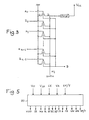
- Fig. 3 shows an example of NOR gate with n inputs a o , a 1 ... a n-1 , produced using field effect transistors.
- N-channel MNOS metal-nitride-oxide-semiconductor transistors. They could be other types of transistors without departing from the scope of the invention, but these are particularly suitable for electrical network programming.
- the sources of the transistors are all assembled and connected to ground, the drains are all joined together and connected to a common load connected to a normal supply voltage Vcc.
- the substrates are all connected to a common voltage, in principle of 0 volts.
- Each transistor control gate serves as an input to the NOR gate and the output is taken from the combined drains.
- Logic signals a o , at o , a i , at 1 ..., at n-1 are used to block or unblock the transistors.
- the conduction of one or more transistors by a level 1 logic signal sets the output to zero. Blocking all transistors simultaneously sets the output to 1. It is therefore a NOR door.
- the programming of the door consists in suppressing or putting in permanent blocking the transistors corresponding to the variables which must not influence the output; for example, producing the product a i to j at output consists in removing or blocking all the transistors connected to the other inputs that at i and a ⁇ ; similarly, realize the sum a + at j would consist in keeping as active transistors only those connected to inputs a and at j .
- MNOS transistors as door elements is particularly advantageous since it offers a convenient possibility of electrical programming to neutralize the influence of a NOR door input on its output.
- This neutralization is done by putting the MNOS transistor in a permanent blocking state by trapping electrons at the interface of its two oxide layers; trapped electrons maintain the threshold voltage of the transistor at a high value (around 7 V) and create an unlocking voltage threshold that cannot be crossed by a normal logic signal (0 to 5 V) applied to the gate.
- the non “trapped” transistors are conductive or blocked according to their gate voltage because their threshold voltage is low: 1 to 2 volts.
- Trapping is done by applying a high voltage to the grid (about 25 volts). It is non-destructive and reversible: we can evacuate trapped electrons towards the substrate by applying a high voltage on it. It is then an electrical erasure of the programming, all the transistors returning to their normal state.
- the role of the network interface circuits will be to apply the appropriate voltages to the grid lines, the source and drain columns, and the combined substrates, according to operating mode signals (read, erase, write, test) and according to the logic signals applied to the various inputs of the network, including the outputs used as inputs.
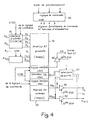
- a decoder (40) capable of individually designating each of the output columns of the AND matrix as well as the input line of the OR matrix corresponding to the same intermediate product as the column of designated outlet.
- This designation is intended for the interface logic circuit which applies the voltages suitable to the column and to the designated line.
- the decoder is constituted for example simply by a series of p AND or NOR gates which receive binary addresses used for the designation of the chosen column and which have programmed inputs (definitively) so that each possible address opens one and only one door among the p decoder doors.
- the decoder is used mainly in write mode but also in test mode.
- the binary addresses it receives are brought by external connection pins with the help of which the user chooses the column of transistors to be programmed in the AND matrix. These pins are, for the sake of reducing the number of external pins, preferably chosen from pins used for other purposes in read mode. However, they are not taken from the input pins of variables Ao to An-1 which are used for another use during programming.
- the addressing inputs of the decoder in write mode are taken from the outputs So to Sm-1 of the network, which then operate as inputs.
- There is actually a need r for the decoder addressing inputs such that 2 r-1 ⁇ p ⁇ 2 r ; for example, if the network includes 64 intermediate products, 6 addressing inputs chosen from the outputs So to Sm-1 can be used.
- These r inputs, split into 2 X r with their logical complements, are applied to the p doors constituting the decoder.
- the outputs So to Sm-1 can operate as outputs of the OR gates of the OR matrix, and also as inputs for the decoder, there is interposed between the OR gate outputs and the Si terminals of buffer amplifiers (50) with three states , with a third state command isolating the outputs Si from the outputs SOi of the OR matrix.
- the setting in the third state is carried out in write mode and is deleted in read mode. In test mode, we will see that it is used partially.
- the output terminals Si (So to Sm-1) are therefore connected to the inputs of the decoder, but by means of an output interface circuit (60) having in particular a role of locking and routing as we want , in writing mode, use the outputs Si not only as addressing inputs for the decoder (firstly writing), but also secondly as writing inputs proper by which we can designate those MNOS transistors of the OR matrix which must be blocked (the decoder only indicating which input line of the OR matrix we are interested in during a programming step).
- the output interface circuit (60) is there to keep in memory the addressing of the decoder while the writing data which are directed to the outputs SOi of the OR gates (drains together of the transistors) are introduced on the terminals. MNOS).
- the write vectors are introduced and stored in memory in input interface circuits (70) which, in write mode and moreover also in test mode, decode the two information bits introduced on each variable entry Ai to designate that of the two grid lines of MNOS corresponding to Ai which is to be programmed or tested.
- the programming work is simple and the programming of the AND and OR matrices is simultaneous. It is carried out step by step, each step corresponding to an intermediate product to be produced, therefore to a column of transistor drains in parallel for the AND matrix and to a line of gates in parallel for the OR matrix.
- a logic control circuit (80) which receives information or operating voltage levels from the outside to define the working mode and the instants of triggering of write cycles as well as the synchronization of data entries in programming and test mode.
- This logic circuit better symbolized in fig. 5, establishes functional control signals transmitted to the various interface logic circuits (30, 60, 70), to the third state controls of the buffer amplifiers etc.
- This control logic circuit (80) in particular has functions for converting voltage levels when necessary, including for providing a compatibility interface between circuits of different technologies.
- a TM output downstream of a three-state amplifier (90). It is a test output allowing to examine, in test mode, the output of each of the columns of transistors of the AND matrix, to determine if the application of a given logical vector on the inputs Ai causes on each door exit AND (chosen by the decoder) the expected logical result.
- test operations which are carried out in a similar way to those of writing, and for the two matrices at the same time, one can say that the operator introduces test signals on the inputs Ai, that is to say on a entry at a time, either by vectors. These vectors are introduced in two stages and they designate the input lines of the AND matrix that we are examining. During this time, a given intermediate product address (therefore a column of the AND matrix and an input line of the OR matrix) is introduced on the outputs Si (first step of the test step).
- control circuit (80) establishes various control signals applied to the interface circuits to make the transistors of the two arrays apply the conditions of erasing, writing, testing, or reading.
- control circuit (80) The realization of the various functions of the control circuit (80) is a pure affair of combinatorial logic, and the use of buffer amplifiers (buffers) when it comes to making conversions of logic voltage levels. It is not necessary to give the details of the logic gate diagrams establishing each control function.
- fig. 6 shows the logic circuit (30) for interfacing links between matrices with the decoder (40), this at the level of a single column j of MNOS transistors of the AND matrix; only one MNOS transistor 101 of the ET matrix has been shown, the one whose gate must receive a high trapping voltage if the variable a must appear in the intermediate product corresponding to the column j considered.
- This transistor 101 receives on its gate a voltage Vai which can be zero or 5 volts or 25 volts. (See fig. 7 for the production of this voltage by the input interface circuit 70.)
- the source can be grounded or airborne depending on the state of the F8 function.
- the drain corresponds to the output SCj of column ET (in fact NOR), and it can be connected to a load supplied by Vpp (in reading), or put in the air (erasure) or put at a protection voltage Vp ( write when the column is not selected), or finally set to zero (write when column j is selected).
- the substrate of the MNOS transistor can be set to 0 volts or to Vpp depending on the state of the function F7.
- the various doors of the interface logic of FIG. 6 have been shown in detail to show how they establish the various voltage or impedance levels at the terminals of the MNOS transistor of the line i and of the column j from the output state of the gate j of the decoder and of the various outputs of the control logic circuit.
- the interface logic circuit (30) also imposes a determined output voltage on the conductor LOj which is the input line j of the OR matrix (input on a gate of transistor MNOS).
- the signal on LOj is the same as SCj; it is besides the only case where one has a direct transmission between the matrix AND and the matrix OR.
- the line Vp is used both to bring a write or erase protection voltage (see fig. 10), and also to collect the state of SCj (isolated from LOj at this time) in test mode.
- Fig. 7 shows how the appropriate voltage is produced on the input lines a; at i leading to the gates of the MNOS transistors of the AND matrix; the diagram is an exemplary embodiment using the signal SL (reading mode) to connect via transfer gates 701 and 702 the input Ai to line a and, with an inverter, to the line at i . Outside the reading mode, the EF / T signal is applied to two gates 703 and 704 capable of transmitting the voltage VIDD on the lines a i and at i .
- a zero voltage is applied to the grid lines a and at i ; in test and write, the applied voltage depends on the logic signal applied to the input Ai.
- the locking buffer amplifier 705 does not change state and the voltage a remains unchanged.
- the signal VA2 then begins, at the same time as a second bit of test or write information is loaded at the input Ai, which is transmitted in complemented form, by another locking buffer amplifier 706 which also plays the role of reverser and through gate 704, at the line at i .
- a 1 on Ai brings 0 volts on at i while a zero brings 5 volts.
- a 1 on Ai brings 0 volts on to; while a zero brings 25 volts.
- Fig. 9 shows an exemplary embodiment of an output interface circuit (60) making it possible to receive a decoder address or write data from the OR matrix from the outputs Si of the network; the diagram of the three-state amplifier (50) making it possible to use the outputs Si as well in outputs connected to the outputs SOi of the matrix OR as in addressing inputs or in data inputs, is also shown in the drawing of fig. 9.
- AMi and AMi the decoder address lines
- addressing signal stored in memory on AMi and AMi designating a given intermediate product which is applied (see fig. 6) on the input lines of the OR matrix (LOj), and a write voltage VIDD or zero on the columns SOi.
- the output SOi is also connected, for reading or testing, to Si via the three-state amplifier 50, controlled by the signal F8, which prevents direct return, in writing or at first. of the test of the signal of Si to the columns SOi.
- MNOS transistors Other programmable and electrically erasable transistors can be used (floating gate transistors for example).
Description
La présente invention concerne les réseaux logiques programmables, c'est-à-dire des circuits intégrés possédant n entrées de signaux logiques et m sorties, et capables de fournir sur chacune des sorties une combinaison logique particulière, programmée, des signaux binaires appliqués sur les entrées. Cette combinaison logique s'exprime sous forme d'une somme logique de plusieurs produits logiques des signaux d'entrée.The present invention relates to programmable logic networks, that is to say integrated circuits having n logic signal inputs and m outputs, and capable of providing on each of the outputs a particular logical combination, programmed, of the binary signals applied to the starters. This logical combination is expressed as a logical sum of several logical products of the input signals.
Dans le cas général, un réseau logique programmable possède deux matrices de portes, à savoir:
- - d'une part une matrice produit qui consiste en une série de p portes logiques de 2n entrées chacune; ces entrées sont couplées à certaines des n entrées Ai, complémentées ou non du réseau, et les sorties des portes fournissent des signaux qui sont des produits des variables d'entrée a, reçues; on désigne ces produits par le terme «produits intermédiaires»; ils sont au nombre de p s'il y a p portes; cette matrice produit s'appelle généralement matrice ET et les portes sont des portes ET ou réalisent l'équivalent logique d'une fonction ET;
- - d'autre part une matrice somme ou matrice OU qui consiste en une série de m portes (autant que de sorties du réseau, c'est-à-dire que de combinaisons logiques différentes à réaliser); ces portes sont des portes OU, ou en réalisent l'équivalent logique; elles ont chacune p entrées couplées respectivement à certaines des sorties de p portes ET de la matrice ET; les sorties des m portes OU fournissent des sommes logiques des signaux appliqués à leurs entrées, c'est-à-dire des sommes des produits des variables d'entrée.
- - on the one hand, a product matrix which consists of a series of p logic gates of 2n inputs each; these inputs are coupled to some of the n inputs Ai, whether or not complemented by the network, and the outputs of the gates provide signals which are products of the input variables a, received; these products are designated by the term "intermediate products"; there are p if there are gates; this produced matrix is generally called AND matrix and the gates are AND gates or realize the logical equivalent of an AND function;
- - on the other hand, a sum matrix or OR matrix which consists of a series of m gates (as many as network outputs, that is to say that of different logical combinations to be produced); these doors are OR doors, or realize their logical equivalent; they each have p inputs coupled respectively to some of the outputs of p AND gates of the AND matrix; the outputs of the m OR gates provide logical sums of the signals applied to their inputs, that is to say sums of the products of the input variables.
Ces sorties sont les sorties du réseau.These outputs are network outputs.
Le but de la programmation du réseau est de faire en sorte que chaque sortie définisse une combinaison particulière choisie des variables d'entrée, exprimée sous forme d'une somme de produits de certaines de ces variables.The goal of network programming is to have each output define a particular chosen combination of input variables, expressed as a sum of the products of some of these variables.
On peut faire ici une parenthèse pour indiquer que le raisonnement serait identique si on inversait les positions des matrices OU et ET pour réaliser en sortie des combinaisons logiques exprimées sous forme de produits de sommes. L'algèbre de Boole montre qu'une telle inversion est possible sans difficultés, et on se contentera de décrire l'invention pour des sommes de produits.One can make here a parenthesis to indicate that the reasoning would be identical if one reversed the positions of the matrices OR and AND to carry out as output logical combinations expressed in the form of products of sums. Boole's algebra shows that such an inversion is possible without difficulty, and we will content ourselves with describing the invention for sums of products.
La programmation du réseau consiste donc à définir la matrice ET pour obtenir des produits de certaines variables d'entrée, et à définir la matrice OU pour obtenir des sommes de certains des produits réalisés.Network programming therefore consists in defining the AND matrix to obtain products of certain input variables, and in defining the OR matrix to obtain sums of some of the products produced.
Par exemple, pour obtenir les combinaisons
- S, =
a 1 a2 a3 + a1a 2 - et S2 = a1 a3 + a1 à2
dans un réseau à trois entrées et deux sorties, il faut:
- 1. réaliser une porte ET recevant
a 1, a2 et a3, une autre recevant a1 et â2 et une troisième recevant a1 et a3. - 2. réaliser une porte OU recevant la sortie des première et deuxième portes ET,et une autre recevant la sortie des deuxième et troisième portes ET.
- S, =
at 1 to 2 to 3 + to 1at 2 - and S 2 = a 1 to 3 + a 1 to 2
in a network with three inputs and two outputs, you must:
- 1. make a door AND receiving
at 1 , a 2 and a 3 , another receiving a 1 and a 2 and a third receiving a 1 and a 3 . - 2. make an OR gate receiving the output of the first and second AND gates, and another receiving the output of the second and third AND gates.
Avant programmation, les portes ET de la matrice ET peuvent recevoir toutes les entrées de variables a et leurs compléments; après programmation elles ne reçoivent que les variables sélectionnées pour faire un produit particulier; les autres doivent être déconnectées pour qu'il n'y ait pas d'influence, sur un produit particulier, d'une variable a n'apparaissant pas dans ce produit.Before programming, the AND gates of the AND matrix can receive all the inputs of variables a and their complements; after programming they only receive the variables selected to make a particular product; the others must be disconnected so that there is no influence, on a particular product, of a variable a which does not appear in this product.
De même, les portes OU de la matrice OU peuvent recevoir avant programmation toutes les sorties des portes ET, c'est-à-dire qu'elles peuvent additionner tous les p produits intermédiaires calculés par la matrice ET; après programmation, une porte OU correspoondant à une sortie du réseau ne doit recevoir sur ses entrées que les produits intermédiaires apparaissant dans la combinaison logique à réaliser sur cette sortie; les sorties des autres portes ET, correspondant à des produits ne devant pas apparaître dans la somme, doivent être déconnectées.Similarly, the OR gates of the OR matrix can receive before programming all the outputs of the AND gates, that is to say that they can add all the p intermediate products calculated by the AND matrix; after programming, an OR gate corresponding to an output of the network must receive on its inputs only the intermediate products appearing in the logical combination to be produced on this output; the outputs of the other AND gates, corresponding to products which should not appear in the sum, must be disconnected.
La présente invention s'intéresse aux réseaux qui sont programmables électriquement par l'utilisateur et non à ceux qui sont programmés en fabrication par des techniques de masquage.The present invention is concerned with networks which are electrically programmable by the user and not those which are programmed in manufacturing by masking techniques.
Le problème à résoudre est le suivant: la programmation électrique du réseau nécessite d'avoir un accès électrique individuel à toutes les entrées des portes ET et des portes OU, au total à 2n x p entrées de portes ET ajoutées à p x m entrées de portes OU. Par exemple, on peut avoir 8 entrées se décomposant en 16 avec leurs compléments, 8 sorties et 64 produits intermédiaires (les nombres n, m et p sont indépendants et déterminent la capacité globale du réseau). Ces chiffres correspondent à 1536 points de programmation à effectuer. Chacun de ces points doit être accessible individuellement pour appliquer un signal de programmation adéquat (par exemple une tension électrique capable de détruire un fusible en série avec une diode dans une réalisation particulièrement simple).The problem to be solved is as follows: the electrical programming of the network requires having individual electrical access to all the inputs of the AND gates and the OR gates, in total at 2n x p AND gate inputs added to p x m OR gate inputs. For example, we can have 8 inputs broken down into 16 with their complements, 8 outputs and 64 intermediate products (the numbers n, m and p are independent and determine the overall capacity of the network). These figures correspond to 1536 programming points to be carried out. Each of these points must be individually accessible to apply an adequate programming signal (for example an electric voltage capable of destroying a fuse in series with a diode in a particularly simple embodiment).
La programmation vue du côté de l'utilisateur consiste à sélectionner les entrées de portes qui doivent recevoir un signal de neutralisation, à leur appliquer ce signal, et à laisser les autres entrées actives.The programming seen from the user side consists in selecting the door inputs which must receive a neutralization signal, in applying this signal to them, and in leaving the other inputs active.
S'il y a un nombre de points de programmation aussi élevé que 1536, on peut prévoir que 11 entrées binaires (211 = 2048) serviront à désigner chacune des portes à travers un décodeur, pour diriger exclusivement vers la porte désignée le signal de programmation. Il est impératif, pour des raisons de minimisation du nombre de broches de connexions extérieures du circuit intégré, que ces entrées soient prises parmi les broches existant obligatoirement sur le circuit intégré, par exemple les broches correspondant aux entrées Ao et An-1 et aux sorties So à Sm-1, ces broches n'ayant alors pas la même fonction en mode normal de calcul logique et en mode exceptionnel de programmation (une entrée spéciale pouvant définir le mode).If there is a number of programming points as high as 1536, it can be foreseen that 11 binary inputs (2 11 = 2048) will be used to designate each of the doors through a decoder, to direct exclusively to the designated door the signal of programming. It is imperative, for reasons of minimization of the number of pins of external connections of the integrated circuit, that these inputs are taken from among the pins obligatorily existing on the integrated circuit, for example the pins corresponding to the inputs Ao and An-1 and to the outputs So to Sm-1, these pins then not having the same function in normal logic calculation mode and in exceptional programming mode (a special input can define the mode).
Pour l'opérateur, le problème est le suivant, il faut:
- - qu'il établisse les formules des diverses combinaisons logiques à réaliser (les diverses sommes de produits des variables d'entrée ai); et qu'il affecte à chacune une sortie du réseau, c'est-à-dire une porte OU déterminée;
- - qu'il établisse une liste de tous les produits intermédiaires apparaissant dans les diverses combinaisons logiques; et qu'il affecte une porte ET à chacun d'eux;
- - qu'il détermine, pour un produit particulier donc pour une porte ET respective, quelles sont les entrées de cette porte ET à neutraliser, compte tenu de la correspondance entre les entrées a; du réseau et les entrées des portes ET; cette correspondance est directe puisque chaque entrée A du réseau est connectée à une entrée respective de toutes les portes ET;
- - qu'il prévoie, avant de passer en programmation, l'adressage de chacune des entrées à neutraliser, compte tenu de la correspondance prévue par le fabricant, entre les entrées d'adressage et les entrées des portes ET à neutraliser; mais cette fois, même si ce sont les entrées A;, c'est-à-dire les entrées de variables, qui servent aussi d'entrées d'adressage en mode programmation, la correspondance n'est plus du tout directe; elle se fait à travers un codage binaire à cause du grand nombre (2n x p) de points de programmation à adresser dans la matrice ET;
- - après avoir fait ces opérations et programmé toute la matrice ET, il faut encore que l'opérateur détermine, pour une combinaison logique particulière à réaliser, donc pour une porte OU respective, quelles sont les entrées de cette porte OU qu'il faut neutraliser, compte tenu de la correspondance entre la liste des produits intermédiaires qu'il a établie et les positions d'entrées de porte OU connectées aux sorties de produits intermédiaires;
- - enfin, il faut que l'opérateur prévoie, avant de passer en programmation de la matrice OU, l'adressage de chacune des entrées de porte OU à neutraliser, compte-tenu de la correspondance prévue par le fabricant, en mode de programmation, entre les entrées d'adressage et les entrées de porte OU à déconnecter; cette correspondance est évidemment encore tout à fait indirecte et l'utilisateur doit en connaître le codage binaire; si ce sont encore les entrées de variable a qui servent d'entrées d'adressage de la matrice OU en mode de programmation, cela fait une correspondance de plus à connaître pour le programmeur entre les numéros de broches extérieures du réseau et la structure interne de celui-ci.
- - that it establishes the formulas of the various logical combinations to be carried out (the various sums of products of the input variables a i ); and that it assigns to each an output of the network, that is to say a determined OR gate;
- - establish a list of all the intermediate products appearing in the various logical combinations; and that it assigns an AND gate to each of them;
- - that it determines, for a particular product therefore for a respective AND gate, which are the inputs of this AND gate to be neutralized, taking into account the correspondence between the inputs a; of the network and the inputs of the AND gates; this correspondence is direct since each input A of the network is connected to a respective input of all the AND gates;
- - that it provides, before entering programming, the addressing of each of the inputs to be neutralized, taking into account the correspondence provided by the manufacturer, between the addressing inputs and the inputs of the doors AND to be neutralized; but this time, even if it is the inputs A ;, that is to say the variable inputs, which also serve as addressing inputs in programming mode, the correspondence is no longer direct at all; it is done through binary coding because of the large number (2n xp) of programming points to be addressed in the AND matrix;
- - after having made these operations and programmed the whole AND matrix, the operator must also determine, for a particular logical combination to be carried out, therefore for a respective OR gate, which are the inputs of this OR gate which must be neutralized , taking into account the correspondence between the list of intermediate products which it established and the positions of door inputs OR connected to the outputs of intermediate products;
- - finally, the operator must provide, before going into programming the OR matrix, the addressing of each of the OR gate inputs to be neutralized, taking into account the correspondence provided by the manufacturer, in programming mode, between the addressing inputs and the OR gate inputs to be disconnected; this correspondence is obviously still quite indirect and the user must know the binary coding thereof; if it is still the variable inputs a which serve as addressing inputs for the matrix OR in programming mode, this makes one more correspondence for the programmer to know between the external pin numbers of the network and the internal structure of this one.
Un exemple de réseau logique programmable utilisant ce principe est le circuit IM5200 de la société INTERSIL qui est programmable électriquement; dans ce circuit, deux des entrées de variable A servent à définir le passage en mode de programmation, quatre sorties du réseau servent, en mode de programmation, à désigner des secteurs de matrice ET et OU à programmer, et neuf entrées de variables servent, en mode de programmation, à désigner les entrées de portes à déconnecter.An example of a programmable logic network using this principle is the IM5200 circuit from the company INTERSIL which is electrically programmable; in this circuit, two of the variable inputs A are used to define the transition to programming mode, four network outputs are used, in programming mode, to designate matrix sectors AND and OR to be programmed, and nine variable inputs are used, in programming mode, designate the door inputs to be disconnected.
Le travail très important du programmeur peut se justifier car il s'agit d'un réseau non reprogrammable. Toutefois, il serait souhaitable, même dans ce cas, de réduire ce travail; il est de toutes façons nécessaire d'y parvenir si le réseau est effaçable et reprogrammable électriquement, faute de quoi l'intérêt de la reprogrammation disparaîtrait devant la difficulté de celle-ci.The very important work of the programmer can be justified because it is a non-reprogrammable network. However, it would be desirable, even in this case, to reduce this work; it is in any case necessary to achieve this if the network is erasable and reprogrammable electrically, failing which the interest of reprogramming would disappear in the face of its difficulty.
Tel est le but que cherche à atteindre la présente invention en proposant un réseau logique programmable - qui présente une grande facilité d'utilisation lors de la programmation, - qui permet en particulier de programmer simultanément la matrice ET et la matrice OU contrairement à ce qui se faisait jusqu'à maintenant, - qui permet l'utilisation directe des entrées de variables A avec une signification commune en mode de lecture et en mode de programmation de la matrice ET, - qui de préférence ne nécessite pas de broches de connexion supplémentaires pour l'adressage des entrées des portes de la matrice ET et de la matrice OU en mode de programmation, - qui permet un test après programmation pour la vérification individuelle soit de la programmation de chaque porte ET ou OU, soit même de cellé de chaque entrée de porte ET ou OU, avec une grande facilité d'adressage des portes ou entrées à tester, - qui permet aussi, dans le cas du test de la programmation de chaque porte, d'effectuer simultanément le test de la matrice ET et de la matrice OU.This is the aim that the present invention seeks to achieve by proposing a programmable logic network - which has great ease of use during programming, - which makes it possible in particular to simultaneously program the AND matrix and the OR matrix, unlike what was done until now, - which allows the direct use of the inputs of variables A with a common meaning in reading mode and in programming mode of the matrix AND, - which preferably does not require additional connection pins for addressing the inputs of the AND matrix and OR matrix gates in programming mode, - which allows a test after programming for individual verification either of the programming of each AND or OR gate, or even of each input cell AND or OR door, with great ease of addressing the doors or inputs to be tested, - which also allows, in the case of testing the programming of each door, to perform if simultaneously the test of the AND matrix and of the OR matrix.
Pour cela, l'invention propose un réseau logique programmable caractérisé par le fait qu'il comporte un décodeur capable de désigner individuellement chacune des colonnes de sortie de la matrice produit ainsi qu'une ligne d'entrée de la matrice somme correspondant au même produit intermédiaire que la colonne désignée, un circuit logique d'interface de liaison entre lesdites matrices, apte à engendrer, à partir du signal de sortie du décodeur et de signaux de commande d'écriture d'un circuit de commande, des signaux de programmation de la colonne désignée et de la ligne correspondante de la matrice somme, le réseau comprenant encore un circuit d'interface d'entrée pour engendrer, à partir de signaux d'écriture appliqués sur les entrées de variables et des signaux de commande d'écriture du circuit de commande, des signaux de programmation de lignes de la matrice produit, ces signaux étant tels que le produit intermédiaire obtenu en sortie de la colonne désignée en mode de lecture, après programmation par les signaux de programmation de lignes et de colonne, soit un produit des variables correspondant aux entrées de variables sur lesquelles on a appliqué un signal d'écriture particulier.For this, the invention provides a programmable logic network characterized by the fact that it includes a decoder capable of individually designating each of the output columns of the product matrix as well as an input line of the sum matrix corresponding to the same product. intermediary than the designated column, a logic interface circuit connecting said matrices, capable of generating, from the output signal of the decoder and write command signals from a control circuit, programming signals of the designated column and the corresponding line of the sum matrix, the network further comprising an input interface circuit for generating, from write signals applied to the variable inputs and write command signals from the control circuit, programming signals for lines of the matrix produced, these signals being such that the intermediate product obtained at the output of the column designated in mode of reading, after programming by the row and column programming signals, that is to say a product of the variables corresponding to the inputs of variables to which a particular writing signal has been applied.
Autrement dit, le décodeur désigne un produit intermédiaire particulier, et les entrées de variable Ai sont utilisées en programmation, pour établir ce produit intermédiaire, avec la même signification qu'en utilisation normale. On lit directement sur le produit intermédiaire à réaliser quelles sont les entrées de variable Ai auxquelles il faut appliquer un signal d'écriture particulier.In other words, the decoder designates a particular intermediate product, and the variable inputs Ai are used in programming, to establish this intermediate product, with the same meaning as in normal use. We read directly from the intermediate product to be produced which are the variable inputs Ai to which a particular write signal must be applied.
Selon une autre caractéristique de l'invention, il est prévu aussi un circuit d'interface de sortie apte à engendrer, à partir de signaux d'écriture appliqués aux sorties du réseau utilisées comme entrées et de signaux de commande d'écriture du circuit de commande, des signaux de programmation des colonnes de la matrice somme, ces signaux étant tels que le produit intermédiaire désigné par le décodeur apparaisse en mode de lecture sur celles des sorties sur lesquelles on a appliqué un signal d'écriture particulier lors de la programmation.According to another characteristic of the invention, there is also provided an output interface circuit capable of generating, from write signals applied to the network outputs used as inputs and from write control signals of the command, programming signals from the columns of the sum matrix, these signals being such that the intermediate product designated by the decoder appears in read mode on those of the outputs to which a particular write signal has been applied during programming.
Autrement dit, une fois encore, le travail du programmeur est simplifié car, sachant que le produit intermédiaire désigné par le décodeur doit apparaître sur telle et telle sortie du réseau, on appliquera un signal d'écriture particulier à ces sorties (utilisées en entrées mais conservant pour le programmeur la même signification). On voit donc que l'invention évite dans une très large mesure la partie fastidieuse du travail de programmation puisque les entrées de variable gardent la même signification qu'on soit en mode de lecture ou en mode de programmation et de plus les sorties du réseau correspondent aussi aux mêmes portes OU en mode de lecture et en mode de programmation.In other words, once again, the work of the programmer is simplified because, knowing that the intermediate product designated by the decoder must appear on such and such an output of the network, we will apply a particular write signal to these outputs (used as inputs but retaining the same meaning for the programmer). We can therefore see that the invention largely avoids the tedious part of the programming work since the variable inputs keep the same meaning whether we are in reading mode or in programming mode and moreover the network outputs correspond also at the same doors OR in reading mode and programming mode.
C'est ainsi par exemple que pour programmer le produit aiajak devant apparaître dans plusieurs sommes de produits Sq, Sr et S,, on désignera à l'aide des entrées d'adressage (mode programmation) la porte ET qui doit réaliser ce produit; on appliquera un signal d'écriture particulier aux entrées de variable Ai, Aj et Ak (alors que dans la technique antérieure on l'aurait appliqué à des bornes tout à fait différentes); en même temps, on appliquera un signal de programmation de porte OU justement aux sorties Sq, S, et Ss qui doivent engendrer le produit a aj ak, en laissant les autres sorties inactives.Thus, for example, to program the product a i a j a k which must appear in several sums of products Sq, S r and S ,, we will use the addressing inputs (programming mode) to designate the AND gate who should make this product; a particular write signal will be applied to the variable inputs Ai, Aj and Ak (whereas in the prior art it would have been applied to quite different limits); at the same time, an OR gate programming signal will be applied to the outputs Sq, S, and S s which must generate the product aa j a k , leaving the other outputs inactive.
Ce mode de programmation est donc extrêmement simple pour l'utilisateur qui, dans l'exemple numérique déjà utilisé, se voit épargner la nécessité de connaître une correspondance (binaire) entre onze entrées d'adressage et 1536 entrées de portes à programmer.This programming mode is therefore extremely simple for the user who, in the digital example already used, is spared the need to know a (binary) correspondence between eleven address inputs and 1536 door inputs to be programmed.
Il a maintenant à connaître la correspondance faite par le décodeur selon l'invention entre six entrées d'adressage (26 = 64) et les p (64) portes ET, le reste de la détermination des signaux de programmation à effectuer se faisant par une application d'informations aux entrées de variable Ai et aux sorties de fonction Si avec une corres- pondance directe et immédiate entre les combinaisons logiques à réaliser et les signaux de programmation à appliquer.He now has to know the correspondence made by the decoder according to the invention between six addressing inputs (2 6 = 64) and the p (64) AND gates, the rest of the determination of the programming signals to be carried out being done by an application information to variable inputs Ai and function outputs If with a corre- p ondance direct and immediate between logical combinations to realize the programming signals to be applied.
On doit cependant, tout en gardant le principe ainsi expliqué, avec ses avantages, tenir compte de deux facteurs de complication qui sont rendus nécessaires (ici comme d'ailleurs dans la technique antérieure) pour ne pas augmenter le nombre de broches de connexions extérieures du circuit intégré.One must however, while keeping the principle thus explained, with its advantages, take into account two complicating factors which are made necessary (here as elsewhere in the prior art) in order not to increase the number of pins of external connections of the integrated circuit.
Le premier facteur de complication vient de ce qu'on désire utiliser seulement n broches d'entrée de variables Ai alors que les combinaisons logiques à réaliser par le réseau peuvent comprendre soit ces variables a soit leurs compléments
Mais, en mode de programmation, il faut être capable d'introduire pour chaque variable a une information à trois états, car un produit à réaliser sur une porte ET peut
- - comprendre la variable ai parmi d'autres
- - ou comprendre son complément
a i - - ou ne comprendre ni a ni
a i mais seulement d'autres variables.
- - understand the variable a i among others
- - or understand its complement
at i - - or understand neither a nor
at i but only other variables.
Cette information à trois états ne peut être obtenue par la seule introduction d'un signal binaire d'écriture sur les entrées Ai comme le décodeur selon l'invention inviterait à le faire. Il faudrait alors dédoubler les entrées Ai pour pouvoir introduire pour chaque variable a;, les trois possibilités ci-dessus (information à deux chiffres binaires).This three-state information cannot be obtained by the mere introduction of a binary write signal on the inputs Ai as the decoder according to the invention would invite to do. It would then be necessary to split the entries Ai to be able to introduce for each variable a; the three possibilities above (information with two binary digits).
On veut éviter ce dédoublage des broches de connexion qui ferait perdre à l'invention une grande partie de son intérêt (on aurait la simplification de programmation aux prix de n broches supplémentaires, ce qui est difficilement acceptable).We want to avoid this splitting of the connection pins which would make the invention lose a large part of its interest (we would have the programming simplification at the price of n additional pins, which is hardly acceptable).
Le deuxième facteur de complication vient de ce qu'on désire éviter d'avoir des broches d'entrée supplémentaires pour effectuer, en mode de programmation, l'adressage du décodeur. On ne peut a priori utiliser directement les entrées Ai puisqu'on veut qu'elles servent, en programmation, à diriger les signaux de programmation sur les entrées appropriées des portes ET; on ne peut pas non plus a priori utiliser les sorties Si du réseau logique puisqu'on veut qu'elles servent, en programmation, à diriger les signaux de programmation sur les portes OU appropriées. On verra cependant que l'invention permet quand même d'adopter cette dernière solution.The second complicating factor comes from the fact that one wishes to avoid having additional input pins to carry out, in programming mode, the addressing of the decoder. We cannot a priori directly use the inputs Ai since we want them to be used, in programming, to direct the programming signals to the appropriate inputs of the AND gates; neither can the a priori use the outputs Si of the logic network since we want them to be used, in programming, to direct the programming signals to the appropriate OR gates. It will however be seen that the invention nevertheless makes it possible to adopt the latter solution.
Pour résoudre ces deux problèmes simultanément, tout en gardant une grande simplification de la programmation, la présente invention propose d'effectuer chaque étape de programmation en deux temps, ce qui permet:
- - d'introduire sur chaque entrée Ai comme signal d'écriture deux informations binaires successives que l'on mémorise pendant l'étape de programmation, ces deux informations indépendantes permettant de choisir, par un codage extrêmement simple et parlant pour le programmeur, entre les trois possibilités de programmation de chaque variable dans un produit (occurence de la variable, occurence de son complément, non-occurence); c'est le circuit d'interface d'entrée qui établit trois types de signaux de programmation correspondants;
- - d'introduire sur les sorties Si, fonctionnant d'abord en entrées d'adressage supplémentaires sur le circuit intégré, une adresse binaire désignant une porte ET; cette adresse est gardée en mémoire par le circuit d'interface de sortie; puis, dans le deuxième temps de l'étape de programmation, on introduit les signaux d'écriture particulier sur les sorties Si fonctionnant en entrées de données de programmation correspondant directement aux portes OU à programmer.
- - to introduce on each input Ai as writing signal two successive binary pieces of information which one memorizes during the programming stage, these two independent pieces of information making it possible to choose, by an extremely simple and speaking coding for the programmer, between three possibilities for programming each variable in a product (occurrence of the variable, occurrence of its complement, non-occurrence); it is the input interface circuit which establishes three types of corresponding programming signals;
- - introduce on the outputs Si, operating first as additional addressing inputs on the integrated circuit, a binary address designating an AND gate; this address is kept in memory by the output interface circuit; then, in the second stage of the programming step, the specific write signals are introduced on the outputs Si operating as programming data inputs corresponding directly to the OR gates to be programmed.
Cette procédure d'écriture en deux temps pour chaque produit intermédiaire peut être réalisée grâce à la fonction de verrouillage des circuits d'interface d'entrée et sortie.This two-step writing procedure for each intermediate product can be carried out thanks to the locking function of the input and output interface circuits.
Comme les sorties Si jouent un rôle de sorties et un rôle d'entrées, on interpose entre chaque colonne de sortie de la matrice somme et la sortie Si correspondante un amplificateur à trois états dont le troisième état est commandé par le circuit de commande.As the outputs Si play the role of outputs and the role of inputs, there is interposed between each output column of the sum matrix and the corresponding output Si a three-state amplifier whose third state is controlled by the control circuit.
De préférence le circuit d'interface d'entrée aiguille la première partie du signal d'écriture appliqué à une entrée de variable Ai vers une ligne d'entrée de la matrice produit correspondant à cette variable Ai, et il aiguille la deuxième partie vers la ligne d'entrée correspondant au complément Ai de cette variable.Preferably, the input interface circuit switches the first part of the write signal applied to an input of variable Ai to an input line of the matrix produced corresponding to this variable Ai, and it switches the second part to the input line corresponding to the complement Ai of this variable.
Pour que la grande simplification de programmation apportée par l'invention garde sa valeur, il faut que le codage des informations introduites en deux temps sur les entrées Ai soit très simple et parlant pour l'opérateur. On a donc cherché à se rapprocher le plus possible du code binaire existant sur ces entrées en mode lecture, en effet, en lecture 1 sur Ai indique la présence de Ai, et un 0 sur Ai indique la présence de 8i; on a donc choisi, en mode de programmation en deux temps, - d'introduire comme signal d'écriture deux fois de suite un 1 sur Ai si le produit à programmer contient a;, - d'introduire deux fois de suite un 0 sur Ai si le produit à programmer contient ai, - d'introduire une fois un 1 et une fois un 0 sur Ai si le produit à programmer ne doit contenir ni a ni
Parmi les avantages de l'invention, on peut encore signaler que les opérations de test des matrices programmées se font avec la même simplification que les opérations de programmation; le test se fait d'ailleurs simultanément pour les deux matrices qui restent indépendantes en test comme en programmation. Pour cela, le circuit logique d'interface de liaison entre matrices est apte à engendrer, à partir du signal de sortie du décodeur désignant un produit intermédiaire particulier et de signaux de commande de test venant du circuit de commande, un signal de résul-- tat de test du produit intermédiaire désigné, ce signal étant transmis à une sortie de lecture de test. Quant au circuit d'interface d'entrée, il est apte à engendrer, à partir de signaux logiques de test appliqués sur les entrées de variable et de signaux de commande de test du circuit de commande, des signaux de test de lignes de la matrice produit, appliqués aux lignes d'entrées de cette matrice de telle manière qu'il y ait correspondance directe entre l'application d'un signal de test particulier sur chaque entrée de variable et l'application d'un signal de test de ligne sur une ligne de la matrice produit correspondant à cette variable.Among the advantages of the invention, it can also be noted that the test operations of the programmed matrices are done with the same simplification as the programming operations; the test is also done simultaneously for the two matrices which remain independent in test as in programming. For this, the logic circuit for interfacing the interface between matrices is capable of generating, from the output signal of the decoder designating a particular intermediate product and from test control signals coming from the control circuit, a signal of result-- test state of the designated intermediate product, this signal being transmitted to a test reading output. As for the input interface circuit, it is able to generate, from logic test signals applied to the variable inputs and test command signals from the control circuit, matrix line test signals product, applied to the input lines of this matrix in such a way that there is a direct correspondence between the application of a particular test signal on each variable input and the application of a line test signal on a row of the product matrix corresponding to this variable.
Là encore, l'invention permet d'effectuer le test de programmation en gardant aux entrées de variable la même signification qu'elles ont en lecture (et en écriture).Here again, the invention makes it possible to carry out the programming test while keeping the variable inputs the same meaning as they have in reading (and in writing).
Le test peut se faire entrée de porte par entrée de porte pour vérifier la neutralisation de chaque connexion, ou plus globalement porte par porte.The test can be done door by door entry to check the neutralization of each connection, or more generally door by door.
Les signaux de test appliqués aux entrées de variable Ai peuvent être exactement les mêmes que les signaux d'écriture particulier: signaux à deux informations successives introduites en deux temps, deux 1 successifs sur Ai produisant un signal de test de ligne sur une ligne de matrice correspondant à la variable a;, deux 0 successifs produisent un signal de test de ligne sur une ligne correspondant à
Par contre, le circuit d'interface de sortie, qui permet d'effectuer le test de la matrice somme, ne fonctionne pas de la même manière en écriture et en test.On the other hand, the output interface circuit, which makes it possible to carry out the test of the sum matrix, does not function in the same way in writing and in test.
En mode de test, les sorties Si sont encore utilisées dans un premier temps d'une étape de test pour effectuer l'adressage du décodeur et désigner un produit intermédiaire. Le circuit d'interface de liaison entre matrices engendre, à partir du signal du décodeur et de signaux de commande de test venant du circuit de commande, un signal de test de ligne appliqué à la ligne d'entrée de la matrice somme désignée par le décodeur. Pendant que le circuit d'interface de sortie garde en mémoire l'adressage du décodeur, les sorties Si du réseau fonctionnent alors, dans un deuxième temps d'une étape de test, comme sorties des portes de la matrice somme, et fournissent le résultat du test avec une correspondance directe entre le niveau logique obtenu sur chaque sortie et la présence effective du produit intermédiaire désigné dans la combinaison logique programmée correspondant à cette sortie.In test mode, the outputs Si are still used initially in a test step to address the decoder and designate an intermediate product. The link interface circuit between matrices generates, from the decoder signal and test command signals coming from the control circuit, a line test signal applied to the input line of the sum matrix designated by the decoder. While the output interface circuit keeps in memory the addressing of the decoder, the outputs Si of the network then operate, in a second stage of a test step, as outputs of the gates of the sum matrix, and supply the result of the test with a direct correspondence between the logic level obtained on each output and the actual presence of the designated intermediate product in the programmed logic combination corresponding to this output.
On notera que cette utilisation du décodeur et d'un test en deux temps permet de tester simultanément la matrice produit et la matrice somme.It will be noted that this use of the decoder and of a two-step test makes it possible to simultaneously test the product matrix and the sum matrix.
On a mentionné jusqu'ici le rôle des circuits d'interface en écriture et en test. En utilisation normale du réseau, c'est-à-dire en mode de lecture, le circuit d'interface d'entrée transmet les signaux logiques apparaissant sur les entrées Ai d'une part directement vers une ligne de la matrice produit et d'autre part après inversion vers une ligne voisine. Le circuit d'interface de sortie transmet directement les sorties des colonnes de la matrice somme vers les sorties Si respectives. Le circuit d'interface de liaison entre matrices relie la sortie de chaque colonne de matrice produit à une ligne d'entrée respective de la matrice somme.The role of circuits has been mentioned so far interface in writing and testing. In normal use of the network, that is to say in read mode, the input interface circuit transmits the logic signals appearing on the inputs Ai on the one hand directly to a line of the product matrix and of elsewhere after inversion to a neighboring line. The output interface circuit directly transmits the outputs of the columns of the sum matrix to the respective outputs Si. The link interface interface between matrices connects the output of each column of matrix produced to a respective input line of the sum matrix.
Dans un mode de réalisation préférentiel de l'invention, on utilise des transistors à effet de champ du type MNOS (métal - nitrure - oxyde - semiconducteur) pour programmer la connexion de chaque entrée de variable à une entrée de porte ET respective, ou la connexion de chaque sortie de porte ET à une entrée de porte OU respective.In a preferred embodiment of the invention, field effect transistors of the MNOS (metal - nitride - oxide - semiconductor) type are used to program the connection of each variable input to a respective AND gate input, or the connection of each AND gate output to a respective OR gate input.
Un transistor MNOS présente la possibilité, remarquable pour réaliser une programmation électrique effaçable, de pouvoir être rendu non conducteur de manière permanente par application sur sa grille de commande d'une haute tension qui réalise un piégeage d'électrons à l'interface entre la couche de nitrure et la couche d'oxyde. Les électrons piégés restent prisonniers de cet interface lorsque la haute tension disparaît et ils maintiennent le transistor MNOS bloqué; l'application ultérieure sur la grille de commande d'une tension qui normalement rendrait le transistor conducteur n'a maintenant plus d'effet sur lui.An MNOS transistor has the remarkable possibility of performing an erasable electrical programming, of being able to be permanently made non-conductive by applying a high voltage to its control gate which traps electrons at the interface between the layer nitride and the oxide layer. The trapped electrons remain trapped in this interface when the high voltage disappears and they keep the MNOS transistor blocked; the subsequent application to the control gate of a voltage which would normally make the transistor conductive now has no effect on it.
Ce piégeage peut aussi être effacé électriquement par application d'une haute tension en sens inverse.This trapping can also be erased electrically by applying a high voltage in the opposite direction.
Les transistors n'ayant pas été soumis à la haute tension de piégeage se comportent normalement en transistors c'est-à-dire qu'ils peuvent être bloqués ou rendus conducteurs selon la tension appliquée à leur grille.Transistors which have not been subjected to the high trapping voltage normally behave as transistors, that is to say that they can be blocked or made conductive depending on the voltage applied to their gate.
Cette propriété des transistors MNOS est utilisée particulièrement économiquement (en nombre de transistors utilisés pour une porte) si on réalise les portes ET et OU sous la forme de portes NOR (NON-OU). Il est en effet équivalent du point de vue logique d'utiliser à la place d'une porte ET à n entrées une porte NOR à n entrées avec un inverseur en amont de chaque entrée. De même, une porte OU est une porte NOR suivie d'un inverseur. On continuera dans la suite à parler de porte OU et ET pour désigner leur fonction globale, en sachant qu'elles sont réalisées à partir de portes NOR.This property of the MNOS transistors is used particularly economically (in number of transistors used for a gate) if the AND and OR gates are produced in the form of NOR gates (NON-OR). It is in fact equivalent from the logical point of view to use in place of an AND gate with n inputs a NOR gate with n inputs with an inverter upstream of each input. Similarly, an OR gate is a NOR gate followed by an inverter. We will continue in the following to speak of OR and AND gate to designate their global function, knowing that they are made from NOR gates.
L'intérêt d'utiliser des portes NOR est que ces portes peuvent comprendre uniquement des transistors MNOS en parallèle, un par entrée de porte, les grilles de commande servant d'entrées, les sources étant à la masse et tous les drains (reliés entre eux et constituant la sortie de la porte NOR) étant reliés à une tension positive à travers une charge commune.The advantage of using NOR gates is that these gates can only comprise MNOS transistors in parallel, one per gate input, the control gates serving as inputs, the sources being grounded and all the drains (connected between them and constituting the output of the NOR gate) being connected to a positive voltage through a common charge.
Il découle de cette structure que chaque porte NOR comprend plusieurs entrées indépendantes qui sont les grilles des transistors, une connexion de liaison des drains entre eux, une connexion de liaison des sources entre elles et une connexion de tension d'alimentation. On peut y ajouter une connexion de liaison des substrats de transistors entre eux.It follows from this structure that each NOR gate comprises several independent inputs which are the gates of the transistors, a connection connection of the drains between them, a connection connection of the sources between them and a connection of supply voltage. One can add to it a connection of connection of the substrates of transistors between them.
Par ces cinq connexions on peut, - en mode de lecture, polariser les transistors de manière adéquate pour qu'ils réalisent la fonction NOR, - en mode de programmation (effacement d'abord puis écriture), appliquer sur les connexions les tensions adéquates autorisant le «piégeage» ou non des transistors.Through these five connections, - in read mode, the transistors can be adequately polarized so that they perform the NOR function, - in programming mode (erase first then write), apply the appropriate voltages on the connections allowing the “trapping” or not of the transistors.
L'application des polarisations ou tensions de programmation adéquates est effectuée par les circuits d'interface d'entrée, de sortie, et de liaison, sous la commande du circuit de commande. Les signaux de programmation ou de test engendrés par ces circuits sont constitués par des configurations déterminées de tension aux électrodes des transistors MNOS (tension nulle ou normale ou élevée ou liaison haute impédence).The application of the appropriate programming polarizations or voltages is carried out by the input, output, and link interface circuits, under the control of the control circuit. The programming or test signals generated by these circuits consist of determined voltage configurations at the electrodes of the MNOS transistors (zero or normal or high voltage or high impedence link).
D'autres caractéristiques et avantages de l'invention apparaîtront à la lecture de la description détaillée qui suit et qui est faite en référence aux dessins annexés dans lesquels:
- - la fig. 1 montre le schéma global extrêmement simplifié d'un réseau logique programmable
- - la fig. 2 en montre l'équivalent réalisé avec des portes NOR
- - la fig. 3 montre une porte NOR réalisée à l'aide de transistors MNOS
- - la fig. 4 montre un schéma bloc de la structure de réseau selon la caractéristique essentielle de l'invention
- - la fig. 5 représente le bloc du circuit logique de commande du réseau
- - la fig. 6 représente le circuit d'interface de liaison entre matrices
- - la fig. 7 représente le circuit d'interface d'entrée
- - la fig. 8 représente le diagramme temporel des signaux déterminant la décomposition en deux temps de la programmation ou du test
- - la fig. 9 représente le circuit d'interface de sortie
- - la fig. 10 représente un circuit de production d'un résultat de test de la matrice ET et de production d'une tension de protection des drains des transistors MNOS.
- - fig. 1 shows the extremely simplified overall diagram of a programmable logic network
- - fig. 2 shows the equivalent made with NOR doors
- - fig. 3 shows a NOR gate produced using MNOS transistors
- - fig. 4 shows a block diagram of the network structure according to the essential characteristic of the invention
- - fig. 5 represents the block of the network control logic circuit
- - fig. 6 represents the interface interface circuit between matrices
- - fig. 7 shows the input interface circuit
- - fig. 8 represents the time diagram of the signals determining the two-step breakdown of the programming or the test
- - fig. 9 shows the output interface circuit
- - fig. 10 represents a circuit for producing a test result of the ET matrix and for producing a voltage for protecting the drains of the MNOS transistors.
On voit à la fig. 1 le schéma de principe d'un réseau logique programmable: à partir de n entrées de variables Ao à An-1 on peut introduire des signaux logiques ao - an-1 et leurs compléments 80 à an-1 sur 2 n lignes d'entrées d'une matrice de portes ET (p portes ET à 2 n entrées chacune) qui fournit à sa sortie des produits logiques intermédiaires Mo à Mp-1 des variables d'entrée a (directes ou complémentées). Chacun des produits intermédiaires est déterminé par celles des variables d'entrée ou de leurs compléments qui sont effectivement couplées aux entrées de porte ET.We see in fig. 1 the block diagram of a programmable logic network: from n inputs of variables Ao to An-1 we can introduce logic signals a o - a n-1 and their complements 8 0 to a n-1 of 2 n input lines of an AND gate matrix (p AND gates with 2 n inputs each) which provides at its output intermediate logic products Mo to Mp-1 input variables a (direct or complemented). Each of the intermediate products is determined by those of the input variables or their complements which are effectively coupled to the AND gate inputs.
Les produits intermédiaires Mi constituent à la fois des colonnes de sortie de la matrice ET et des lignes d'entrée d'une matrice de portes OU (m portes OU à p entrées chacune) qui fournit, sur ses colonnes de sortie So à Sm-1, des combinaisons logiques des variables d'entrée ao à an-1 sous forme de sommes de produits intermédiaires des variables. Chacune des sommes est déterminée par le couplage effectif entre certaines colonnes de produits intermédiaires et les entrées de la porte OU correspondant à cette somme.The intermediate products Mi constitute both output columns of the AND matrix and input lines of an OR gate matrix (m OR gates with p inputs each) which supplies, on its output columns So to Sm- 1, logical combinations of the input variables ao to a n-1 in the form of sums of intermediate products of the variables. Each of the sums is determined by the effective coupling between certain columns of intermediate products and the inputs of the OR gate corresponding to this sum.
La programmation du réseau pour obtenir sur chacune des sorties la combinaison logique désirée consiste à sélectionner les connexions à réaliser entre les entrées de variable et les portes ET, ainsi qu'entre les sorties de la matrice ET et les entrées de portes OU.Network programming to obtain the desired logical combination on each of the outputs consists in selecting the connections to be made between the variable inputs and the AND gates, as well as between the outputs of the AND matrix and the OR gate inputs.
La fig. 2 montre un réseau logique équivalent à celui de la fig. 1 mais où les matrices produit et somme (matrices ET et OU) sont réalisées avec des portes NOR (NON-OU). Une porte ET peut en effet se remplacer par une porte NOR dont chaque entrée est précédée d'un inverseur; une porte OU par une porte NOR suivie d'un inverseur. On pourrait aussi n'utiliser que des OU et inverseurs.Fig. 2 shows a logic network equivalent to that of FIG. 1 but where the product and sum matrices (AND and OR matrices) are produced with NOR gates (NON-OR). An AND gate can indeed be replaced by a NOR gate, each input of which is preceded by an inverter; an OR gate by a NOR gate followed by an inverter. We could also only use OUs and inverters.
La fig. 3 montre un exemple de porte NOR à n entrées ao, a1 ... an-1, réalisée à l'aide de transistors à effet de champ. Il s'agit ici de transistors MNOS (métal-nitrure-oxyde-semiconducteur) à canal N. Il pourrait s'agir d'autres types de transistors sans sortir du cadre de l'invention, mais ceux-ci sont particulièrement appropriés pour une programmation électrique du réseau.Fig. 3 shows an example of NOR gate with n inputs a o , a 1 ... a n-1 , produced using field effect transistors. These are N-channel MNOS (metal-nitride-oxide-semiconductor) transistors. They could be other types of transistors without departing from the scope of the invention, but these are particularly suitable for electrical network programming.
Pour jouer le rôle d'une porte NOR, les sources des transistors sont toutes réunies et reliées à la masse, les drains sont tous réunis et reliés à une charge commune connectée à une tension d'alimentation normale Vcc. Les substrats sont tous reliés à une tension commune, en principe de 0 volt.To play the role of a NOR gate, the sources of the transistors are all assembled and connected to ground, the drains are all joined together and connected to a common load connected to a normal supply voltage Vcc. The substrates are all connected to a common voltage, in principle of 0 volts.
Chaque grille de commande de transistor sert d'entrée à la porte NOR et la sortie est prise sur les drains réunis. Les signaux logiques ao,
La programmation de la porte consiste à supprimer ou mettre en blocage permanent les transistors correspondant aux variables qui ne doivent pas influer sur la sortie; par exemple, réaliser en sortie le produit ai âj consiste à supprimer ou bloquer tous les transistors reliés aux autres entrées que
On conçoit qu'on ne sortirait pas du cadre de l'invention en adoptant une autre structure de porte NOR ou OU, par exemple en utilisant la source des transistors comme sortie avec une charge en série avec la source et le drain à une tension fixe.It is understood that it would not depart from the scope of the invention by adopting another NOR or OR gate structure, for example by using the source of the transistors as an output with a load in series with the source and the drain at a fixed voltage. .
Le choix de transistors MNOS comme éléments des portes est particulièrement avantageux car il offre une possibilité commode de programmation électrique pour neutraliser l'influence d'une entrée de porte NOR sur sa sortie.The choice of MNOS transistors as door elements is particularly advantageous since it offers a convenient possibility of electrical programming to neutralize the influence of a NOR door input on its output.
Cette neutralisation se fait par la mise en état de blocage permanent du transistor MNOS par piégeage d'électrons à l'interface de ses deux couches d'oxyde; les électrons piégés maintiennent la tension de seuil du transistor à une valeur haute (environ 7 V) et créent un seuil de tension de déblocage que ne peut franchir un signal logique normal (0 à 5 V) appliqué à la grille. Les transistors non «piégés» sont conducteurs ou bloqués selon leur tension de grille car leur tension de seuil est basse: 1 à 2 volts.This neutralization is done by putting the MNOS transistor in a permanent blocking state by trapping electrons at the interface of its two oxide layers; trapped electrons maintain the threshold voltage of the transistor at a high value (around 7 V) and create an unlocking voltage threshold that cannot be crossed by a normal logic signal (0 to 5 V) applied to the gate. The non “trapped” transistors are conductive or blocked according to their gate voltage because their threshold voltage is low: 1 to 2 volts.
Le piégeage se fait par application d'une forte tension sur la grille (environ 25 volts). Il est non destructif et réversible: on peut évacuer les électrons piégés vers le substrat par application d'une forte tension sur celui-ci. Il s'agit alors d'un effacement électrique de la programmation, tous les transistors revenant dans leur état normal.Trapping is done by applying a high voltage to the grid (about 25 volts). It is non-destructive and reversible: we can evacuate trapped electrons towards the substrate by applying a high voltage on it. It is then an electrical erasure of the programming, all the transistors returning to their normal state.
On peut déjà indiquer, avant de décrire le schéma-bloc du réseau selon l'invention, le tableau des valeurs de tension à appliquer aux différentes connexions électriques de la porte NOR à transistors MNOS pour
- - l'utilisation du réseau dans sa fonction normale (mode de lecture)
- - l'effacement d'une programmation (mode d'effacement)
- - la programmation de nouvelles fonctions du réseau (mode d'écriture)
- 1. Lecture
- - Sources à 0 volt
- - Dains reliés à la charge
- - Charge reliée à Vcc = environ 5 volts
- - Substrat à zéro
- - Grilles recevant les signaux logiques des entrées de variable pour la matrice ET et les sorties de portes de la matrice ET pour la matrice OU
- - Sortie sur les drains réunis
- 2. Effacement
- - Sources déconnectées (état haute impédance)
- - Drains déconnectés (état haute impédance)
- - Grilles reliées à la masse
- - Substrats reliés à une haute tension Vpp - 25 volts
- 3. Ecriture
- a) Transistors à bloquer
- - Sources déconnectées
- - Drains à 0 volt
- - Substrat-0 volt
- - Grilles à haute tension
- b) Transistors à garder actifs
- - Sources déconnectées
- - Drains à 0 volt
- - Substrat à 0 volt
- - Grilles à 0 volt
- c) Colonnes de transistors à protéger pendant qu'une colonne particulière est programmée
- - Sources déconnectées
- - Drains à une tension de protection Vp élevée
- - Substrat à 0 volt
- - Grilles quelconques
- a) Transistors à bloquer
- 1. Lecture
- - using the network in its normal function (reading mode)
- - the deletion of a programming (deletion mode)
- - programming of new network functions (writing mode)
- 1. Reading
- - Sources at 0 volts
- - Dains related to the charge
- - Charge connected to Vcc = approximately 5 volts
- - Substrate at zero
- - Grids receiving the logic signals of the variable inputs for the AND matrix and the gate outputs of the AND matrix for the OR matrix
- - Outing on the combined drains
- 2. Erasure
- - Sources disconnected (high impedance state)
- - Disconnected drains (high impedance state)
- - Grids connected to ground
- - Substrates connected to a high voltage Vpp - 25 volts
- 3. Writing
- a) Transistors to be blocked
- - Sources disconnected
- - Drains at 0 volts
- - Substrate-0 volts
- - High voltage grids
- b) Transistors to keep active
- - Sources disconnected
- - Drains at 0 volts
- - 0 volt substrate
- - 0 volt grids
- c) Columns of transistors to be protected while a particular column is programmed
- - Sources disconnected
- - Drains at a high protection voltage Vp
- - 0 volt substrate
- - Any grids
- a) Transistors to be blocked
- 1. Reading
On remarquera que ces modes d'application de tension pour l'écriture permettent de programmer colonne par colonne chaque matrice de portes NOR puisque l'application d'une tension de protection Vp aux drains protège les colonnes correspondantes sans empêcher l'application de tensions de grille quelconques à tous les transistors de la matrice.It will be noted that these modes of applying voltage for writing make it possible to program column by column each matrix of NOR doors since the application of a protection voltage Vp to the drains protects the corresponding columns without preventing the application of voltages of any grid to all the transistors of the matrix.
Chaque matrice sera constituée de la manière suivante:
- - toutes les sources des transistors MNOS sont reliées entre elles par colonnes pour qu'une colonne de source puisse être mise à la masse ou en l'air;
- - tous les drains sont reliés entre eux par colonnes pour que chaque colonne de drains puisse être, indépendamment des autres, reliés à une charge ou à la masse ou à une tension de protection Vp, ou être mise en l'air;
- - toutes les grilles sont reliées entre elles par lignes de la matrice pour que chaque ligne puisse être, indépendamment des autres, reliée à une tension nulle ou normale (en lecture et en test), ou à une tension nulle ou élevée (en écriture)
- - tous les substrats sont reliés entre eux et à un conducteur de commande qui peut les mettre à une tension nulle (cas général) ou élevée (en effacement).
- - all the sources of the MNOS transistors are interconnected by columns so that a source column can be earthed or in the air;
- - all the drains are connected together by columns so that each column of drains can be, independently of the others, connected to a load or to the ground or to a protection voltage Vp, or to be put in the air;
- - all the grids are connected together by lines of the matrix so that each line can be, independently of the others, connected to a zero or normal voltage (in reading and in test), or to a zero or high voltage (in writing)
- - all the substrates are connected to each other and to a control conductor which can put them at zero (general case) or high (erasing) voltage.
Le rôle des circuits d'interface du réseau sera d'appliquer les tensions appropriées sur les lignes de grille, les colonnes de source et de drains, et les substrats réunis, en fonction de signaux de mode de fonctionnement (lecture, effacement, écriture, test) et en fonction des signaux logiques appliqués aux diverses entrées du réseau, y compris les sorties utilisées comme entrées.The role of the network interface circuits will be to apply the appropriate voltages to the grid lines, the source and drain columns, and the combined substrates, according to operating mode signals (read, erase, write, test) and according to the logic signals applied to the various inputs of the network, including the outputs used as inputs.
Ayant ainsi expliqué le principe structurel de base du réseau logique programmable électriquement selon l'invention, on va maintenant décrire le schéma-bloc du réseau permettant essentiellement de réaliser la programmation sous la forme simple expliquée dans le préambule de la présente demande de brevet.Having thus explained the basic structural principle of the electrically programmable logic network according to the invention, we will now describe the block diagram of the network essentially allowing programming to be carried out in the simple form explained in the preamble to this patent application.
Ce schéma-bloc est représenté à la fig. 4. On y voit encore une matrice produit ET (10) avec ses 2 n entrées de variables a,,, 80 à an-1, ân-1, et une matrice OU (20) à base de transistors MNOS. La liaison entre elles n'est pas directe, elle se fait à travers un circuit logique d'interface (30) qui a pour rôles essentiels:
- - d'une part de rétablir la liaison directe entre matrice ET et matrice OU en mode de lecture
- - d'autre part d'établir, en mode d'effacement, en mode d'écriture (et aussi en mode de test lorsqu'on veut pouvoir vérifier la programmation du réseau), les connexions adéquates permettant l'application des niveaux de tension souhaités sur les colonnes de drains et sources des transistors de la matrice ET, sur les lignes de grille de la matrice OU, et sur les substrats des transistors des deux matrices.
- - on the one hand to re-establish the direct link between AND matrix and OR matrix in read mode
- - on the other hand to establish, in erase mode, in write mode (and also in test mode when one wants to be able to check the programming of the network), the adequate connections allowing the application of the voltage levels desired on the columns of drains and sources of the transistors of the AND matrix, on the grid lines of the OR matrix, and on the substrates of the transistors of the two matrices.
Selon la caractéristique essentielle de l'invention, un décodeur (40) est prévu, apte à désigner individuellement chacune des colonnes de sortie de la matrice ET ainsi que la ligne d'entrée de la matrice OU correspondant au même produit intermédiaire que la colonne de sortie désignée.According to the essential characteristic of the invention, a decoder (40) is provided, capable of individually designating each of the output columns of the AND matrix as well as the input line of the OR matrix corresponding to the same intermediate product as the column of designated outlet.
Cette désignation est destinée au circuit logique d'interface qui réalise l'application des tensions convenables à la colonne et à la ligne désignée.This designation is intended for the interface logic circuit which applies the voltages suitable to the column and to the designated line.
Le décodeur est constitué par exemple simplement par une série de p portes ET ou NOR qui reçoivent des adresses binaires servant à la désignation de la colonne choisie et qui ont des entrées programmées (de manière définitive) pour que chaque adresse possible ouvre une et une seule porte parmi les p portes du décodeur.The decoder is constituted for example simply by a series of p AND or NOR gates which receive binary addresses used for the designation of the chosen column and which have programmed inputs (definitively) so that each possible address opens one and only one door among the p decoder doors.
Le décodeur sert en mode d'écriture surtout mais également en mode de test.The decoder is used mainly in write mode but also in test mode.
Les adresses binaires qu'il reçoit sont amenées par des broches de connexion extérieures à l'aide desquelles l'utilisateur choisit la colonne de transistors à programmer dans la matrice ET. Ces broches sont, par souci de réduction du nombre de broches extérieures, de préférence choisies parmi des broches utilisées à d'autres fins en mode de lecture. Elles ne sont cependant pas prises parmi les broches d'entrées de variables Ao à An-1 qui servent à un autre usage pendant la programmation.The binary addresses it receives are brought by external connection pins with the help of which the user chooses the column of transistors to be programmed in the AND matrix. These pins are, for the sake of reducing the number of external pins, preferably chosen from pins used for other purposes in read mode. However, they are not taken from the input pins of variables Ao to An-1 which are used for another use during programming.
Dans l'exemple préférentiel décrit, les entrées d'adressage du décodeur en mode d'écriture sont prises parmi les sorties So à Sm-1 du réseau, qui fonctionnent alors en entrées. Il y a besoin en réalité d'un nombre r d'entrées d'adressage du décodeur tel que 2r-1 < p≤2r; par exemple, si le réseau comprend 64 produits intermédiaires, on pourra utiliser 6 entrées d'adressage choisies parmi les sorties So à Sm-1. Ce sont ces r entrées, dédoublées en 2 X r avec leurs compléments logiques qui sont appliquées aux p portes constituant le décodeur.In the preferred example described, the addressing inputs of the decoder in write mode are taken from the outputs So to Sm-1 of the network, which then operate as inputs. There is actually a need r for the decoder addressing inputs such that 2 r-1 <p ≤ 2 r ; for example, if the network includes 64 intermediate products, 6 addressing inputs chosen from the outputs So to Sm-1 can be used. These r inputs, split into 2 X r with their logical complements, are applied to the p doors constituting the decoder.
Pour que les sorties So à Sm-1 puissent fonctionner en sorties des portes OU de la matrice OU, et aussi en entrées pour le décodeur, on interpose entre les sorties de porte OU et les bornes Si des amplificateurs tampons (50) à trois états, avec une commande de troisième état isolant les sorties Si des sorties SOi de la matrice OU. La mise dans le troisième état est effectuée en mode d'écriture et est supprimée en mode de lecture. En mode de test, on verra qu'elle est utilisée partiellement.So that the outputs So to Sm-1 can operate as outputs of the OR gates of the OR matrix, and also as inputs for the decoder, there is interposed between the OR gate outputs and the Si terminals of buffer amplifiers (50) with three states , with a third state command isolating the outputs Si from the outputs SOi of the OR matrix. The setting in the third state is carried out in write mode and is deleted in read mode. In test mode, we will see that it is used partially.
Les bornes de sortie Si (So à Sm-1) sont donc raccordées aux entrées du décodeur, mais par l'intermédiaire d'un circuit d'interface de sortie (60) ayant notamment un rôle de verrouillage et d'aiguillage car on veut, en mode d'écriture, utiliser les sorties Si non seulement comme entrées d'adressage du décodeur (dans un premier temps de l'écriture), mais aussi dans un deuxième temps comme entrées d'écriture proprement dite par lesquelles on peut désigner ceux des transistors MNOS de la matrice OU qui doivent être bloqués (le décodeur indiquant seulement à quelle ligne d'entrée de la matrice OU on s'intéresse au cours d'une étape de programmation).The output terminals Si (So to Sm-1) are therefore connected to the inputs of the decoder, but by means of an output interface circuit (60) having in particular a role of locking and routing as we want , in writing mode, use the outputs Si not only as addressing inputs for the decoder (firstly writing), but also secondly as writing inputs proper by which we can designate those MNOS transistors of the OR matrix which must be blocked (the decoder only indicating which input line of the OR matrix we are interested in during a programming step).
Le circuit d'interface de sortie (60) est là pour garder en mémoire l'adressage du décodeur pendant qu'on introduit sur les bornes Si les données d'écriture qui sont dirigées vers les sorties SOi des portes OU (drains réunis des transistors MNOS).The output interface circuit (60) is there to keep in memory the addressing of the decoder while the writing data which are directed to the outputs SOi of the OR gates (drains together of the transistors) are introduced on the terminals. MNOS).
De même qu'on choisit d'effectuer en deux temps l'introduction des instructions de programmation de la matrice OU sur les sorties Si, adresses du décodeur puis données d'écriture, on introduit aussi en deux temps les données d'écriture de la matrice ET. Ceci a déjà été expliqué dans le préambule de la demande de brevet: pendant que l'on met et garde en mémoire l'adressage du décodeur, désignant ainsi la colonne de transistors formant une porte ET à laquelle on s'intéresse, on introduit sur les entrées Ai (Ao à An-1) du réseau une information de désignation de ceux des transistors de la colonne qui doivent être «piégés» (bloquées en permanence). Comme il y a pour chaque entrée Ai trois types de cas possibles selon le produit intermédiaire à réaliser (présence de a dans le produit, présence de 8i' absence de a et de 8i), une seule information binaire est insuffisante; on introduit donc deux informations successives simultanément sur toutes les entrées Ai, soit deux vecteurs d'écriture successifs; ils sont introduits respectivement dans le premier temps et le deuxième temps d'écriture définis pour l'écriture de la matrice OU par les sorties Si.Just as one chooses to carry out in two stages the introduction of the programming instructions of the matrix OR on the outputs Si, addresses of the decoder then writing data, one also introduces in two stages the writing data of the AND matrix. This has already been explained in the preamble to the patent application: while the address of the decoder is stored and kept in memory, thus designating the column of transistors forming an AND gate in which we are interested, we introduce on the inputs Ai (Ao to An-1) of the network designating information for those of the column transistors which must be “trapped” (permanently blocked). As there are for each entry Ai three types of possible cases depending on the intermediate product to be produced (presence of a in the product, presence of 8 i ' absence of a and 8 i ), a single binary information is insufficient; two successive pieces of information are therefore introduced simultaneously on all of the inputs Ai, ie two successive write vectors; they are introduced respectively in the first time and the second writing time defined for the writing of the OR matrix by the outputs Si.
Les vecteurs d'écriture sont introduits et gardés en mémoire dans des circuits d'interface d'entrée (70) qui effectuent, en mode d'écriture et d'ailleurs aussi en mode de test, un décodage des deux bits d'information introduits sur chaque entrée de variable Ai pour désigner celle des deux lignes de grilles de MNOS correspondant à Ai qui est à programmer ou à tester.The write vectors are introduced and stored in memory in input interface circuits (70) which, in write mode and moreover also in test mode, decode the two information bits introduced on each variable entry Ai to designate that of the two grid lines of MNOS corresponding to Ai which is to be programmed or tested.
Pour l'opérateur, le travail de programmation est simple et la programmation des matrices ET et OU est simultanée. Elle se fait étape par étape, chaque étape correspondant à un produit intermédiaire à réaliser donc à une colonne de drains de transistors en parallèle pour la matrice ET et à une ligne de grilles en parallèle pour la matrice OU.For the operator, the programming work is simple and the programming of the AND and OR matrices is simultaneous. It is carried out step by step, each step corresponding to an intermediate product to be produced, therefore to a column of transistor drains in parallel for the AND matrix and to a line of gates in parallel for the OR matrix.
L'opérateur choisit dans les combinaisons logiques à réaliser un produit intermédiaire. Il lui affecte une colonne particulière de la matrice ET; il détermine l'adresse de cette colonne à introduire sur les entrées Si dans le premier temps de l'étape d'écriture; il examine dans quelles combinaisons logiques de sortie doit apparaître ce produit intermédiaire (programmation de la matrice OU); il détermine le vecteur d'écriture de matrice OU à introduire pour cela sur les sorties Si dans le deuxième temps de l'étape; ce vecteur s'écrit de manière extrêmement simple: on introduit un 1 logique sur Si si la combinaison logique de sortie sur Si doit comprendre le produit intermédiaire, sinon on introduit un zéro. Dans le même temps, le programmateur examine quels sont les variables ou leurs compléments contenus dans le produit intermédiaire (programmation de la matrice ET); la correspondance entre ces variables et les vecteurs à appliquer aux entrées Ai est encore très directe:
- - si la variable a apparaît dans le produit intermédiaire on
inscrit un 1 logique dans le premier temps de l'écriture puisencore un 1 logique dans le deuxième temps; - - si c'est le complément â; qui apparaît, on inscrit d'abord un 0 puis encore un 0
- - si la variable a n'apparaît pas du tout, on
inscrit d'abord un 1 puis un 0.
- - if the variable a appears in the intermediate product, a logical 1 is entered in the first stage of writing, then another logical 1 in the second stage;
- - if it is the complement â ; which appears, first write a 0 then another 0
- - if the variable a does not appear at all, first write a 1 then a 0.
En faisant cela pour toutes les variables a;, on obtient deux vecteurs d'écriture successifs qui se résument ainsi:

Ce code est très simple mnémotechniquement pour l'opérateur. On pourrait en utiliser un autre légèrement différent sans sortir du cadre de l'invention.This code is very simple mnemonic for the operator. We could use another slightly different without departing from the scope of the invention.
Pour terminer la description de la fig. 4, on indiquera la présence d'un circuit logique de commande (80) qui reçoit des informations ou des niveaux de tension de fonctionnement de l'extérieur pour définir le mode de travail et les instants de déclenchement de cycles d'écriture ainsi que la synchronisation des inscriptions des données en mode de programmation et test. Ce circuit logique, mieux symbolisé à la fig. 5, établit des signaux de commande fonctionnels transmis aux divers circuits logiques d'interface (30, 60, 70), aux commandes de troisième état des amplificateurs tampons etc.To finish the description of fig. 4, indicate the presence of a logic control circuit (80) which receives information or operating voltage levels from the outside to define the working mode and the instants of triggering of write cycles as well as the synchronization of data entries in programming and test mode. This logic circuit, better symbolized in fig. 5, establishes functional control signals transmitted to the various interface logic circuits (30, 60, 70), to the third state controls of the buffer amplifiers etc.
Ce circuit logique de commande (80) a en particulier des fonctions de conversion de niveaux de tension lorsque cela est nécessaire, y compris pour réaliser un interface de compatibilité entre des circuits de technologies différentes.This control logic circuit (80) in particular has functions for converting voltage levels when necessary, including for providing a compatibility interface between circuits of different technologies.
On remarquera sur la fig. 4 une sortie TM en aval d'un amplificateur à trois états (90). Il s'agit d'une sortie de test permettant d'examiner, en mode de test, la sortie de chacune des colonnes de transistors de la matrice ET, pour déterminer si l'application d'un vecteur logique donné sur les entrées Ai provoque sur chaque sortie de porte ET (choisie par le décodeur) le résultat logique escompté.Note in fig. 4 a TM output downstream of a three-state amplifier (90). It is a test output allowing to examine, in test mode, the output of each of the columns of transistors of the AND matrix, to determine if the application of a given logical vector on the inputs Ai causes on each door exit AND (chosen by the decoder) the expected logical result.
Pour préciser les opérations de test, qui s'accomplissent de manière analogue à celles de l'écriture, et pour les deux matrices à la fois, on peut dire que l'opérateur introduit des signaux de test sur les entrées Ai, soit sur une entrée à la fois, soit par vecteurs. Ces vecteurs sont introduits en deux temps et ils désignent les lignes d'entrée de la matrice ET que l'on examine. Pendant ce temps, une adresse de produit intermédiaire donné (donc une colonne de la matrice ET et une ligne d'entrée de la matrice OU) est introduite sur les sorties Si (premier temps de l'étape de test). Puis cette adresse étant mémorisée, les sorties Si servent à nouveau de sorties et non plus d'entrées et fournissent les résultats du test: un 1 sur Si signifie que le produit intermédiaire désigné apparaîtra sur la sortie Si en lecture; un 0 indique qu'il n'apparaîtra pas. La signification du résultat du test de la matrice OU est donc immédiate. Pour la matrice ET, la signification est aussi simple: un signal de test particulier (1,1 ou 0,0) appliqué à une entrée Ai fait apparaître sur la sortie de test TM un 1 ou un zéro selon que la variable a apparaît, complémentée ou non dans le produit intermédiaire désigné.To specify the test operations, which are carried out in a similar way to those of writing, and for the two matrices at the same time, one can say that the operator introduces test signals on the inputs Ai, that is to say on a entry at a time, either by vectors. These vectors are introduced in two stages and they designate the input lines of the AND matrix that we are examining. During this time, a given intermediate product address (therefore a column of the AND matrix and an input line of the OR matrix) is introduced on the outputs Si (first step of the test step). Then this address being memorized, the outputs Si again serve as outputs and no longer as inputs and supply the results of the test: a 1 on Si means that the designated intermediate product will appear on the output Si in reading; a 0 indicates that it will not appear. The significance of the result of the OR matrix test is therefore immediate. For the AND matrix, the meaning is also simple: a particular test signal (1.1 or 0.0) applied to an input Ai causes the test output TM to display a 1 or a zero depending on whether the variable a appears, whether or not supplemented in the designated intermediate product.
La fig. 5 montre symboliquement le circuit logique de commande qui recoit
- - une tension d'alimentation normale pour circuits MOS complémentaires, Vcc = 5 volts environ
- - une tension d'alimentation Vpp qui, si elle est de 5 volts définit le mode de lecture ou de test et si elle est de 25 volts définit le mode d'écriture ou d'effacement
- - un signal CE d'autorisation de fonctionnement du circuit servant principalement à déclencher chaque étape de fonctionnement (par exemple chaque étape d'écriture d'un produit intermédiaire)
- - un signal VA servant au déclenchement de l'introduction de données d'écriture ou de test sur Ai et Si; couplé à CE, il divise les étapes d'écriture en deux temps; il agit sur les circuits d'interface d'entrée et sortie
- - un signal EF/T qui définit le début d'un cycle d'effacement ou de test selon le niveau Vpp.
- - a normal supply voltage for additional MOS circuits, Vcc = 5 volts approximately
- - a supply voltage Vpp which, if it is 5 volts defines the reading or test mode and if it is 25 volts defines the writing or erasing mode
- - a signal CE for operating the circuit mainly used to trigger each operating step (for example each writing step of an intermediate product)
- a signal VA used to trigger the introduction of writing or test data on Ai and Si; coupled with CE, it divides the writing steps into two stages; it acts on the input and output interface circuits
- - an EF / T signal which defines the start of an erasure or test cycle according to the Vpp level.
A partir de ces informations d'entrée, le circuit de commande (80) établit divers signaux de commande appliqués aux circuits d'interfaces pour faire appliquer aux transistors des deux matrices les conditions d'effacement, d'écriture, de test, ou de lecture.From this input information, the control circuit (80) establishes various control signals applied to the interface circuits to make the transistors of the two arrays apply the conditions of erasing, writing, testing, or reading.
Les signaux de sortie du circuit de commande (80) sont:
- - les signaux CE et EF/T eux-mêmes, éventuellement rendus compatibles, s'ils ne l'étaient pas, avec le reste du circuit;
- - une tension d'alimentation VIDD qui, en dehors de l'instant d'écriture proprement dite est égale à Vcc et qui devient Vpp à l'instant d'écriture. Cette tension VIDD alimente certains circuits qui ne sont pas alimentés directement par Vcc ou Vpp;
- - un signal VA1 et un signal VA2 qui le suit, ces signaux définissant à partir de VA et CE les deux temps d'introduction de données de programmation sur les entrées Ai et les sorties Si en mode d'écriture ou de test;
- - un signal RW qui détecte sur Vpp si on est en présence d'une tension faible (0 à 5 volts) ou élevée (25 volts) pour interdire tout passage en mode lecture ou test si la tension est élevée (risque de destruction de l'état programmé des transistors), et pour n'autoriser que le passage en conditions d'effacement ou écriture;
- - quatre signaux SL, ST, SEC, SEF définissant à partir de EF/T et RW respectivement les modes de lecture, test, écriture, effacement;
- - huit signaux F1 à F8 définissant des états distincts utiles pour la commande des divers circuits; ils sont respectivement:
- - F1: fonction indiquant qu'on n'est ni en écriture, ni en test
- - F2: on n'est ni en mode d'effacement, ni à l'instant d'écriture proprement dite (défini par SEC et CE)
- - F3: on est en mode d'effacement ou en cours de lecture
- - F4: on est en cours d'écriture proprement dite
- - F5: on est en mode d'effacement ou en cours de test
- - F6: on est en cours de test
- - F7: on n'est pas en cours d'effacement
- - F8: niveau déclenché par RW ou CE
- - the CE and EF / T signals themselves, possibly made compatible, if they were not, with the rest of the circuit;
- a supply voltage VIDD which, apart from the actual writing time is equal to Vcc and which becomes Vpp at the writing time. This voltage VIDD supplies certain circuits which are not supplied directly by Vcc or Vpp;
- - a signal VA1 and a signal VA2 which follows it, these signals defining from VA and CE the two times for the introduction of programming data on the inputs Ai and the outputs Si in write or test mode;
- - an RW signal which detects on Vpp whether there is a low voltage (0 to 5 volts) or high (25 volts) to prevent any passage in reading or test mode if the voltage is high (risk of destruction of the 'programmed state of the transistors), and to authorize only the transition to erasing or writing conditions;
- - four signals SL, ST, SEC, SEF defining from EF / T and RW respectively the read, test, write, erase modes;
- - eight signals F1 to F8 defining distinct states useful for controlling the various circuits; they are respectively:
- - F1: function indicating that we are neither writing nor testing
- - F2: we are neither in erase mode, nor at the actual writing time (defined by SEC and CE)
- - F3: we are in erase mode or during reading
- - F4: we are actually writing
- - F5: we are in erase mode or in test
- - F6: we are currently testing
- - F7: we are not erasing
- - F8: level triggered by RW or CE
La réalisation des diverses fonctions du circuit de commande (80) est une pure affaire de logique combinatoire, et d'utilisation d'amplificateurs tampons (buffers) lorsqu'il s'agit de faire des conversions de niveaux logiques de tension. Il n'est pas nécessaire de donner les détails des schémas de portes logiques établissant chaque fonction de commande.The realization of the various functions of the control circuit (80) is a pure affair of combinatorial logic, and the use of buffer amplifiers (buffers) when it comes to making conversions of logic voltage levels. It is not necessary to give the details of the logic gate diagrams establishing each control function.
On a donné aux fig. 6 à 10 les schémas complets d'un exemple de réalisation préférentiel des divers autres circuits du réseau programmable, et notamment les circuits d'interface (30, 60 et 70). Ces schémas sont facilement compréhensibles par un homme du métier, compte tenu des explications qui vont suivre et on n'en effectuera pas une explicitation dans les moindres détails.We have given in fig. 6 to 10 the complete diagrams of a preferred embodiment of the various other circuits of the programmable network, and in particular the interface circuits (30, 60 and 70). These diagrams are easily understandable by a person skilled in the art, taking into account the explanations which will follow and we will not explain them in detail.
Tout d'abord, la fig. 6 représente le circuit logique (30) d'interface de liaison entre matrices avec le décodeur (40), ceci au niveau d'une seule colonne j de transistors MNOS de la matrice ET; on n'a représenté qu'un seul transistor MNOS 101 de la matrice ET, celui dont la grille doit recevoir une haute tension de piégeage si la variable a doit apparaître dans le produit intermédiaire correspondant à la colonne j considérée.First, fig. 6 shows the logic circuit (30) for interfacing links between matrices with the decoder (40), this at the level of a single column j of MNOS transistors of the AND matrix; only one
Ce transistor 101 reçoit sur sa grille une tension Vai qui peut être nulle ou de 5 volts ou de 25 volts. (Voir fig. 7 pour la production de cette tension par le circuit d'interface d'entrée 70.)This
La source peut être mise à la masse ou en l'air selon l'état de la fonction F8.The source can be grounded or airborne depending on the state of the F8 function.
Le drain correspond à la sortie SCj de colonne ET (en fait NOR), et il peut être relié à une charge alimentée par Vpp (en lecture), ou mis en l'air (effacement) ou mis à une tension de protection Vp (écriture lorsque la colonne n'est pas sélectionnée), ou enfin mis à zéro (écriture lorsque la colonne j est sélectionnée).The drain corresponds to the output SCj of column ET (in fact NOR), and it can be connected to a load supplied by Vpp (in reading), or put in the air (erasure) or put at a protection voltage Vp ( write when the column is not selected), or finally set to zero (write when column j is selected).
On rappelle que la sélection de colonne se fait par le décodeur dont la porte NOR correspondant à la colonne j est représentée sous la référence 401.It is recalled that the column selection is made by the decoder whose NOR gate corresponding to column j is represented under the
Enfin, le substrat du transistor MNOS peut être mis à 0 volt ou à Vpp selon l'état de la fonction F7.Finally, the substrate of the MNOS transistor can be set to 0 volts or to Vpp depending on the state of the function F7.
Les diverses portes de la logique d'interface de la fig. 6 ont été représentées en détail pour montrer comment elles établissent les divers niveaux de tension ou d'impédance aux bornes du transistor MNOS de la ligne i et de la colonne j à partir de l'état de sortie de la porte j du décodeur et des diverses sorties du circuit logique de commande.The various doors of the interface logic of FIG. 6 have been shown in detail to show how they establish the various voltage or impedance levels at the terminals of the MNOS transistor of the line i and of the column j from the output state of the gate j of the decoder and of the various outputs of the control logic circuit.
Le circuit logique d'interface (30) impose aussi une tension de sortie déterminée sur le conducteur LOj qui est la ligne d'entrée j de la matrice OU (entrée sur une grille de transistor MNOS). En lecture, le signal sur LOj est le même que SCj; c'est d'ailleurs le seul cas où on a une transmission directe entre la matrice ET et la matrice OU.The interface logic circuit (30) also imposes a determined output voltage on the conductor LOj which is the input line j of the OR matrix (input on a gate of transistor MNOS). In reading, the signal on LOj is the same as SCj; it is besides the only case where one has a direct transmission between the matrix AND and the matrix OR.
En dehors de la lecture on peut être en position d'effacement, et une tension nulle apparaît sur LOj; ou en mode d'écriture et la tension apparaissant sur LOj est haute si le décodeur a sélectionné la colonne ou basse si le décodeur ne l'a pas sélectionnée; ou en mode de test et LOj = Vcc ou 0 volt selon que le décodeur a ou non sélectionné la colonne.Outside the reading, you can be in the erase position, and a zero voltage appears on LOj; or in write mode and the voltage appearing on LOj is high if the decoder has selected the column or low if the decoder has not selected it; or in test mode and LOj = Vcc or 0 volts depending on whether the decoder has selected the column or not.
La ligne Vp sert à la fois à amener une tension de protection en écriture ou effacement (voir fig. 10), et aussi à recueillir l'état de SCj (isolé de LOj à ce moment là) en mode de test.The line Vp is used both to bring a write or erase protection voltage (see fig. 10), and also to collect the state of SCj (isolated from LOj at this time) in test mode.
La fig. 7 (schéma d'un circuit d'interface d'entrée 70) montre comment on produit la tension adéquate sur les lignes d'entrée a;,
En effacement, une tension nulle est appliquée aux lignes de grille a et
Dans les deux cas, test ou écriture, l'introduction d'une donnée se fait en deux temps et le circuit d'interface d'entrée reçoit d'abord un premier bit d'information pendant la durée du signal VA1 (lui-même contenu dans la durée CE); ce bit est transmis par l'amplificateur tampon de verrouillage 705 et la porte 703, à la ligne ai; si on est en test, ce bit est transmis sous forme d'une tension de 5 volts (VIDD = Vcc) ou zéro; si on est en écriture, il s'agit d'une tension de 25 volts (VIDD = Vpp = 25 volts) ou zéro.In both cases, test or write, the input of data is done in two stages and the input interface circuit first receives a first bit of information during the duration of the signal VA1 (itself contained in the duration CE); this bit is transmitted by the locking
Quand le signal VA1 s'arrête, l'amplificateur tampon de verrouillage 705 ne change pas d'état et la tension en a reste inchangée.When the signal VA1 stops, the locking
Le signal VA2 commence alors, en même temps qu'est chargé à l'entrée Ai un deuxième bit d'information de test ou d'écriture, qui est transmis sous forme complémentée, par un autre amplificateur tampon de verrouillage 706 qui joue aussi le rôle d'inverseur et par la porte 704, à la ligne
On comprend donc qu'avec le codage très simple d'écriture ou de test, en deux bits chargés successivement et verrouillés, on peut appliquer indépendamment sur a et
On a représenté à la fig. 8 comment se situent les signaux VA1 et VA2 par rapport au signal VA de chargement qui les engendre, l'introduction du premier bit d'information sur les entrées Ai se faisant pendant que VA1 = 0 et l'introduction du second pendant que VA2 = 0.There is shown in FIG. 8 how are the signals VA1 and VA2 situated with respect to the signal VA of loading which generates them, the introduction of the first bit of information on the inputs Ai being done while VA1 = 0 and the introduction of the second while VA2 = 0.
La fig. 9 montre un exemple de réalisation d'un circuit d'interface de sortie (60) permettant de recevoir une adresse de décodeur ou des données d'écriture de la matrice OU à partir des sorties Si du réseau; le schéma de l'amplificateur trois états (50) permettant d'utiliser les sorties Si aussi bien en sorties reliées aux sorties SOi de la matrice OU qu'en entrées d'adressage ou en entrées de données, est aussi figuré sur le dessin de la fig. 9.Fig. 9 shows an exemplary embodiment of an output interface circuit (60) making it possible to receive a decoder address or write data from the OR matrix from the outputs Si of the network; the diagram of the three-state amplifier (50) making it possible to use the outputs Si as well in outputs connected to the outputs SOi of the matrix OR as in addressing inputs or in data inputs, is also shown in the drawing of fig. 9.
Le circuit 60 est tout à fait analogue à celui de la fig. 7, commandé par VA1 et VA2 avec deux amplificateurs tampons 605 et 606 dirigeant les bits d'entrée sur Si respectivement vers les lignes d'adresses de décodeur (AMi et AMi) pendant que VA1 = 0, et vers les colonnes de sortie SOi de la matrice OU pendant que VA2 = 0. A la fin des deux temps de l'écriture, on a donc un signal d'adressage conservé en mémoire sur AMi et AMi, désignant un produit intermédiaire donné qui est appliqué (voir fig. 6) sur les lignes d'entrée de la matrice OU (LOj), et une tension d'écriture VIDD ou zéro sur les colonnes SOi.The
Cette tension d'écriture va sur les drains des transistors. Par conséquent elle est égale à 0 volt si le transistor doit être piégé (absence du produit intermédiaire désigné par le décodeur dans la combinaison logique à produire sur Si), ou bien elle est égale à VIDD = 25 volts (ou une tension de protection Vp légèrement inférieure) si le produit .intermédiaire doit apparaître et que par conséquent le transistor correspondant ne doit pas être piégé.This writing voltage goes on the drains of the transistors. Consequently, it is equal to 0 volts if the transistor must be trapped (absence of the intermediate product designated by the decoder in the logic combination to be produced on Si), or else it is equal to VIDD = 25 volts (or a protection voltage Vp slightly lower) if the pro duit .intermediate should appear and therefore the corresponding transistor should not be trapped.
On fera dans le deuxième temps VA2 de l'écriture Si = 1 donc SOi = 0 volt si le produit intermédiaire doit apparaître; sinon, Si = 0 donc SOi = 25 volts.We will do in the second time VA2 of the writing Si = 1 therefore SOi = 0 volt if the intermediate product must appear; otherwise, Si = 0 so SOi = 25 volts.
La validation de cette inscription se fait par le signal SEC (de mode d'écriture) qui autorise l'application de VIDD ou 0 à SOi.The validation of this registration is done by the SEC signal (write mode) which authorizes the application of VIDD or 0 to SOi.
La sorite SOi est par ailleurs reliée, en vue de la lecture ou du test, à Si par l'intermédiaire de l'amplificateur trois états 50, commandé par le signal F8, qui empêche le retour direct, en écriture ou dans le premier temps du test du signal de Si vers les colonnes SOi.The output SOi is also connected, for reading or testing, to Si via the three-
La fig. 10 montre l'amplificateur à trois états 90 de la fig. 4. Il a deux fonctions:
- 1. transmettre en mode de test, l'état de la sortie de colonne SCj (matrice ET) désigné par le décodeur (voir fig. 6); cette transmission se fait par la ligne VP et l'amplificateur 90 l'amène à une borne extérieure de test TM sous l'autorisation de la fonction de commande F6 indiquant qu'on est en mode de test.
- 2. établir une tension de protection Vp qui peut être égale à Vpp vers les drains des colonnes SCj de la matrice ET non sélectionnées par le décodeur, en mode d'écriture.
- 1. transmit in test mode, the state of the column output SCj (ET matrix) designated by the decoder (see fig. 6); this transmission takes place via the line VP and the
amplifier 90 brings it to an external test terminal TM under the authorization of the control function F6 indicating that it is in test mode. - 2. establish a protection voltage Vp which may be equal to Vpp to the drains of the columns SCj of the matrix ET not selected by the decoder, in write mode.
Pour terminer cette description, on peut encore mentionner que l'information en deux vecteurs introduite sur les entrées Ai en mode de programmation, dont on a dit qu'elle permettait de définir trois états de programmation, permet en réalité d'introduire un quatrième état (deux bits = quatre états possibles). Ce quatrième état, qui serait déterminé par l'introduction d'un 0 puis d'un 1 sur Ai indiquerait la présence à la fois de ai et 8i dans un produit intermédiaire, ce qui annulerait ce dernier. Cet état peut servir de neutralisation des produits intermédiaires non désirés.To end this description, we can also mention that the information in two vectors introduced on the inputs Ai in programming mode, which we said said allowed to define three programming states, actually allows to introduce a fourth state (two bits = four possible states). This fourth state, which would be determined by the introduction of a 0 then a 1 on Ai would indicate the presence of both a i and 8 i in an intermediate product, which would cancel the latter. This state can be used to neutralize unwanted intermediates.
Enfin, la description qui précède a été faite à propos de transistors MNOS. D'autres transistors programmables et effaçables électriquement peuvent être utilisés (transistors à grille flottante par exemple).Finally, the above description was made with regard to MNOS transistors. Other programmable and electrically erasable transistors can be used (floating gate transistors for example).
Claims (20)
Applications Claiming Priority (2)
| Application Number | Priority Date | Filing Date | Title |
|---|---|---|---|
| FR8023463A FR2493641A1 (en) | 1980-11-03 | 1980-11-03 | INTEGRATED LOGIC NETWORK WITH SIMPLIFIED ELECTRICAL PROGRAMMING |
| FR8023463 | 1980-11-03 |
Publications (2)
| Publication Number | Publication Date |
|---|---|
| EP0051525A1 EP0051525A1 (en) | 1982-05-12 |
| EP0051525B1 true EP0051525B1 (en) | 1984-02-15 |
Family
ID=9247620
Family Applications (1)
| Application Number | Title | Priority Date | Filing Date |
|---|---|---|---|
| EP81401683A Expired EP0051525B1 (en) | 1980-11-03 | 1981-10-23 | Logic array with simplified electric programming |
Country Status (5)
| Country | Link |
|---|---|
| US (1) | US4488246A (en) |
| EP (1) | EP0051525B1 (en) |
| JP (1) | JPS57106237A (en) |
| DE (1) | DE3162321D1 (en) |
| FR (1) | FR2493641A1 (en) |
Families Citing this family (15)
| Publication number | Priority date | Publication date | Assignee | Title |
|---|---|---|---|---|
| US4660171A (en) * | 1981-12-21 | 1987-04-21 | International Business Machines Corp. | Apparatus and method using a programmable logic array for decoding an operation code and providing a plurality of sequential output states |
| DE3215671C2 (en) * | 1982-04-27 | 1984-05-03 | Siemens AG, 1000 Berlin und 8000 München | Programmable logic arrangement |
| US4554640A (en) * | 1984-01-30 | 1985-11-19 | Monolithic Memories, Inc. | Programmable array logic circuit with shared product terms |
| US4713792A (en) * | 1985-06-06 | 1987-12-15 | Altera Corporation | Programmable macrocell using eprom or eeprom transistors for architecture control in programmable logic circuits |
| US4617479B1 (en) * | 1984-05-03 | 1993-09-21 | Altera Semiconductor Corp. | Programmable logic array device using eprom technology |
| US5023775A (en) * | 1985-02-14 | 1991-06-11 | Intel Corporation | Software programmable logic array utilizing "and" and "or" gates |
| US4758746A (en) * | 1985-08-12 | 1988-07-19 | Monolithic Memories, Inc. | Programmable logic array with added array of gates and added output routing flexibility |
| US4730130A (en) * | 1987-01-05 | 1988-03-08 | Motorola, Inc. | Writable array logic |
| US5471155A (en) * | 1993-03-31 | 1995-11-28 | Intel Corporation | User programmable product term width expander |
| JPH06349281A (en) * | 1993-06-04 | 1994-12-22 | Fujitsu Ltd | Semiconductor device |
| US5635855A (en) * | 1995-07-21 | 1997-06-03 | Lattice Semiconductor Corporation | Method for simultaneous programming of in-system programmable integrated circuits |
| US6691267B1 (en) * | 1997-06-10 | 2004-02-10 | Altera Corporation | Technique to test an integrated circuit using fewer pins |
| US6134703A (en) * | 1997-12-23 | 2000-10-17 | Lattice Semiconductor Corporation | Process for programming PLDs and embedded non-volatile memories |
| US8661394B1 (en) | 2008-09-24 | 2014-02-25 | Iowa State University Research Foundation, Inc. | Depth-optimal mapping of logic chains in reconfigurable fabrics |
| US8438522B1 (en) | 2008-09-24 | 2013-05-07 | Iowa State University Research Foundation, Inc. | Logic element architecture for generic logic chains in programmable devices |
Family Cites Families (6)
| Publication number | Priority date | Publication date | Assignee | Title |
|---|---|---|---|---|
| US3987286A (en) * | 1974-12-20 | 1976-10-19 | International Business Machines Corporation | Time split array logic element and method of operation |
| IT1063025B (en) * | 1975-04-29 | 1985-02-11 | Siemens Ag | INTEGRATED AND PROGRAMMABLE LOGIC CIRCUIT ARRANGEMENT |
| US4034356A (en) * | 1975-12-03 | 1977-07-05 | Ibm Corporation | Reconfigurable logic array |
| JPS52130536A (en) * | 1976-04-26 | 1977-11-01 | Toshiba Corp | Semiconductor memory unit |
| US4094012A (en) * | 1976-10-01 | 1978-06-06 | Intel Corporation | Electrically programmable MOS read-only memory with isolated decoders |
| US4313106A (en) * | 1980-06-30 | 1982-01-26 | Rca Corporation | Electrically programmable logic array |
-
1980
- 1980-11-03 FR FR8023463A patent/FR2493641A1/en active Granted
-
1981
- 1981-10-23 EP EP81401683A patent/EP0051525B1/en not_active Expired
- 1981-10-23 DE DE8181401683T patent/DE3162321D1/en not_active Expired
- 1981-10-27 US US06/315,508 patent/US4488246A/en not_active Expired - Lifetime
- 1981-11-02 JP JP56176336A patent/JPS57106237A/en active Pending
Also Published As
| Publication number | Publication date |
|---|---|
| FR2493641A1 (en) | 1982-05-07 |
| FR2493641B1 (en) | 1984-05-04 |
| DE3162321D1 (en) | 1984-03-22 |
| US4488246A (en) | 1984-12-11 |
| EP0051525A1 (en) | 1982-05-12 |
| JPS57106237A (en) | 1982-07-02 |
Similar Documents
| Publication | Publication Date | Title |
|---|---|---|
| EP0051525B1 (en) | Logic array with simplified electric programming | |
| EP0666572B1 (en) | Non volatile programmable flip-flop with predefined initial state, especially for memory redundancy circuit | |
| EP0666573B1 (en) | Non volatile flip-flop, programmed via the source, especially for memory redundancy circuit | |
| EP0669576B1 (en) | Memory redundancy circuit | |
| EP0674264B1 (en) | Circuit for selecting redundant memory elements and FLASH EEPROM containing said circuit | |
| FR2667169A1 (en) | Circuit for producing a high voltage for a semiconductor memory circuit | |
| EP0645714B1 (en) | Dynamic redundancy circuit for integrated circuit memory | |
| FR2476851A1 (en) | METHODS AND APPARATUS FOR AUTOMATIC CONTROL OF ELECTRIC CIRCUITS | |
| EP0544568B1 (en) | Reading circuit for redundancy fuse for integrated memory | |
| EP0694846A1 (en) | Numerial scrambling method and its application to a programmable circuit | |
| FR2629248A1 (en) | SINGLE PROGRAMMING MEMORY TEST METHOD AND CORRESPONDING MEMORY | |
| FR2641391A1 (en) | FAST ERASABLE PROGRAMMABLE LOGIC COMPONENT | |
| EP0665559B1 (en) | Non volatile programmable flip-flop, with reduction of parasitic effects in read mode, especially for memory redundancy circuit | |
| FR2771839A1 (en) | Non volatile programmable memory architecture | |
| BE898544R (en) | Associative calculator allowing rapid multiplication. | |
| EP0678875B1 (en) | Method and circuits for erasing memory | |
| EP0875899B1 (en) | Arrangement of two memories on the same monolithic integrated circuit | |
| EP0269468B1 (en) | Security circuit for programming a non-volatile electrically programmable memory | |
| EP0954865B1 (en) | Method for programming an eprom-flash type memory | |
| EP0130129B1 (en) | Two half-planes-organised read-only memory for read-out acceleration | |
| FR2778253A1 (en) | Option configuration in integrated circuits | |
| FR2768256A1 (en) | METHOD OF RECORDING A BITARY WORD USING MEMORY CELLS OF THE PROGRAMMABLE TYPE AND ELECTRICALLY DELETIONABLE | |
| EP0588700B1 (en) | Read protected semi-conductor program memory | |
| FR2588136A1 (en) | SEQUENCING DEVICE, PARTICULARLY FOR LOGIC CIRCUITS. |
Legal Events
| Date | Code | Title | Description |
|---|---|---|---|
| PUAI | Public reference made under article 153(3) epc to a published international application that has entered the european phase |
Free format text: ORIGINAL CODE: 0009012 |
|
| AK | Designated contracting states |
Designated state(s): DE FR GB IT NL |
|
| 17P | Request for examination filed |
Effective date: 19820611 |
|
| ITF | It: translation for a ep patent filed |
Owner name: JACOBACCI & PERANI S.P.A. |
|
| GRAA | (expected) grant |
Free format text: ORIGINAL CODE: 0009210 |
|
| AK | Designated contracting states |
Designated state(s): DE FR GB IT NL |
|
| REF | Corresponds to: |
Ref document number: 3162321 Country of ref document: DE Date of ref document: 19840322 |
|
| PLBE | No opposition filed within time limit |
Free format text: ORIGINAL CODE: 0009261 |
|
| STAA | Information on the status of an ep patent application or granted ep patent |
Free format text: STATUS: NO OPPOSITION FILED WITHIN TIME LIMIT |
|
| 26N | No opposition filed | ||
| PGFP | Annual fee paid to national office [announced via postgrant information from national office to epo] |
Ref country code: NL Payment date: 19901031 Year of fee payment: 10 |
|
| ITTA | It: last paid annual fee | ||
| PG25 | Lapsed in a contracting state [announced via postgrant information from national office to epo] |
Ref country code: NL Effective date: 19920501 |
|
| NLV4 | Nl: lapsed or anulled due to non-payment of the annual fee | ||
| REG | Reference to a national code |
Ref country code: FR Ref legal event code: D6 |
|
| PGFP | Annual fee paid to national office [announced via postgrant information from national office to epo] |
Ref country code: FR Payment date: 20001010 Year of fee payment: 20 |
|
| PGFP | Annual fee paid to national office [announced via postgrant information from national office to epo] |
Ref country code: DE Payment date: 20001016 Year of fee payment: 20 |
|
| PGFP | Annual fee paid to national office [announced via postgrant information from national office to epo] |
Ref country code: GB Payment date: 20001018 Year of fee payment: 20 |
|
| PG25 | Lapsed in a contracting state [announced via postgrant information from national office to epo] |
Ref country code: GB Free format text: LAPSE BECAUSE OF EXPIRATION OF PROTECTION Effective date: 20011022 |
|
| REG | Reference to a national code |
Ref country code: GB Ref legal event code: PE20 Effective date: 20011022 |