EP0051504B1 - Field effect transistor having a short channel - Google Patents
Field effect transistor having a short channel Download PDFInfo
- Publication number
- EP0051504B1 EP0051504B1 EP81401504A EP81401504A EP0051504B1 EP 0051504 B1 EP0051504 B1 EP 0051504B1 EP 81401504 A EP81401504 A EP 81401504A EP 81401504 A EP81401504 A EP 81401504A EP 0051504 B1 EP0051504 B1 EP 0051504B1
- Authority
- EP
- European Patent Office
- Prior art keywords
- layer
- field effect
- thickness
- type
- effect transistor
- Prior art date
- Legal status (The legal status is an assumption and is not a legal conclusion. Google has not performed a legal analysis and makes no representation as to the accuracy of the status listed.)
- Expired
Links
- 230000005669 field effect Effects 0.000 title claims description 14
- 238000001465 metallisation Methods 0.000 claims description 12
- 239000000758 substrate Substances 0.000 claims description 11
- 239000000463 material Substances 0.000 claims description 8
- 229910001218 Gallium arsenide Inorganic materials 0.000 claims description 5
- 239000012535 impurity Substances 0.000 description 8
- 239000004065 semiconductor Substances 0.000 description 5
- 238000009792 diffusion process Methods 0.000 description 3
- 230000005684 electric field Effects 0.000 description 3
- 230000003071 parasitic effect Effects 0.000 description 3
- GYHNNYVSQQEPJS-UHFFFAOYSA-N Gallium Chemical compound [Ga] GYHNNYVSQQEPJS-UHFFFAOYSA-N 0.000 description 2
- 230000008901 benefit Effects 0.000 description 2
- 238000000407 epitaxy Methods 0.000 description 2
- 230000008020 evaporation Effects 0.000 description 2
- 238000001704 evaporation Methods 0.000 description 2
- 239000003574 free electron Substances 0.000 description 2
- 229910052733 gallium Inorganic materials 0.000 description 2
- 238000001459 lithography Methods 0.000 description 2
- 238000004519 manufacturing process Methods 0.000 description 2
- 229910052751 metal Inorganic materials 0.000 description 2
- 239000002184 metal Substances 0.000 description 2
- 239000000126 substance Substances 0.000 description 2
- XUIMIQQOPSSXEZ-UHFFFAOYSA-N Silicon Chemical compound [Si] XUIMIQQOPSSXEZ-UHFFFAOYSA-N 0.000 description 1
- 238000007792 addition Methods 0.000 description 1
- 239000013078 crystal Substances 0.000 description 1
- 230000000994 depressogenic effect Effects 0.000 description 1
- 238000010586 diagram Methods 0.000 description 1
- 238000009826 distribution Methods 0.000 description 1
- 230000000694 effects Effects 0.000 description 1
- 230000002349 favourable effect Effects 0.000 description 1
- 238000009776 industrial production Methods 0.000 description 1
- 230000000873 masking effect Effects 0.000 description 1
- 238000000034 method Methods 0.000 description 1
- 239000002245 particle Substances 0.000 description 1
- 230000010287 polarization Effects 0.000 description 1
- 229910052710 silicon Inorganic materials 0.000 description 1
- 239000010703 silicon Substances 0.000 description 1
- 229910000679 solder Inorganic materials 0.000 description 1
- 238000000992 sputter etching Methods 0.000 description 1
Images


Classifications
-
- H—ELECTRICITY
- H01—ELECTRIC ELEMENTS
- H01L—SEMICONDUCTOR DEVICES NOT COVERED BY CLASS H10
- H01L29/00—Semiconductor devices specially adapted for rectifying, amplifying, oscillating or switching and having potential barriers; Capacitors or resistors having potential barriers, e.g. a PN-junction depletion layer or carrier concentration layer; Details of semiconductor bodies or of electrodes thereof ; Multistep manufacturing processes therefor
- H01L29/02—Semiconductor bodies ; Multistep manufacturing processes therefor
- H01L29/06—Semiconductor bodies ; Multistep manufacturing processes therefor characterised by their shape; characterised by the shapes, relative sizes, or dispositions of the semiconductor regions ; characterised by the concentration or distribution of impurities within semiconductor regions
- H01L29/10—Semiconductor bodies ; Multistep manufacturing processes therefor characterised by their shape; characterised by the shapes, relative sizes, or dispositions of the semiconductor regions ; characterised by the concentration or distribution of impurities within semiconductor regions with semiconductor regions connected to an electrode not carrying current to be rectified, amplified or switched and such electrode being part of a semiconductor device which comprises three or more electrodes
- H01L29/1025—Channel region of field-effect devices
- H01L29/1029—Channel region of field-effect devices of field-effect transistors
-
- H—ELECTRICITY
- H01—ELECTRIC ELEMENTS
- H01L—SEMICONDUCTOR DEVICES NOT COVERED BY CLASS H10
- H01L29/00—Semiconductor devices specially adapted for rectifying, amplifying, oscillating or switching and having potential barriers; Capacitors or resistors having potential barriers, e.g. a PN-junction depletion layer or carrier concentration layer; Details of semiconductor bodies or of electrodes thereof ; Multistep manufacturing processes therefor
- H01L29/02—Semiconductor bodies ; Multistep manufacturing processes therefor
- H01L29/12—Semiconductor bodies ; Multistep manufacturing processes therefor characterised by the materials of which they are formed
- H01L29/20—Semiconductor bodies ; Multistep manufacturing processes therefor characterised by the materials of which they are formed including, apart from doping materials or other impurities, only AIIIBV compounds
-
- H—ELECTRICITY
- H01—ELECTRIC ELEMENTS
- H01L—SEMICONDUCTOR DEVICES NOT COVERED BY CLASS H10
- H01L29/00—Semiconductor devices specially adapted for rectifying, amplifying, oscillating or switching and having potential barriers; Capacitors or resistors having potential barriers, e.g. a PN-junction depletion layer or carrier concentration layer; Details of semiconductor bodies or of electrodes thereof ; Multistep manufacturing processes therefor
- H01L29/66—Types of semiconductor device ; Multistep manufacturing processes therefor
- H01L29/68—Types of semiconductor device ; Multistep manufacturing processes therefor controllable by only the electric current supplied, or only the electric potential applied, to an electrode which does not carry the current to be rectified, amplified or switched
- H01L29/76—Unipolar devices, e.g. field effect transistors
- H01L29/772—Field effect transistors
- H01L29/80—Field effect transistors with field effect produced by a PN or other rectifying junction gate, i.e. potential-jump barrier
- H01L29/812—Field effect transistors with field effect produced by a PN or other rectifying junction gate, i.e. potential-jump barrier with a Schottky gate
- H01L29/8122—Vertical transistors
Definitions
- the present invention relates to semiconductor devices of the field effect transistor type, and more particularly those whose gates are shorter than the mean free path of the electrons in the semiconductor material.
- Known field effect transistors operate either according to a planar structure, the current flowing in the plane of the chip of semiconductor material, or according to a vertical structure, the current flowing perpendicular to this same plane.
- the MESFET transistors (from the English Metal Schottky Field Effect Transistor), having a so-called planar structure, have the source and drain ohmic contacts and the gate Schottky contact on the free face of the wafer.
- MESFETs show good performance in the microwave domains as well as in logic circuits.
- it is necessary to reduce the length of the grid to dimensions of 0.1 micron or less. Such a reduction in gate length is not easy in "planar" technology, and is limited by masking techniques.
- the Gridistor (French Patent No. 1,137,256 of December 16, 1961 and its additions) is a junction field effect transistor with a vertical structure having a large number of gates in parallel. It is therefore a device developing a lot of power. However, its operating frequency is low due to the high stray capacitances and a high gate resistance. In addition, by its structure, the shorter the gate length, the stronger this resistance.
- the field effect transistors according to the invention operate according to a vertical structure, comparable to that which has been explained on the subject of the gridistor.
- the gate length, in the transistors according to the invention is much shorter than in the Gridistor, because the invention overcomes the P type gates included between two N type layers by diffusion, i.e. a length of grid of the order of the diffusion length.
- the length of the grid in the invention, is limited to a thickness of epitaxial layer, which is known to be very thin, of the order of a few hundred angstroms, and the grid effect, by pinching an area depopulated with electrons, is obtained by metallization, located in the plane of the gate layer but laterally, in electrical contact with it, and which makes it possible to apply the gate control voltage.
- the invention relates to a field effect transistor, with an ultra-short gate, as set out in claim 1.
- a layer 2 of GaAs type N is deposited on a semi-insulating GaAs substrate 1.
- the ohmic contacts 3 of source and 4 of drain are deposited by metallization.
- a space charge region 6 develops, the thickness of which depends on the grid voltage.
- the source-drain current is therefore modulated by the gate voltage.
- the structure is called planar.
- the operating frequency or the switching time of this type of transistor depends on the transit time of the electrons under the gate. However, this transit time is lower the shorter the grid. It is therefore advantageous to reduce the length of the grid. This reduction is all the more interesting since, for very short gate lengths (a few hundred A to a few thousand A depending on the doping of the material) a physical phenomenon, called ballistic transport, must be taken into account.
- the ballistic transport of electrons can be described briefly as follows: we can define for an electron, moving under an electric field, an average free path taking into account the collisions of this electron in the crystal lattice: collision with impurities, with phonons , etc ... When the distance traveled by the electron is shorter than the average free path, the electron reaches a maximum speed, higher than that which it has after collisions, because with each collision it loses energy .
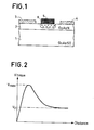
- Figure 2 shows this phenomenon, in which v o is the speed in equilibrium regime and v max is the maximum speed reached in ballistic regime.
- the speed v max can be 3 to 10 times the speed v o .
- the gate length is short enough for ballistic transport to take place, the transit time of the electrons under the gate is extremely short.
- the transistor then operates at a very high cut-off frequency or, for logic circuits, at very low switching times.
- Gridistor is known, the schematic section of which is shown in FIG. 3.
- N + type silicon substrate highly doped, is deposited a layer 8 in N type Si.
- Grids 9 are then implanted or diffused in layer 8.
- layers 10 are successively deposited.
- the P-type wells 12 are then implanted, which go around the transistor in order to connect the gates 9 to each other.
- Via metallizations 13 and 14, a current can be passed between source and drain. This current is modulated by the gate voltage. It can be noted that this current is not in the plane of the substrate.
- the Gridistor is said to have a vertical structure as opposed to the planar structure well known to those skilled in the art.
- US-A-3,999,281 Another field effect transistor, with vertical structure, is described by US-A-3,999,281. It is a MESFET. While in the Gridistor, the grid is produced by a semiconductor material P buried in a layer N, which complicates the production since epitaxy repeats are necessary, the MESFET described in patent US-A-3,999,281 comprises a metal grid deposited in the bottom of grooves dug in the layer N. The control of the current between source and drain is done by the electric field created inside the meshes of this metallic network. Nevertheless, the layer N, in which the grid acts, is important: it goes from the substrate (source or drain) to the metallization (drain or source) supported by the mesa formed between two grooves. So the grid length is important.
- the grid length is the distance traveled by the electrons under the grid.
- the length of the grid is therefore the thickness of the area 8 implanted or diffused.
- the structure of the Gridistor allows several grids to be placed in parallel, which is favorable for the production of a power device. But several factors mean that it is limited in operating frequency: the grid, of type P has a high resistance, the parasitic capacities created by the boxes 12 and the solder pads of the grids are very high and finally, the length of the grid hardly reaches a few thousand ⁇ ; which is insufficient to benefit from the ballistic transport phenomenon. In addition, a reduction in the grid length would cause a significant increase in its resistance. Finally, the layers 8 and 10 being of thickness greater than the gate length, there is created parasitic resistances of access R s and R D high.
- the transistors according to the invention have a vertical structure like the Gridistor but present significant progress as regards the operating frequencies, and a simplification of industrial production.
- the thickness of the active layer is small, of the order of several hundred angstroms, in order to be the seat of ballistic electron transport.
- the active layer is between two highly doped layers, themselves of small thickness, in order to minimize the access resistances R s and R ⁇ .
- the active layer is lightly doped, but because this layer is very thin and is between heavily doped layers, the concentration of electrons in the active layer is high, higher than the concentration of impurities .
- line 15 (in solid lines) represents the doping levels aimed theoretically in the structure N + NN +
- line 16 (in drawn lines) represents the real profile of the impurities taking into account the diffusion of these impurities between layers
- line 17 (dotted line) represents the real profile of the free electrons.
- the concentration of free electrons in the lightly doped N region is higher than that of doping impurities: the N region gains electrons at the expense of the N + regions .
- An N + NN + structure presents compared to a structure where the active layer N is intentionally doped at a level, for example, of 1 0 17 at.cm- 3 , not only the advantage of being the seat of ballistic transport but to facilitate the realization of the transistor.
- FIG. 5 represents, in schematic section, an example of a transistor according to the invention.
- a substrate 18 of heavily doped N + type GaAs are deposited successively by epitaxy a first layer 19 of N + type doped with some 10 18 at.cm- 3 thickness from 1000 to several thousand A, a second layer 20 of type N with an impurity concentration of approximately 10 15 at.cm- 3 and a thickness of several hundred ⁇ , and a third layer 21 of type N + doped with a thickness of approximately 1018 at.cm-3 from about 1000 A.
- a metallization 22 is deposited on the layer 21 to form a first ohmic contact, source or drain.
- the second contact, 23 drain or source is deposited on the other face of the substrate 18.
- a pad of lateral dimensions D equivalent to approximately twice the depth of the depressed areas is defined on the contact 22 plied with electrons 27.
- the depth of the depopulated areas 27 is approximately 1 micron.
- a dimension of 2 microns is very easily achievable by conventional lithography operations.
- the layer 21 is then removed except in the parts situated below the contact 22.
- the assembly is then attacked with a chemical solution so that the layer 21 is set back with respect to the contact 22, and that the layer 20 is partially attacked over about half of its thickness.
- a crystallographic orientation such that this chemical attack creates an inclined plane on the layer 20.
- the two wells 24 of high resistivity are obtained by bombardment of charged particles such as for example the protons, the central part being protected from the protons by the metallization 22.
- the two metallizations 25 of grid are then deposited by evaporation. This evaporation can be inclined relative to the normal to the plane of the substrate so that the metallizations 25 cover the side of the layer 20.
- the thickness of the metallizations must be less than that of the layer 20. In order to reduce the grid resistance, an excess thickness 26 of metallization is deposited on the grids.
- the modulation of the source-drain current is obtained by polarization of the grids 25, which varies the depth of the space charge zones 27. Because the thicknesses of the layers 20 and 25 are very small (a few hundred Angstroms) the distance traveled by the electrons under the grids is very small and the ballistic transport regime is obtained. This regime is all the easier to achieve when the concentration of impurities in the active layer 20 is low. On the other hand, the parasitic capacities are greatly reduced thanks to the boxes 24.
- This type of transistors finds its applications in the microwave domain, in particular for telecommunications.
Landscapes
- Engineering & Computer Science (AREA)
- Microelectronics & Electronic Packaging (AREA)
- Power Engineering (AREA)
- Physics & Mathematics (AREA)
- Ceramic Engineering (AREA)
- Condensed Matter Physics & Semiconductors (AREA)
- General Physics & Mathematics (AREA)
- Computer Hardware Design (AREA)
- Junction Field-Effect Transistors (AREA)
Description
La présente invention concerne les dispositifs à semi-conducteurs de type transistors à effet de champ, et plus spécialement ceux dont les grilles sont plus courtes que le libre parcours moyen des électrons dans le matériau semi-conducteur.The present invention relates to semiconductor devices of the field effect transistor type, and more particularly those whose gates are shorter than the mean free path of the electrons in the semiconductor material.
Les transistors à effet de champ connus fonctionnent soit selon une structure plane, le courant circulant dans le plan de la pastille de matériau semi-conducteur, soit selon une structure verticale, le courant circulant perpendiculairement à ce même plan.Known field effect transistors operate either according to a planar structure, the current flowing in the plane of the chip of semiconductor material, or according to a vertical structure, the current flowing perpendicular to this same plane.
Les transistors MESFET (de l'anglais Metal Schottky Field Effect Transistor), ayant une structure dite planar, possèdent sur la face libre de la plaquette les contacts ohmiques source et drain et le contact Schottky de grille. Les MESFET présentent de bonnes performances dans les domaines d'hyperfréquences ainsi que dans les circuits logiques. Cependant, afin d'améliorer leurs caractéristiques à très haute fréquence ou à très faible temps de commutation, il faut réduire la longueur de la grille jusqu'à des dimensions de 0,1 micron ou moins. Une telle réduction de la longueur de grille n'est pas aisée en technologie « planar », et est limitée par les techniques de masquage.The MESFET transistors (from the English Metal Schottky Field Effect Transistor), having a so-called planar structure, have the source and drain ohmic contacts and the gate Schottky contact on the free face of the wafer. MESFETs show good performance in the microwave domains as well as in logic circuits. However, in order to improve their characteristics at very high frequency or very low switching time, it is necessary to reduce the length of the grid to dimensions of 0.1 micron or less. Such a reduction in gate length is not easy in "planar" technology, and is limited by masking techniques.
Le Gridistor (Brevet Français n° 1 137 256 du 16 décembre 1961 et ses additions) est un transistor à effet de champ à jonction, à structure verticale possédant un grand nombre de grilles en parallèle. C'est donc un dispositif développant beaucoup de puissance. Mais sa fréquence de fonctionnement est basse en raison des capacités parasites élevées et d'une forte résistance de grille. De plus, par sa structure, plus la longueur de grille est faible, plus cette résistance est forte.The Gridistor (French Patent No. 1,137,256 of December 16, 1961 and its additions) is a junction field effect transistor with a vertical structure having a large number of gates in parallel. It is therefore a device developing a lot of power. However, its operating frequency is low due to the high stray capacitances and a high gate resistance. In addition, by its structure, the shorter the gate length, the stronger this resistance.
C'est pour pallier les inconvénients rencontrés dans les transistors communs de type MESFET et Gridistor, notamment en fréquence de fonctionnement, que de nouvelles structures de transitor à effet de champ ayant de très courtes longueurs de grille et de faibles résistances de grille et d'accès de source et de drain ont été mises au point.It is to overcome the drawbacks encountered in common transistors of the MESFET and Gridistor type, in particular in operating frequency, that new field effect transitor structures having very short gate lengths and low gate and source and drain accesses have been developed.
Les transistors à effet de champ selon l'invention fonctionnent selon une structure verticale, comparable à celle qui a été exposée au sujet du gridistor.The field effect transistors according to the invention operate according to a vertical structure, comparable to that which has been explained on the subject of the gridistor.
Cependant, la longueur de grille, dans les transistors selon l'invention est beaucoup plus faible que dans le Gridistor, parce que l'invention s'affranchit des grilles de type P incluses entre deux couches de type N par diffusion, soit une longueur de grille de l'ordre de la longueur de diffusion.However, the gate length, in the transistors according to the invention is much shorter than in the Gridistor, because the invention overcomes the P type gates included between two N type layers by diffusion, i.e. a length of grid of the order of the diffusion length.
La longueur de grille, dans l'invention, est limitée à une épaisseur de couche épitaxiale, que l'on sait réaliser très mince, de l'ordre de quelques centaines d'angstrôms, et l'effet de grille, par pincement d'une zone dépeuplée en électrons, est obtenue par une métallisation, située dans le plan de la couche de grille mais latéralement, en contact électrique avec elle, et qui permet d'appliquer la tension de contrôle de grille.The length of the grid, in the invention, is limited to a thickness of epitaxial layer, which is known to be very thin, of the order of a few hundred angstroms, and the grid effect, by pinching an area depopulated with electrons, is obtained by metallization, located in the plane of the gate layer but laterally, in electrical contact with it, and which makes it possible to apply the gate control voltage.
De façon plus précise, l'invention concerne un transistor à effet de champ, à grille ultracourte, tel qu'énoncé dans la revendication 1.More specifically, the invention relates to a field effect transistor, with an ultra-short gate, as set out in
L'invention sera mieux comprise par la description d'un exemple de réalisation, laquelle s'appuie sur des figures parmi lesquelles :
- La figure 1 représente une coupe schématique d'un MESFET selon l'art connu ;
- La figure 2 représente le diagramme de variation de la vitesse des électrons en fonction de la distance parcourue, dans un matériau semi-conducteur ;
- La figure 3 représente une coupe schématique d'un Gridistor selon l'art connu ;
- La figure 4 représente la répartition de la concentration en électrons dans une structure multicouche où la couche centrale faiblement dopée est intercalée entre deux couches fortement dopées ;
- La figure 5 représente en coupe schématique, un exemple de transistor à grille ultracourte selon l'invention.
- La figure 1 représente la coupe schématique d'un transistor MESFET selon l'art connu : de façon à se rapprocher du domaine de l'invention, celui des hyperfréquences, le matériau choisi pour cet exemple est parmi d'autres possibles, l'arséniure de gallium.
- Figure 1 shows a schematic section of a MESFET according to the known art;
- FIG. 2 represents the diagram of variation of the speed of the electrons as a function of the distance traveled, in a semiconductor material;
- Figure 3 shows a schematic section of a Gridistor according to known art;
- FIG. 4 represents the distribution of the electron concentration in a multilayer structure where the weakly doped central layer is interposed between two strongly doped layers;
- FIG. 5 represents in schematic section, an example of an ultra-short gate transistor according to the invention.
- FIG. 1 represents the schematic section of a MESFET transistor according to the known art: in order to approach the field of the invention, that of microwaves, the material chosen for this example is among other possible, arsenide of gallium.
Sur un substrat 1 en GaAs semi-isolant est déposée une couche 2 en GaAs de type N. Les contacts ohmiques 3 de source et 4 de drain sont déposés par métallisation. Par l'intermédiaire de la grille 5, soumise à une tension de contrôle, se développe une région de charge d'espace 6 dont l'épaisseur dépend de la tension grille. Le courant source-drain est donc modulé par la tension grille. La strcture est dite planar.A
La fréquence de fonctionnement ou le temps de commutation de ce type de transistor, dépend du temps de transit des électrons sous la grille. Or ce temps de transit est d'autant plus faible que la grille est plus courte. Il est donc avantageux de réduire la longueur de la grille. Cette réduction est d'autant plus intéressante que, pour de très courtes longueurs de grille (quelques centaines d'A à quelques milliers d'À selon le dopage du matériau) un phénomène physique, appelé transport balistique, doit être pris en compte.The operating frequency or the switching time of this type of transistor depends on the transit time of the electrons under the gate. However, this transit time is lower the shorter the grid. It is therefore advantageous to reduce the length of the grid. This reduction is all the more interesting since, for very short gate lengths (a few hundred A to a few thousand A depending on the doping of the material) a physical phenomenon, called ballistic transport, must be taken into account.
Le transport balistique des électrons peut se décrire succintement comme suit : on peut définir pour un électron, en déplacement sous un champ électrique, un libre parcours moyen tenant compte des collisions de cet électron dans le réseau cristallin : collision avec les impuretés, avec les phonons, etc... Lorsque la distance parcourue par l'électron est plus faible que le libre parcours moyen, l'électron atteint une vitesse maximale, supérieure à celle qu'il possède après collisions, car à chaque collision il perd de l'énergie.The ballistic transport of electrons can be described briefly as follows: we can define for an electron, moving under an electric field, an average free path taking into account the collisions of this electron in the crystal lattice: collision with impurities, with phonons , etc ... When the distance traveled by the electron is shorter than the average free path, the electron reaches a maximum speed, higher than that which it has after collisions, because with each collision it loses energy .
La figure 2 représente ce phénomène, dans lequel vo est la vitesse en régime d'équilibre et vmax est la vitesse maximale atteinte en régime balistique. Selon le champ électrique appliqué, la vitesse vmax peut être de 3 à 10 fois la vitesse vo. En d'autres termes, lorsque la longueur de grille est suffisamment faible pour que le transport balistique ait lieu, le temps de transit des électrons sous la grille est extrêmement court. Le transistor fonctionne alors à très haute fréquence de coupure ou, pour les circuits logiques, à de très faibles temps de commutation.Figure 2 shows this phenomenon, in which v o is the speed in equilibrium regime and v max is the maximum speed reached in ballistic regime. Depending on the applied electric field, the speed v max can be 3 to 10 times the speed v o . In other words, when the gate length is short enough for ballistic transport to take place, the transit time of the electrons under the gate is extremely short. The transistor then operates at a very high cut-off frequency or, for logic circuits, at very low switching times.
Il est donc utile de réduire la longueur de grille des MESFET jusqu'à des dimensions voisines de 0,1 micron, mais ceci nécessite une technologie assez lourde, et il est difficile d'envisager, des dimensions inférieures à 0,1 micron, au stade de l'art actuel de la technologie planar.It is therefore useful to reduce the grid length of the MESFETs to dimensions close to 0.1 micron, but this requires fairly heavy technology, and it is difficult to envisage, dimensions smaller than 0.1 micron, at the current state of the art of planar technology.
D'autre part on connaît le Gridistor dont la coupe schématique est représentée sur la figure 3.On the other hand, the Gridistor is known, the schematic section of which is shown in FIG. 3.
Sur un subtrat 7 en silicium de type N+, fortement dopé, est déposée une couche 8 en Si de type N. On implante ou diffuse alors dans la couche 8, des grilles 9 de type P. On dépose ensuite successivement les couches 10 de type N et 11 de type N+. On implante ensuite les caissons 12 de type P, qui font le tour du transistor afin de relier les grilles 9 entre elles. Par l'intermédiaire des métallisations 13 et 14 on peut faire passer un courant entre source et drain. Ce courant est modulé par la tension grille. On peut remarquer que ce courant n'est pas dans le plan du substrat. Le Gridistor est dit de structure verticale par opposition avec la structure planar bien connue de l'homme de l'art.On a N + type silicon substrate, highly doped, is deposited a layer 8 in N type Si.
Un autre transistor à effet de champ, à structure verticale, est décrit par le brevet US-A-3 999 281. Il s'agit d'un MESFET. Alors que dans le Gridistor, la grille est réalisée par un matériau semi-conducteur P enterré dans une couche N, ce qui complique la réalisation puisque des reprises d'épitaxie sont nécessaires, le MESFET décrit dans le brevet US-A-3 999 281 comporte une grille métallique déposée dans le fond de sillons creusés dans la couche N. Le contrôle du courant entre source et drain se fait par le champ électrique créé à l'intérieur des mailles de ce réseau métallique. Néanmoins, la couche N, dans laquelle la grille agit, est importante : elle va depuis le substrat (source ou drain) jusqu'à la métallisation (drain ou source) supportée par le mésa formé entre deux sillons. Ainsi, la longueur de grille est importante.Another field effect transistor, with vertical structure, is described by US-A-3,999,281. It is a MESFET. While in the Gridistor, the grid is produced by a semiconductor material P buried in a layer N, which complicates the production since epitaxy repeats are necessary, the MESFET described in patent US-A-3,999,281 comprises a metal grid deposited in the bottom of grooves dug in the layer N. The control of the current between source and drain is done by the electric field created inside the meshes of this metallic network. Nevertheless, the layer N, in which the grid acts, is important: it goes from the substrate (source or drain) to the metallization (drain or source) supported by the mesa formed between two grooves. So the grid length is important.
Par convention on définit la longueur de grille comme la distance parcourue par les électrons sous la grille. Dans le cas du Gridistor la longueur de grille est donc l'épaisseur de la zone 8 implantée ou diffusée. Par ailleurs la structure du Gridistor permet de mettre en parallèle plusieurs grilles, ce qui est favorable à la réalisation d'un dispositif de puissance. Mais plusieurs facteurs font qu'il est limité en fréquence de fonctionnement : la grille, de type P présente une grande résistance, les capacités parasites créées par les caissons 12 et les plots de soudure des grilles sont très élevées et enfin, la longueur de grille atteint difficilement quelques milliers d'Å ; ce qui est insuffisant pour bénéficier du phénomène de transport balistique. De plus, une réduction de la longueur de grille provoquerait une augmentation notable de sa résistance. Enfin, les couches 8 et 10 étant d'épaisseur supérieure à la longueur de grille, il s'y crée des résistances parasites d'accès Rs et RD élevées.By convention we define the grid length as the distance traveled by the electrons under the grid. In the case of the Gridistor, the length of the grid is therefore the thickness of the area 8 implanted or diffused. Furthermore, the structure of the Gridistor allows several grids to be placed in parallel, which is favorable for the production of a power device. But several factors mean that it is limited in operating frequency: the grid, of type P has a high resistance, the parasitic capacities created by the
Les transistors selon l'invention, ont une structure verticale comme le Gridistor mais présentent d'importants progrès en ce qui concerne les fréquences du fonctionnement, et une simplification de réalisation industrielle.The transistors according to the invention have a vertical structure like the Gridistor but present significant progress as regards the operating frequencies, and a simplification of industrial production.
En premier lieu, l'épaisseur de la couche active est faible, de l'ordre de plusieurs centaines d'angstrôms, afin d'être le siège du transport balistique d'électrons.First, the thickness of the active layer is small, of the order of several hundred angstroms, in order to be the seat of ballistic electron transport.
En second lieu, la couche active est comprise entre deux couches fortement dopées, elles- mêmes de faible épaisseur, afin de minimiser les résistances d'accès Rs et Rε.Secondly, the active layer is between two highly doped layers, themselves of small thickness, in order to minimize the access resistances R s and Rε.
En troisième lieu, la couche active est faiblement dopée, mais du fait que cette couche est très mince et qu'elle est comprise entre des couches fortement dopées, la concentration en électrons dans la couche active est élevée, plus élevée que la concentration en impuretés.Third, the active layer is lightly doped, but because this layer is very thin and is between heavily doped layers, the concentration of electrons in the active layer is high, higher than the concentration of impurities .
Cette propriété est décrite sur la figure 4 : la ligne 15 (en trait plein) représente les niveaux de dopage visés théoriquement dans la structure N+NN+, la ligne 16 (en traits tirés) représente le profil réel des impuretés compte tenu de la diffusion de ces impuretés entre couches, et la ligne 17 (en pointillé) représente le profil réel des électrons libres. La concentration en électrons libres dans la région N peu dopée est plus forte que celle des impuretés dopants : la région N gagne des électrons au dépend des régions N+. Une structure N+NN+ présente par rapport à une structure où la couche active N est intentionnellement dopée à un niveau, par exemple, de 10 17 at.cm-3, non seulement l'avantage d'être le siège du transport balistique mais de faciliter la réalisation du transistor.This property is described in FIG. 4: line 15 (in solid lines) represents the doping levels aimed theoretically in the structure N + NN + , line 16 (in drawn lines) represents the real profile of the impurities taking into account the diffusion of these impurities between layers, and line 17 (dotted line) represents the real profile of the free electrons. The concentration of free electrons in the lightly doped N region is higher than that of doping impurities: the N region gains electrons at the expense of the N + regions . An N + NN + structure presents compared to a structure where the active layer N is intentionally doped at a level, for example, of 1 0 17 at.cm- 3 , not only the advantage of being the seat of ballistic transport but to facilitate the realization of the transistor.
La figure 5 représente, en coupe schématique, un exemple de transistor selon l'invention.FIG. 5 represents, in schematic section, an example of a transistor according to the invention.
Sur un substrat 18 en GaAs de type N+ fortement dopé sont déposées successivement par épitaxie une première couche 19 de type N+ dopée à quelques 1018 at.cm-3 d'épaisseur de 1 000 à plusieurs milliers d'A, une seconde couche 20 de type N de concentration en impuretés d'environ 1015 at.cm-3 et d'épaisseur de plusieurs centaines d'Â, et une troisième couche 21 de type N+ dopée à quelques 1018 at.cm-3 d'épaisseur de 1 000 A environ. Une métallisation 22 est déposée sur la couche 21 pour constituer un premier contact ohmique, source ou drain. Le second contact, 23 drain ou source, est déposé sur l'autre face du substrat 18.On a
Par opération de lithographie connue de l'homme de l'art, on définit sur le contact 22 un plot de dimensions latérales D équivalentes à environ deux fois la profondeur des zones dépeuplées d'électrons 27. Pour un dopage 1015 at.cm-3, la profondeur des zones dépeuplées 27 est de 1 micron environ. Une dimension de 2 microns est très facilement réalisable par les opérations de lithographie classique.By lithography operation known to those skilled in the art, a pad of lateral dimensions D equivalent to approximately twice the depth of the depressed areas is defined on the
Par gravure ionique on enlève ensuite la couche 21 sauf dans les parties situées en dessous du contact 22. On attaque ensuite l'ensemble avec une solution chimique de telle façon que la couche 21 soit en retrait par rapport au contact 22, et que la couche 20 soit partiellement attaquée sur la moitié de son épaisseur environ. On peut choisir une orientation cristallographique telle que cette attaque chimique crée un plan incliné sur la couche 20. Les deux caissons 24 de haute résistivité sont obtenus par bombardement de particules chargées telles que par exemple les protons, la partie centrale étant protégée des protons par la métallisation 22. On dépose ensuite les deux métallisations 25 de grille par évaporation. Cette évaporation peut être inclinée par rapport à la normale au plan du substrat de façon à ce que les métallisations 25 recouvrent le flanc de la couche 20. L'épaisseur des métallisations doit être plus faible que celle de la couche 20. Afin de réduire la résistance de grille, on dépose une surépaisseur 26 de métallisation sur les grilles.By ion etching, the
La modulation du courant source-drain est obtenue par polarisation des grilles 25, qui fait varier la profondeur des zones de charge d'espace 27. Du fait que les épaisseurs des couches 20 et 25 sont très faibles (quelques centaines d'Angstrôms) la distance parcourue par les électrons sous les grilles est très faible et le régime de transport balistique est obtenu. Ce régime est d'autant plus facile à atteindre que la concentration en impuretés dans la couche active 20 est faible. D'autre part, les capacités parasites sont fortement diminuées grâce aux caissons 24.The modulation of the source-drain current is obtained by polarization of the grids 25, which varies the depth of the space charge zones 27. Because the thicknesses of the
Afin de mieux contrôler les profils d'impuretés dans la structure N+NN+ on peut intercaler entre les couches 19 et 20 et les couches 20 et 21 une couche mince d'épaisseur de l'ordre de quelques centaines d'angstrôms et de dopage de l'ordre de 1017 at.cm-3. In order to better control the impurity profiles in the N + NN + structure, it is possible to interpose between
Ce type de transistors plus particulièrement réalisé avec des matériaux du type GaAs et de la famille III-V, trouve ses applications dans le domaine des hyperfréquences, notamment pour les télécommunications.This type of transistors, more particularly produced with materials of the GaAs type and of the III-V family, finds its applications in the microwave domain, in particular for telecommunications.
Claims (5)
Applications Claiming Priority (2)
| Application Number | Priority Date | Filing Date | Title |
|---|---|---|---|
| FR8023385 | 1980-10-31 | ||
| FR8023385A FR2493604A1 (en) | 1980-10-31 | 1980-10-31 | ULTRA SHORT GRID FIELD EFFECT TRANSISTORS |
Publications (2)
| Publication Number | Publication Date |
|---|---|
| EP0051504A1 EP0051504A1 (en) | 1982-05-12 |
| EP0051504B1 true EP0051504B1 (en) | 1983-12-28 |
Family
ID=9247566
Family Applications (1)
| Application Number | Title | Priority Date | Filing Date |
|---|---|---|---|
| EP81401504A Expired EP0051504B1 (en) | 1980-10-31 | 1981-09-29 | Field effect transistor having a short channel |
Country Status (6)
| Country | Link |
|---|---|
| US (1) | US4768071A (en) |
| EP (1) | EP0051504B1 (en) |
| JP (1) | JPS57104268A (en) |
| CA (1) | CA1168763A (en) |
| DE (1) | DE3161796D1 (en) |
| FR (1) | FR2493604A1 (en) |
Families Citing this family (15)
| Publication number | Priority date | Publication date | Assignee | Title |
|---|---|---|---|---|
| FR2520157B1 (en) * | 1982-01-18 | 1985-09-13 | Labo Electronique Physique | SEMICONDUCTOR DEVICE OF THE HETEROJUNCTION TRANSISTOR TYPE (S) |
| JPS58173870A (en) * | 1982-04-05 | 1983-10-12 | インタ−ナシヨナル ビジネス マシ−ンズ コ−ポレ−シヨン | Semiconductor device |
| US4587540A (en) * | 1982-04-05 | 1986-05-06 | International Business Machines Corporation | Vertical MESFET with mesa step defining gate length |
| JPS5982772A (en) * | 1982-11-02 | 1984-05-12 | Nippon Telegr & Teleph Corp <Ntt> | Manufacture of field effect transistor |
| FR2548454B1 (en) * | 1983-07-01 | 1986-12-12 | Labo Electronique Physique | FIELD EFFECT TRANSISTOR WITH SUBMICRON GRID HAVING VERTICAL STRUCTURE |
| FR2555816B1 (en) * | 1983-11-25 | 1986-04-11 | Thomson Csf | VERTICAL STRUCTURE FIELD EFFECT TRANSISTOR |
| FR2557368B1 (en) * | 1983-12-27 | 1986-04-11 | Thomson Csf | FIELD EFFECT TRANSISTOR, WITH SUBMICRON VERTICAL STRUCTURE, AND METHOD FOR PRODUCING THE SAME |
| GB2162370B (en) * | 1984-07-26 | 1987-10-28 | Japan Res Dev Corp | Static induction transistor and integrated circuit comprising such a transistor |
| DE3535002A1 (en) * | 1985-10-01 | 1987-04-02 | Telefunken Electronic Gmbh | BARRIER LAYER EFFECT TRANSISTOR |
| DE3789894T2 (en) * | 1987-01-05 | 1994-09-08 | Seiko Instr Inc | MOS field effect transistor and its manufacturing method. |
| US5923985A (en) * | 1987-01-05 | 1999-07-13 | Seiko Instruments Inc. | MOS field effect transistor and its manufacturing method |
| US5219772A (en) * | 1991-08-15 | 1993-06-15 | At&T Bell Laboratories | Method for making field effect devices with ultra-short gates |
| KR950034830A (en) * | 1994-04-29 | 1995-12-28 | 빈센트 비. 인그라시아 | Field effect transistor and method of manufacturing the transistor |
| JP3368799B2 (en) * | 1997-05-22 | 2003-01-20 | 住友電気工業株式会社 | III-V compound semiconductor wafer and method of manufacturing the same |
| JP5087818B2 (en) * | 2005-03-25 | 2012-12-05 | 日亜化学工業株式会社 | Field effect transistor |
Family Cites Families (6)
| Publication number | Priority date | Publication date | Assignee | Title |
|---|---|---|---|---|
| US3660180A (en) * | 1969-02-27 | 1972-05-02 | Ibm | Constrainment of autodoping in epitaxial deposition |
| US3761785A (en) * | 1971-04-23 | 1973-09-25 | Bell Telephone Labor Inc | Methods for making transistor structures |
| US3999281A (en) * | 1976-01-16 | 1976-12-28 | The United States Of America As Represented By The Secretary Of The Air Force | Method for fabricating a gridded Schottky barrier field effect transistor |
| US4129879A (en) * | 1977-04-21 | 1978-12-12 | General Electric Company | Vertical field effect transistor |
| US4343015A (en) * | 1980-05-14 | 1982-08-03 | General Electric Company | Vertical channel field effect transistor |
| US4366493A (en) * | 1980-06-20 | 1982-12-28 | International Business Machines Corporation | Semiconductor ballistic transport device |
-
1980
- 1980-10-31 FR FR8023385A patent/FR2493604A1/en active Granted
-
1981
- 1981-09-29 EP EP81401504A patent/EP0051504B1/en not_active Expired
- 1981-09-29 DE DE8181401504T patent/DE3161796D1/en not_active Expired
- 1981-10-13 US US06/312,258 patent/US4768071A/en not_active Expired - Fee Related
- 1981-10-27 CA CA000388883A patent/CA1168763A/en not_active Expired
- 1981-10-30 JP JP56173132A patent/JPS57104268A/en active Pending
Also Published As
| Publication number | Publication date |
|---|---|
| US4768071A (en) | 1988-08-30 |
| JPS57104268A (en) | 1982-06-29 |
| FR2493604A1 (en) | 1982-05-07 |
| CA1168763A (en) | 1984-06-05 |
| EP0051504A1 (en) | 1982-05-12 |
| DE3161796D1 (en) | 1984-02-02 |
| FR2493604B1 (en) | 1982-11-26 |
Similar Documents
| Publication | Publication Date | Title |
|---|---|---|
| EP0017531B1 (en) | Field-effect transistor with high cut-off frequency and method of making it | |
| EP0051504B1 (en) | Field effect transistor having a short channel | |
| KR100647173B1 (en) | Novel field effect transistor and method of fabrication | |
| US20190051649A1 (en) | Semiconductor device and manufacturing method of the same | |
| EP3203526B1 (en) | Heterojunction transistor with improved electron gas confinement | |
| EP0025742B1 (en) | Field-effect transistor having a high cut-off frequency | |
| JPS6313355B2 (en) | ||
| EP2680311A1 (en) | Tunnel-effect transistor | |
| FR2593966A1 (en) | MONOLITHIC SEMICONDUCTOR STRUCTURE OF A BIPOLAR HETEROJUNCTION TRANSISTOR AND A LASER | |
| FR3011981A1 (en) | HETEROJUNCTION-BASED HEMT TRANSISTOR | |
| WO1981000175A1 (en) | Floating gate vertical fet | |
| EP0046422B1 (en) | Gaas field-effect transistor with non volatile memory | |
| FR2508707A1 (en) | BALLISTIC TRANSISTOR WITH MULTIPLE HETEROJUNCTIONS | |
| EP0145567B1 (en) | Field-effect transistor having a vertical structure | |
| EP0522952B1 (en) | Field effect transistor with thin barrier layers and a thin doped layer | |
| FR2496990A1 (en) | SCHOTTKY BARRIER FIELD EFFECT TRANSISTOR | |
| EP0503731B1 (en) | Method of making a transistor with high electron mobility | |
| EP0149390A2 (en) | Field effect transistor with a vertical sub-micronic structure and process for its production | |
| FR2497603A1 (en) | TRANSISTOR WITH LOW SWITCHING TIME OF NORMALLY BLOCKING TYPE | |
| WO2019224448A1 (en) | Enhancement-mode high-electron-mobility transistor | |
| FR2700221A1 (en) | Field effect transistor having improved stray capacitance and transconductance properties. | |
| US5219772A (en) | Method for making field effect devices with ultra-short gates | |
| EP0027761B1 (en) | High-frequency field effect semiconductor device and transistor using such a semiconductor device | |
| FR2604828A1 (en) | METHOD FOR MANUFACTURING A P + NN + DIODE AND A BIPOLAR TRANSISTOR HAVING THE SAME, USING THE NEUTRALIZATION EFFECT OF DONOR ATOMS BY ATOMIC HYDROGEN | |
| JP2701583B2 (en) | Tunnel transistor and manufacturing method thereof |
Legal Events
| Date | Code | Title | Description |
|---|---|---|---|
| PUAI | Public reference made under article 153(3) epc to a published international application that has entered the european phase |
Free format text: ORIGINAL CODE: 0009012 |
|
| AK | Designated contracting states |
Designated state(s): DE GB IT NL |
|
| 17P | Request for examination filed |
Effective date: 19820608 |
|
| ITF | It: translation for a ep patent filed | ||
| GRAA | (expected) grant |
Free format text: ORIGINAL CODE: 0009210 |
|
| AK | Designated contracting states |
Designated state(s): DE GB IT NL |
|
| REF | Corresponds to: |
Ref document number: 3161796 Country of ref document: DE Date of ref document: 19840202 |
|
| PGFP | Annual fee paid to national office [announced via postgrant information from national office to epo] |
Ref country code: DE Payment date: 19840723 Year of fee payment: 4 |
|
| PLBE | No opposition filed within time limit |
Free format text: ORIGINAL CODE: 0009261 |
|
| STAA | Information on the status of an ep patent application or granted ep patent |
Free format text: STATUS: NO OPPOSITION FILED WITHIN TIME LIMIT |
|
| 26N | No opposition filed | ||
| PGFP | Annual fee paid to national office [announced via postgrant information from national office to epo] |
Ref country code: NL Payment date: 19860930 Year of fee payment: 6 |
|
| PG25 | Lapsed in a contracting state [announced via postgrant information from national office to epo] |
Ref country code: NL Effective date: 19880401 |
|
| NLV4 | Nl: lapsed or anulled due to non-payment of the annual fee | ||
| PG25 | Lapsed in a contracting state [announced via postgrant information from national office to epo] |
Ref country code: DE Effective date: 19880601 |
|
| GBPC | Gb: european patent ceased through non-payment of renewal fee | ||
| PG25 | Lapsed in a contracting state [announced via postgrant information from national office to epo] |
Ref country code: GB Free format text: LAPSE BECAUSE OF NON-PAYMENT OF DUE FEES Effective date: 19881118 |