EP0049990B1 - Folded bit line-shared sense amplifiers - Google Patents
Folded bit line-shared sense amplifiers Download PDFInfo
- Publication number
- EP0049990B1 EP0049990B1 EP81304614A EP81304614A EP0049990B1 EP 0049990 B1 EP0049990 B1 EP 0049990B1 EP 81304614 A EP81304614 A EP 81304614A EP 81304614 A EP81304614 A EP 81304614A EP 0049990 B1 EP0049990 B1 EP 0049990B1
- Authority
- EP
- European Patent Office
- Prior art keywords
- pair
- coupled
- node
- transistor
- bit lines
- Prior art date
- Legal status (The legal status is an assumption and is not a legal conclusion. Google has not performed a legal analysis and makes no representation as to the accuracy of the status listed.)
- Expired
Links
- 230000015654 memory Effects 0.000 claims description 99
- 239000003990 capacitor Substances 0.000 claims description 39
- 238000002955 isolation Methods 0.000 claims description 30
- 230000008878 coupling Effects 0.000 claims description 11
- 238000010168 coupling process Methods 0.000 claims description 11
- 238000005859 coupling reaction Methods 0.000 claims description 11
- 238000000034 method Methods 0.000 claims description 6
- 230000003213 activating effect Effects 0.000 claims description 4
- 230000001143 conditioned effect Effects 0.000 claims description 4
- 230000000295 complement effect Effects 0.000 claims 1
- 230000007704 transition Effects 0.000 description 2
- 230000008901 benefit Effects 0.000 description 1
- 238000010276 construction Methods 0.000 description 1
- 238000010586 diagram Methods 0.000 description 1
- 239000011159 matrix material Substances 0.000 description 1
- 230000002093 peripheral effect Effects 0.000 description 1
- 230000001105 regulatory effect Effects 0.000 description 1
- 230000004044 response Effects 0.000 description 1
- 239000004065 semiconductor Substances 0.000 description 1
Images
Classifications
-
- G—PHYSICS
- G11—INFORMATION STORAGE
- G11C—STATIC STORES
- G11C11/00—Digital stores characterised by the use of particular electric or magnetic storage elements; Storage elements therefor
- G11C11/21—Digital stores characterised by the use of particular electric or magnetic storage elements; Storage elements therefor using electric elements
- G11C11/34—Digital stores characterised by the use of particular electric or magnetic storage elements; Storage elements therefor using electric elements using semiconductor devices
- G11C11/40—Digital stores characterised by the use of particular electric or magnetic storage elements; Storage elements therefor using electric elements using semiconductor devices using transistors
- G11C11/401—Digital stores characterised by the use of particular electric or magnetic storage elements; Storage elements therefor using electric elements using semiconductor devices using transistors forming cells needing refreshing or charge regeneration, i.e. dynamic cells
- G11C11/4063—Auxiliary circuits, e.g. for addressing, decoding, driving, writing, sensing or timing
- G11C11/407—Auxiliary circuits, e.g. for addressing, decoding, driving, writing, sensing or timing for memory cells of the field-effect type
- G11C11/409—Read-write [R-W] circuits
- G11C11/4097—Bit-line organisation, e.g. bit-line layout, folded bit lines
-
- G—PHYSICS
- G11—INFORMATION STORAGE
- G11C—STATIC STORES
- G11C11/00—Digital stores characterised by the use of particular electric or magnetic storage elements; Storage elements therefor
- G11C11/21—Digital stores characterised by the use of particular electric or magnetic storage elements; Storage elements therefor using electric elements
- G11C11/34—Digital stores characterised by the use of particular electric or magnetic storage elements; Storage elements therefor using electric elements using semiconductor devices
- G11C11/40—Digital stores characterised by the use of particular electric or magnetic storage elements; Storage elements therefor using electric elements using semiconductor devices using transistors
- G11C11/401—Digital stores characterised by the use of particular electric or magnetic storage elements; Storage elements therefor using electric elements using semiconductor devices using transistors forming cells needing refreshing or charge regeneration, i.e. dynamic cells
- G11C11/4063—Auxiliary circuits, e.g. for addressing, decoding, driving, writing, sensing or timing
- G11C11/407—Auxiliary circuits, e.g. for addressing, decoding, driving, writing, sensing or timing for memory cells of the field-effect type
- G11C11/409—Read-write [R-W] circuits
-
- G—PHYSICS
- G11—INFORMATION STORAGE
- G11C—STATIC STORES
- G11C11/00—Digital stores characterised by the use of particular electric or magnetic storage elements; Storage elements therefor
- G11C11/21—Digital stores characterised by the use of particular electric or magnetic storage elements; Storage elements therefor using electric elements
- G11C11/34—Digital stores characterised by the use of particular electric or magnetic storage elements; Storage elements therefor using electric elements using semiconductor devices
- G11C11/40—Digital stores characterised by the use of particular electric or magnetic storage elements; Storage elements therefor using electric elements using semiconductor devices using transistors
- G11C11/401—Digital stores characterised by the use of particular electric or magnetic storage elements; Storage elements therefor using electric elements using semiconductor devices using transistors forming cells needing refreshing or charge regeneration, i.e. dynamic cells
- G11C11/4063—Auxiliary circuits, e.g. for addressing, decoding, driving, writing, sensing or timing
- G11C11/407—Auxiliary circuits, e.g. for addressing, decoding, driving, writing, sensing or timing for memory cells of the field-effect type
- G11C11/409—Read-write [R-W] circuits
- G11C11/4091—Sense or sense/refresh amplifiers, or associated sense circuitry, e.g. for coupled bit-line precharging, equalising or isolating
Definitions
- the present invention relates generally to improvements in MOS (metal-oxide- semiconductor) memories and, more particularly, to a shared sense amplifier arrangement for sensing the logic state of a memory cell.
- MOS metal-oxide- semiconductor
- each cell includes a capacitor for storing a charge which indicates whether its cell is in a logic 1 or a logic 0 state.
- a large number of such memory cells are typically associated with each of the memory's bit lines.
- a number of dummy cells are also included in the memory. These dummy cells have dummy capacitors which are precharged to reference voltage levels.
- the charge of the memory's cell capacitor is dumped on a first bit line and the charge on the dummy cell's capacitor is dumped on a second bit line.
- The-resultant difference in voltage on the two bit lines is sensed by a sense amplifier and used as an indication of whether the memory cell is in a logic 1 or a logic 0 state.
- a sense amplifier is typically positioned between and coupled to two pairs of bit lines.
- Such an arrangement is shown in DE-A-2 919 166 (Fig. 7, 8) in which the sense amplifier is constructed to sense the voltage difference between the two bit lines of the pair of one or the other side of the sense amplifier.
- respective, input/output lines have to be provided to each side of the sense amplifier together with appropriate decoders such that the arrangement is complex, difficult to read, and occupies a large area.
- bit lines on one side of the sense amplifier are typically coupled to input/output buss lines, the latter bit lines are used as conductive paths for coupling the latched state of the sense amplifier to the input/output buss lines._ This facility for easily reading the latched stated of the sense amplifier is a prime reason for the above-mentioned arrangement.
- an MOS memory comprising a plurality of memory cells each having a memory cell capacitor adapted to be charged so as to reflect the logic state of its memory cell, a plurality of bit lines and word lies for accessing a particular memory cell input/output buss lines for reading the logic state of the accessed memory cell, and a folded bit line-shared sense amplifier arrangement for sensing the state of an access memory cell, said sense amplifier arrangement comprising a first pair of bit lines which are adjacent to each other and are coupled to respective first and second input-output modes of said shared sense amplifier by a respective one of a first pair of isolation transistors, a second pair of bit lines which are adjacent to each other and are coupled to said respective first and second input- output modes of said shared sense amplifier by a respective one of a second pair of isolation transistors the first pair of bit lines being located on one side, the second pair at the other side of the shared sense amplifier on the chip, and decoding means for activating a selected pair of isolation transistors to couple the associated pair of bit lines
- the shared sense amplifier arrangement of the MOS memory of the invention provides good common mode noise rejection while simultaneously enabling the latched state of the sense amplifier to be read by the input/output buss lines.
- the invention also extends to a method of reading the logic state of an accessed memory cell in an MOS memory, wherein said memory comprises a plurality of memory cells each having a memory cell capacitor adapted to be charged so as to reflect the logic state of its memory cell, a plurality of bit lines and word lines for accessing a particular memory cell, input/ output buss lines for reading the logic state of the accessed memory cell, and a folded bit line-shared sense amplifier arrangement for sensing the state of an accessed memory cell, said sense amplifier arrangement comprising a first pair of bit lines which are adjacent to each other and are coupled to respective first and second input- output modes of said shared sense amplifier by a respective one of a first pair of isolation transistors, a second pair of bit lines which are adjacent to each other and are coupled to said respective first and second input-output modes of said shared sense amplifier by a respective one of a second pair of isolation transistors the first pair of bit lines being located on one side, the second pair at the other side of the shared sense amplifier on the chip, and wherein said method comprises
- a representative portion of a dynamic MOS memory which includes a preferred embodiment of a sense amplifier arrangement.
- the illustrated portion has four pairs of bit lines identified as A-B, C-D, E-F, and G-H.
- the pair of bit lines A-B is coupled through isolation transistors 10 and 12 to a sense amplifier 14.
- the pair of bit lines C-D is similarly coupled to the sense amplifier 14 via isolation transistors 16 and 18.
- the sense amplifier 14 is adapted by decoding circuitry to sense the potentials on bit lines A and B or on bit lines C and D.
- the pairs of bit lines E-F and G-H are similarly connected to another sense amplifier 20.
- one of the bit lines for each pair is coupled to a capacitor associated with an addressed memory cell so that a charge transfer occurs between that bit line and the latter capacitor.
- the other bit line in that pair (B, for example) carries a reference voltage induced by a dummy cell capacitor.
- the sense amplifier detects the voltage difference between bit lines A and B and latches in a state representing this difference. The latched state of the sense amplifier therefore represents the logic level of the addressed memory cell.
- the decoding circuitry enables the data on the bit lines A and B to be coupled to input/output (I/O andTTO) buss lines 17 and 19 via bit lines C and D.
- I/O andTTO input/output
- bit line D is coupled to the I/O buss 19 via a transistor DT, the state of the sense amplifier is readily ascertained.
- bit line D provides a path for sensing the state of the amplifier 14.
- Bit lines B and C are used in the same manner.
- bit lines A and B are usually physically close to each other, as are bit lines C and D.
- bit lines A and D are physically separated from each other on the memory chip.
- any noise which affects bit line A will probably not influence bit line D in the same manner.
- the conventional sense amplifier arrangement senses bit lines having different amounts of noise and is therefore, susceptible to developing noise- induced errors. Because the present arrangement senses bit lines which are physically near each other on the chip, noise problems are reduced.
- switch circuitry described below permits the state of the sense amplifiers to be conveniently transferred to the t/0 and I/O busses.
- this device includes transistors 22 and 24 which are interconnected as a flip-flop with voltage nodes 21 and 23. As shown, terminal 10a of the transistor 10 is coupled to the drain of the transistor 22 and to the gate of the transistor 24. Terminal 12a of the transistor 12 is coupled to the drain of the transistor 24 and to the gate of the transistor 22.
- the sense amplifier is coupled to a latching transistor 25 whose gate is driven by clock signal 0 ⁇ SD .
- the bit lines C and D are coupled via transistors 16 and 18, respectively, to the sense amplifier 14. As shown, terminal 16a of the transistor 16 is coupled to the drain of transistor 22 and to the gate of transistor 24. In addition, terminal 18a of the transistor 18 is coupled to the drain of the transistor 24 and to the gate of the transistor 22. From the above described arrangement, either the transistor pair 10 and 12 or the transistor pair 16 and 18 may be turned on to couple the sense amplifier 14 to bit lines A and B or to bit lines C and D.
- Memory cell M1 is shown coupled to bit line A for accessing.
- Memory cell M1 includes a transistor 26 and a memory cell capacitor Cm. This capacitor conventionally stores a charge which is indicative of the logic state of the cell M1.
- a word line 28 is driven to a high level when the cell M1 is addressed so as to turn on the transistor 26 and thereby couple the capacitor Cm to the bit line A.
- Additional memory cells 30, each similar to the cell M1, are also associated with bit line A and may be coupled thereto when addressed by their own word lines.
- memory cells groups 32, 34, and 36 are associated with bit lines B, C, and D, respectively, and may be selectively coupled to their associated bit lines when addressed by their own word lines.
- bit lines E and F they are associated with memory cell groups (not shown) and are coupled to the sense amplifier 20 via transistors 38 and 40, respectively.
- Bit lines G and H are also associated with memory cell groups (again, not shown) and are coupled to the sense amplifier 20 via transistors 42 and 44, respectively.
- Each memory cell group contains cells which are similar to the memory cell M1 and are addressed in a similar manner.
- the sense amplifier 20 operates in the same manner as the sense amplifier 14 to sense the voltage differential between bit lines E and F or between bit lines G and H, depending on whether transistors 38 and 40 are energized or whether transistors 42 and 44 are energized.
- bit line A When the memory cell M1 is addressed, its memory capacitor CM is coupled to the bit line A via the transistor 26. Thus, a transfer of charge occurs between the latter capacitor and the bit line A, thereby altering the voltage level on that bit line.
- the voltage on bit line B is altered by a dummy cell D1 which is coupled to the bit line B and to another bit line (F, for example). Included in the dummy cell D1 is a dummy cell capacitor C D , preferably of the same size as the memory cell capacitor C M , and precharged to a reference voltage level (for example, 0 volts).
- the dummy capacitor In response to a signal on a dummy word line (not shown), the dummy capacitor is coupled to bit lines B and F such that substantially equal transfers of charge occur between the capacitor C o and the bit lines to which it is coupled. Thus, the charge on the dummy capacitor is split between both bit lines to alter the bit line voltages. Then the voltage on the bit line A is compared by the sense amplifier 14 with the voltage on the bit line B to determine the logic state of the memory cell M1.
- a dummy cell D2 similarto the dummy cell D1, is coupled between the bit lines A and E.
- similar dummy cells D3 and D4 are coupled between bit lines D-H and C-G, respectively.
- the dummy cells D2-D4 operate in a manner similar to the dummy cell D1 so as to alter the voltage on the bit lines to which they are coupled.
- Bit lines C; D, G and H are coupled via transistors Cn D T , G TI and H T , respectively, to the I/O or the I/O buss lines.
- the voltages on the selected pair of bit lines (for example, A and B) are sensed by the sense amplifiers and transferred to the buss lines via these transistors (for example, C T and D T ).
- a clock signal is generated and coupled via line 60 to the gates of the transistors 10, 12, 38, and 40.
- another clock signal is generated and coupled via line 62 to the gates of the transistors 16,18,42, and 44. If the pairs of bit lines A-B and E-F are to be sensed by sense amplifiers 14 and 20, respectively, the clock signal 0 ⁇ RPR is pulled low and the clock signal ⁇ RPL is left floating above V cc . Consequently, transistors 10 and 12 are turned on to couple the bit lines A and B to the sense amplifier 14, while transistors 38 and 40 are turned on for coupling the bit lines E and F to the sense amplifier 20. Concurrently, transistors 16, 18,42, and 44 are held off to decouple the bit lines C, D, G, and H from the sense amplifiers 14 and 20. A more detailed description of the sensing operation is discussed below.
- the clock signal 0 ⁇ RPL on line 60 is generated by a circuit 64 which includes transistors 66-68 and capacitor 70 which are coupled together at node 72.
- the gate of transistor 68 is driven by clock signal 0 L while capacitor 70 couples clock signal 0 ⁇ SD to node 72.
- a switch 74 is adapted to be closed for selectively coupling node 72 to ground.
- the clock signal 0 ⁇ RPR on line 62 is generated by a circuit 76 which includes transistors 78-80 and capacitor 82 which are all coupled to a node 84.
- the gate of transistor 80 is driven by the clock signal 0 L while capacitor 82 couples the clock signal ⁇ SD to node 84.
- a switch 86 is included for selectively coupling node 84 to ground.
- Circuits 64 and 76 are coupled via lines 60a and 62a, respectively, to a switch 90.
- lines 60b and 62b couple circuits 64 and 76 to switches 92 and 94.
- Line 96 connects switches 92 and 94 to a node 98 which is coupled via a capacitor 100 to a signal O RPK on line 102.
- nodes 72 and 84 will have been precharged to 5 volts by a previous cycle of the signal 0 L .
- the closing of switch 74 couples node 72 to ground and, accordingly, holds transistor 66 off.
- the high level voltage on line 60 is undisturbed.
- switch 86 remains open, the node 84 stays at the 5 volt level and transistor 78 turns on to clamp the voltage on line 62 to 5 volts minus 1 volt (the threshold voltage in this embodiment) or 4 volts. Consequently, transistors 16 and 18 are turned off while the 9 volt level on line 60 keeps the transistors 10 and 12 on, thereby coupling bit lines A and B to the sense amplifier 14.
- bit lines have also been precharged to 5 volts.
- the voltage on bit line A may drop down to 4.8 volts and the voltage on bit line B may drop down to 4.9 volts.
- the sense amplifiers 14 and 20 are enabled by the signal ⁇ SD going high to 5 volts at time t 2 .
- the latch transistor 25 turns on and enables the sense amplifier 14 to latch the voltage on node 21 to 0 volts and to leave the voltage on node 23 at about 4 volts. Because the 4 volts on line 62 is being applied to the gates of transistors 16 and 18, the 5 volts on node 23 does not disturb the 5 volt precharge level on bit line D.
- the 5 volt potential on line D continues to be coupled to I/O buss line 19.
- the 0 volt level- on node 21 turns on transistor 16 which then couples that 0 volt level to I/O buss line 17 via bit line C.
- the 5 volt kick of signal ⁇ SD is also coupled by capacitors 70 and 82 to nodes 72 and 84.
- Node 72 is not affected because it is still coupled to ground via closed switch 74.
- the voltage on node 84 is driven upwardly to approximately 7 volts.
- transistor 78 turns on harder to pull the voltage on line 62 up to 5 volts. This acts to improve the reading speed of the sense amplifiers by turning transistor 16 on harder, thereby enabling the 0 volts on node 21 to be more easily coupled to the I/O buss line 17.
- the signal ⁇ RPR on line 62 is continuously held at approximately 5 volts when transistor 78 is turned on hard. This is important in that if the signal ⁇ RPR is not actively held at the 5 volt level, then a low level signal on either bit line C or D would be capacitively coupled to line 62 via the gate-source capacitance of either transistor 16 or 18.
- the memory cell is refreshed in the following manner.
- the switch 86 in circuitry 76 closes to ground node 84 and turn the transistor 78 off. Consequently, the signal O RPR on line 62 is released from its clamped 5 volt level. Then the signal O RPK on line 102 goes high at time t 3 . Simultaneously, the switch 90 is closed to short the signal ⁇ RPL on line 60 to the signal ⁇ RPR on line 62.
- the signal ⁇ RPL on line 60 was pulled from 9 volts down to about 7 volts as a result of being capacitively coupled by the transistors 10,12, 38, and 40 to the lower voltages on bit lines A, B, E, and F. Therefore, when the signals ⁇ RPL (at 7 volts) and ⁇ RPR (at 5 volts) are shorted by switch 90 and the signal ⁇ RPK goes high, the signals ⁇ RPL and ⁇ RPL are first driven towards 6 volts and are then boosted back up to 7 volts to turn on all the isolation transistors. As a result, the sense amplifier couples bit line A to bit line C and bit line B to bit line D.
- bit line A If a logic 1 were present in the memory cell capacitor Cm, the voltage on bit line A would have dropped to 4 volts as a result of the sense amplifier 14 sensing a logic 1 in the accessed cell M1 coupled to bit line A. However, the voltage on bit line C remains at 5 volts because transistor 18 stays off. Therefore, when bit lines A and C are coupled by the sense amplifier 14, the bit line capacitance of bit lines A and C is shared and the voltage on both bit lines goes to 4.5 volts. Correspondingly, the word line 28 is held at high voltage (by circuitry not shown) so that the 4.5 volts on bit line A refreshes the accessed memory cell capacitor Cm.
- the switches 92 and 94 are opened and all the bit lines are precharged back to the 5 volt level by circuitry not shown in the figures. Also, the signals ⁇ RPL and ⁇ RPR are precharged back up to 9 volts by capacitive coupling through all the isolation transistors as the bit lines are precharged to 5 volts.
- Fig. 2 illustrates a more detailed circuit 104 for regulating the signal ⁇ RPR' on line 62.
- a duplicate circuit (not shown) controls the signal ⁇ RPL on line 60.
- a more detailed circuit 106 of the elements common to the signals ⁇ RPR and ⁇ RPL is shown.
- the switch 94 in Fig. 1 is depicted in the form of transistor 94a in Fig. 2 and controlled by the circuitry arranged from transistors 108, 110, 112, 114, 116, 118, T20, 122, 124, 126, 136, and 138.
- the switch 86 in Fig. 1 is arranged from transistors 86a and 86b and their associated circuitry in Fig. 2.
- transistors 108 and 110 are arranged as a push-pull driver for producing alternating high and low signals at node 128.
- Clock signals ⁇ PRS and ⁇ XI are applied as inputs into the respective gates of transistors 108 and 110.
- the signal on node 128 is applied to the gate of transistor 112 which is coupled to transistor 114 so as to form another push-pull driver for producing alternating high and low signals at node 130.
- the clock signals ⁇ AOR and ⁇ PRS are applied as inputs into terminal 112a of transistor 112 and the gate of transistor 114, respectively.
- the signal on node 130 is coupled by capacitor 16 to node 132 which is, in turn, coupled via line 134 to the gate of transistor 94a.
- a pair of transistors 136 and 138 are also coupled to line 134 between node 132 and the gate of transistor 94a with clock signals ⁇ PRS and ⁇ L being applied as inputs to the gates of transistors 136 and 138.
- a pair of push-pull drivers are arranged from transistors 120 and 122 and transistors 124 and 126 to drive transistor 118 which is coupled to node 132.
- Clock signal ⁇ PRS and the signal from row address A 7 are applied to the.
- the transistor 94a is turned on by the above-mentioned control circuitry in the following manner.
- the signal ⁇ PRS is at a high level. Consequently, transistors 108 and 124 are turned on to pull the signals on nodes 128 and 140, respectively, up to 4 volts.
- transistor 114 turns on to hold the signal on node 130 at ground.
- a 7 reaches the logic 1 state at time t 4 (See Figure 3) transistor 126 turns on. As a result, the signal on node 140 is pulled to ground. Concurrently, A 7 turns on transistor 122 which, in turn, holds the signal on node 142 to ground.
- the signal on node 142 remains low because the transistor 120 is still off due to the signal on node 140 also being low.
- the signal on node 130 goes high because transistor 112 is turned on.
- the positive transition on node 130 is coupled through capacitor 116 to node 132, thereby pulling up the signal on node 132.
- the high signal on node 132 is coupled via line 134 to the gate of transistor 94a, thereby turning on transistor 94a.
- switch 86 is depicted by transistors 86a and 86b and associated circuitry.
- the gate of transistor 86b is coupled to node 144 while the terminal 86bb of transistor 86b is coupled to node 146.
- the transistor 86a is arranged such that its gate is coupled to a pair of push-pull transistors 148 and 150.
- the gate of transistor 148 is driven by a clock signal ⁇ KI
- the gate of transistor 150 is driven by the clock signal O PRS .
- the transistor 148 is coupled to the transistor 150 at node 152 which, in turn, is connected to the gate of transistor 86a.
- the transistor 86a is coupled via node 154 to the transistor 156.
- Node 154 is also coupled to node 146.
- the gate of transistor 156 is driven by the clock signal ⁇ PRS .
- transistor 80 is coupled to transistor 82 at node 84, and. the gate of transistor 80 is driven by the clock signal 0 L .
- 84 is coupled to transistor 78 which is connected to.line 62.
- capacitor 158 has been added to couple the signal 0 L on the gate of transistor 80 to the node 146.
- a capacitor 79 is coupled to transistor 78 on line 62.
- transistors representing the switch 74 are not shown in Fig. 2 although transistors 86a and 86b and their peripheral circuitry duplicate that of switch 74. Therefore, for purposes of explanation, assume that the transistors for switch 74 are transistors 86a and 86b. Also, assume that the inputs to the gates of transistors 122 and 126 are A 7 rather than A 7 such that A 7 is at a logic 0 state.
- the signal O AOR rises at time t 5
- the signal on node 142 and node 144 is pulled high by transistor 120 to turn transistor 86b on.
- the signal on node 84 is pulled to ground. Then the clock signal ⁇ SD rises at time t 2 .
- node 84 remains low because transistor 86b is on.
- transistor 86b is turned off.
- node 84 is capacitively coupled to about 7 volts as the clock signal 0so rises at time t 2 .
- the signal ⁇ RPR is clamped to 5 volts during sense amplifier latching.
- the switch 86 is closed when the signal ⁇ KI rises at time t 6 (See Figure 3) to turn on transistor 148, thereby pulling the signal on node 152 high to turn on transistor 86a. As a result, the signal on node 84 is pulled to ground. It should be noted that the signal on node 152 had previously been precharged low by the clock signal O PRS via transistor 150.
- Switch 90 in Fig. 1 is depicted by transistor 90a and its associated circuitry in Fig. 2.
- the drain and source of transistor 90a are connected to lines 60a and 62a, respectively.
- the gate of transistor 90a and node 162 are capacitively coupled by transistor 160 to the clock signal O RPK on line 102.
- This signal is also coupled by capacitor 100 to node 98 which, in turn, is connected on line 96 to the transistor 94a and to transistor 99 being driven by the clock signal ⁇ L .
- Node 162 is coupled to push-pull transistors 164 and 166.
- the terminal 166b of transistor 166 is coupled to clock signal 0 x , while the gate of the same transistor is driven by signal ⁇ AOR .
- the gate of transistor 162 is driven by the signal on node 168 which is coupled to transistors 170, 172, and 174.
- Transistor 170 capacitively couples node 168 to signal 0 s p.
- the gate of transistor 172 is driven by the signal O PRS
- the gate of transistor 174 is driven by the signal on node 176.
- This signal is developed by push-pull transistors 178 and 180 which is also coupled to node 176.
- the gate of transistor 178 is driven by signal ⁇ KI . while the gate of transistor 180 is driven by signal O PRS .
- the signal on node 168 is precharged to 4 volts by the signal ⁇ PRS turning on transistor 172. Thereafter, the signal ⁇ SD goes high at time t 2 , and this high is capacitively coupled by transistor 170 to node 168. As a result, the signal on node 168 is kicked up to 7 volts. Accordingly, transistor 164 is pulled on to pull the signal on node 162 to the 5 volt level.
- the signal O RPK goes high at time t 3
- the high is capacitively coupled by capacitor 160 to kick up the signal on the gate of transistor 90a.
- transistor 90a turns on to short lines 60 and 62 together. Thereafter, the signals on these lines move towards 6 volts.
- the signal on node 168 is driven to ground to keep transistor 164 turned off while the signal on the gate of transistor 90a is kicked up to avoid losing charge to V cc via transistor 164.
- the signal ⁇ KI turns on transistor 178 to raise the signal on node 176, and, consequently, the transistor 174 turns on to pull down the signal on node 168.
- the low to high transition of the signal O RPK is also capacitively coupled via transistor 100 and node 98 to transistor 94a for driving the signal on shorted lines 60 and 62 up to 7 volts. This permits refreshing of the memory cell capacitor Cm as described above. Then the bit lines get precharged to 5 volts which further drives the signal on lines 60 and 62 to 9 volts. Thereafter, the sensing operation as described above is ready to be performed.
Landscapes
- Engineering & Computer Science (AREA)
- Microelectronics & Electronic Packaging (AREA)
- Computer Hardware Design (AREA)
- Dram (AREA)
- Static Random-Access Memory (AREA)
Description
- The present invention relates generally to improvements in MOS (metal-oxide- semiconductor) memories and, more particularly, to a shared sense amplifier arrangement for sensing the logic state of a memory cell.
- In typical MOS memories, digital data is stored in a matrix of memory cells. Each cell includes a capacitor for storing a charge which indicates whether its cell is in a logic 1 or a logic 0 state. A large number of such memory cells are typically associated with each of the memory's bit lines. A number of dummy cells are also included in the memory. These dummy cells have dummy capacitors which are precharged to reference voltage levels. To sense the state of an addressed memory cell, the charge of the memory's cell capacitor is dumped on a first bit line and the charge on the dummy cell's capacitor is dumped on a second bit line. The-resultant difference in voltage on the two bit lines is sensed by a sense amplifier and used as an indication of whether the memory cell is in a logic 1 or a logic 0 state.
- In the prior art, a sense amplifier is typically positioned between and coupled to two pairs of bit lines. Such an arrangement is shown in DE-A-2 919 166 (Fig. 7, 8) in which the sense amplifier is constructed to sense the voltage difference between the two bit lines of the pair of one or the other side of the sense amplifier. However, respective, input/output lines have to be provided to each side of the sense amplifier together with appropriate decoders such that the arrangement is complex, difficult to read, and occupies a large area.
- It is also known from the same DE-A-2 919 166 (Fig. 6) to construct the sense amplifier to sense the voltage difference between diagonally opposite bit lines i.e., a bit line from one pair on one side of the amplifier and a bit line from the other pair on the other side of the amplifier. One of-the sensed bit lines is normally coupled to an accessed memory cell and the other sensed bit line is coupled to a dummy cell so that the sense amplifer can latch in a state representative of the logic level associated with the accessed memory cell. Because the bit lines on one side of the sense amplifier are typically coupled to input/output buss lines, the latter bit lines are used as conductive paths for coupling the latched state of the sense amplifier to the input/output buss lines._ This facility for easily reading the latched stated of the sense amplifier is a prime reason for the above-mentioned arrangement.
- The problem with the above-described arrangement is that a bit line and its diagonally opposite bit line, both of which are being sensed, are not physically near each other. Hence, any noise which affects one of the sensed bit lines does not affect the other sensed bit line in the same manner. The resulting noise differential on the second bit lines inhibits the sense amplifier from accurately sensing the voltage level of the accessed memory cell.
- For the foregoing reason, conventional sense amplifier arrangements become increasingly unreliable as the noise on a bit line increases.
- It is an object of the invention to provide an improved sense amplifier arrangement for an MOS memory.
- According to the present invention as claimed there is provided an MOS memory comprising a plurality of memory cells each having a memory cell capacitor adapted to be charged so as to reflect the logic state of its memory cell, a plurality of bit lines and word lies for accessing a particular memory cell input/output buss lines for reading the logic state of the accessed memory cell, and a folded bit line-shared sense amplifier arrangement for sensing the state of an access memory cell, said sense amplifier arrangement comprising a first pair of bit lines which are adjacent to each other and are coupled to respective first and second input-output modes of said shared sense amplifier by a respective one of a first pair of isolation transistors, a second pair of bit lines which are adjacent to each other and are coupled to said respective first and second input- output modes of said shared sense amplifier by a respective one of a second pair of isolation transistors the first pair of bit lines being located on one side, the second pair at the other side of the shared sense amplifier on the chip, and decoding means for activating a selected pair of isolation transistors to couple the associated pair of bit lines to said shared sense amplifier, the difference in voltage between the bit lines of said selected pair representing the logic state of a respective accessed memory cell latching means to enable said shared sense amplifier to latch in a state indicative of the difference in voltage between the bit lines of said' selected pair, characterised in that said memory has only one pair of input/output buss lines which are coupled to said second pair of bit lines, in that said decoding means are arranged to control said second pair of isolation transistors to couple said latched state of said shared sense amplifier to said pair of input/output buss lines via said second pair of bit lines irrespective of whether the accessed memory cell is associated with the first pair or the second pair of bit lines, and in that, when the accessed memory cell is associated with the first pair of bit lines, said second pair of isolation transistors are initially conditioned to isolate said second pair of bit tines from the shared sense amplifier and in that subsequently the latched state of the shared sense amplifier is coupled by said second pair of isolation transistors to said pair of input/output buss lines.
- The shared sense amplifier arrangement of the MOS memory of the invention provides good common mode noise rejection while simultaneously enabling the latched state of the sense amplifier to be read by the input/output buss lines.
- The invention also extends to a method of reading the logic state of an accessed memory cell in an MOS memory, wherein said memory comprises a plurality of memory cells each having a memory cell capacitor adapted to be charged so as to reflect the logic state of its memory cell, a plurality of bit lines and word lines for accessing a particular memory cell, input/ output buss lines for reading the logic state of the accessed memory cell, and a folded bit line-shared sense amplifier arrangement for sensing the state of an accessed memory cell, said sense amplifier arrangement comprising a first pair of bit lines which are adjacent to each other and are coupled to respective first and second input- output modes of said shared sense amplifier by a respective one of a first pair of isolation transistors, a second pair of bit lines which are adjacent to each other and are coupled to said respective first and second input-output modes of said shared sense amplifier by a respective one of a second pair of isolation transistors the first pair of bit lines being located on one side, the second pair at the other side of the shared sense amplifier on the chip, and wherein said method comprises the step of activating a selected pair of isolation transistors to couple the associated pair of bit lines to said shared sense amplifier, the difference in voltage between the bit lines of said selected pair being representative of the logic state of a respective accessed memory cell and the step of latching the state indicative of the difference in voltage between the bit lines of said selected pair into said shared sense amplifier, the method being characterised in that irrespective of whether the accessed memory cell is associated with the first pair or the second pair of bit lines it is read by the same pair of input/output buss lines which are coupled only to said second pair of bit lines that when the accessed memory cell is associated with the first pair of bit lines, said second pair of isolation transistors are initially conditioned to isolate said second pair of bit lines from the shared sense amplifiers and in that subsequently said latched state of said shared sense amplifier is coupled by said pair of isolation transistors to said pair of input/output buss lines.
- An embodiment of the present invention will hereinafter be described, by way of example, with reference to the accompanying drawings, in which:-
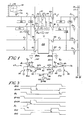
- Fig. 1 illustrates an MOS memory having a sense amplifier arrangement of the invention,
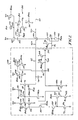
- Fig. 2 is a more detailed circuit diagram of a portion of Fig. 1, and
- Fig. 3 illustrates various waveforms which aid in describing the operation of the circuits of Figs. 1 and 2.
- Referring to Fig. 1, a representative portion of a dynamic MOS memory is shown which includes a preferred embodiment of a sense amplifier arrangement. The illustrated portion has four pairs of bit lines identified as A-B, C-D, E-F, and G-H. The pair of bit lines A-B is coupled through
isolation transistors isolation transistors 16 and 18. With this so-called "multiplexed folded bit line-shared sense amplifier" arrangement, the sense amplifier 14 is adapted by decoding circuitry to sense the potentials on bit lines A and B or on bit lines C and D. The pairs of bit lines E-F and G-H are similarly connected to anothersense amplifier 20. As described in further detail below, one of the bit lines for each pair (A, for example) is coupled to a capacitor associated with an addressed memory cell so that a charge transfer occurs between that bit line and the latter capacitor. The other bit line in that pair (B, for example) carries a reference voltage induced by a dummy cell capacitor. The sense amplifier detects the voltage difference between bit lines A and B and latches in a state representing this difference. The latched state of the sense amplifier therefore represents the logic level of the addressed memory cell. Thereafter, the decoding circuitry enables the data on the bit lines A and B to be coupled to input/output (I/O andTTO)buss lines 17 and 19 via bit lines C and D. The advantage of this arrangement is that the noise carried on bit line A is also carried on bit line B because the two bit lines are physically close to each other. Hence, there is good common mode noise rejection. - The above described arrangement is contrasted with the prior art wherein the sense amplifier detects the voltage difference between diagonally opposite bit lines A and D or B and C. For example, to sense the bit lines A and D,
transistors I/O buss 19 via a transistor DT, the state of the sense amplifier is readily ascertained. Hence, bit line D provides a path for sensing the state of the amplifier 14. Bit lines B and C are used in the same manner. - Although the conventional sense amplifier arrangement provides a convenient path for coupling the sense amplifier to the I/O and 170 busses, it is undesirably sensitive to noise. Bit lines A and B are usually physically close to each other, as are bit lines C and D. However, bit lines A and D (and B and C) are physically separated from each other on the memory chip. Hence, any noise which affects bit line A will probably not influence bit line D in the same manner. The conventional sense amplifier arrangement senses bit lines having different amounts of noise and is therefore, susceptible to developing noise- induced errors. Because the present arrangement senses bit lines which are physically near each other on the chip, noise problems are reduced. In addition, switch circuitry described below permits the state of the sense amplifiers to be conveniently transferred to the t/0 and
I/O busses. - Referring more specifically to the sense amplifier 14, this device includes
transistors voltage nodes transistor 10 is coupled to the drain of thetransistor 22 and to the gate of thetransistor 24. Terminal 12a of thetransistor 12 is coupled to the drain of thetransistor 24 and to the gate of thetransistor 22. The sense amplifier is coupled to a latching transistor 25 whose gate is driven by clock signal 0̸SD. - The bit lines C and D are coupled via
transistors 16 and 18, respectively, to the sense amplifier 14. As shown, terminal 16a of the transistor 16 is coupled to the drain oftransistor 22 and to the gate oftransistor 24. In addition, terminal 18a of thetransistor 18 is coupled to the drain of thetransistor 24 and to the gate of thetransistor 22. From the above described arrangement, either thetransistor pair transistor pair 16 and 18 may be turned on to couple the sense amplifier 14 to bit lines A and B or to bit lines C and D. - An exemplary memory cell M1 is shown coupled to bit line A for accessing. Memory cell M1 includes a
transistor 26 and a memory cell capacitor Cm. This capacitor conventionally stores a charge which is indicative of the logic state of the cell M1. Aword line 28 is driven to a high level when the cell M1 is addressed so as to turn on thetransistor 26 and thereby couple the capacitor Cm to the bit line A.Additional memory cells 30, each similar to the cell M1, are also associated with bit line A and may be coupled thereto when addressed by their own word lines. Similarly, memory cells groups 32, 34, and 36 are associated with bit lines B, C, and D, respectively, and may be selectively coupled to their associated bit lines when addressed by their own word lines. - Referring to bit lines E and F, they are associated with memory cell groups (not shown) and are coupled to the
sense amplifier 20 viatransistors sense amplifier 20 viatransistors 42 and 44, respectively. Each memory cell group contains cells which are similar to the memory cell M1 and are addressed in a similar manner. Thesense amplifier 20 operates in the same manner as the sense amplifier 14 to sense the voltage differential between bit lines E and F or between bit lines G and H, depending on whethertransistors transistors 42 and 44 are energized. - When the memory cell M1 is addressed, its memory capacitor CM is coupled to the bit line A via the
transistor 26. Thus, a transfer of charge occurs between the latter capacitor and the bit line A, thereby altering the voltage level on that bit line. The voltage on bit line B is altered by a dummy cell D1 which is coupled to the bit line B and to another bit line (F, for example). Included in the dummy cell D1 is a dummy cell capacitor CD, preferably of the same size as the memory cell capacitor CM, and precharged to a reference voltage level (for example, 0 volts). In response to a signal on a dummy word line (not shown), the dummy capacitor is coupled to bit lines B and F such that substantially equal transfers of charge occur between the capacitor Co and the bit lines to which it is coupled. Thus, the charge on the dummy capacitor is split between both bit lines to alter the bit line voltages. Then the voltage on the bit line A is compared by the sense amplifier 14 with the voltage on the bit line B to determine the logic state of the memory cell M1. - A dummy cell D2, similarto the dummy cell D1, is coupled between the bit lines A and E. Likewise, similar dummy cells D3 and D4 are coupled between bit lines D-H and C-G, respectively. The dummy cells D2-D4 operate in a manner similar to the dummy cell D1 so as to alter the voltage on the bit lines to which they are coupled.
- It should be pointed out that the construction of the memory cells and the dummy cells is not part of the present inventon. Both types of cells may be conventional, although it is preferred that the dummy cells be constructed as described in US-A-4 363 111.
- Bit lines C; D, G and H are coupled via transistors Cn DT, GTI and HT, respectively, to the I/O or the
I/O buss lines. In the manner described below, the voltages on the selected pair of bit lines (for example, A and B) are sensed by the sense amplifiers and transferred to the buss lines via these transistors (for example, CT and DT). - In order to select a pair of bit lines, a clock signal, indicated as 0̸DPL, is generated and coupled via
line 60 to the gates of thetransistors line 62 to the gates of thetransistors sense amplifiers 14 and 20, respectively, the clock signal 0̸RPR is pulled low and the clock signal ØRPL is left floating above Vcc. Consequently,transistors transistors sense amplifier 20. Concurrently,transistors sense amplifiers 14 and 20. A more detailed description of the sensing operation is discussed below. - The clock signal 0̸RPL on
line 60 is generated by acircuit 64 which includes transistors 66-68 andcapacitor 70 which are coupled together atnode 72. The gate oftransistor 68 is driven by clock signal 0L whilecapacitor 70 couples clock signal 0̸SD tonode 72. Aswitch 74 is adapted to be closed for selectively couplingnode 72 to ground. - In a similar fashion, the clock signal 0̸RPR on
line 62 is generated by acircuit 76 which includes transistors 78-80 andcapacitor 82 which are all coupled to anode 84. The gate oftransistor 80 is driven by the clock signal 0L whilecapacitor 82 couples the clock signal ØSD tonode 84. Also, aswitch 86 is included for selectively couplingnode 84 to ground. -
Circuits lines switch 90. In addition, lines 60b and62b couple circuits switches Line 96 connectsswitches node 98 which is coupled via acapacitor 100 to a signal ORPK online 102. - To sense the bit lines A and B, the following operation occurs. Referring to Fig. 3, various waveforms of different clock inputs into the illustrated embodiment are shown with respect to time for a better understanding of the operation. Assuming that
lines switches switches line 96 is precharged to 5 volts. Therefore, there is no voltage across thecapacitor 100. The signal ORPK goes to 0 volts at time t1 (Figure 3) when theswitches lines line 62 down toward 0 volts from its precharged level of 9 volts. - Referring to
circuits nodes switch 74couples node 72 to ground and, accordingly, holdstransistor 66 off. Hence, the high level voltage online 60 is undisturbed. Sinceswitch 86 remains open, thenode 84 stays at the 5 volt level andtransistor 78 turns on to clamp the voltage online 62 to 5 volts minus 1 volt (the threshold voltage in this embodiment) or 4 volts. Consequently,transistors 16 and 18 are turned off while the 9 volt level online 60 keeps thetransistors - The bit lines have also been precharged to 5 volts. However, when the memory cells are coupled to the bit lines A and B, the voltage on bit line A may drop down to 4.8 volts and the voltage on bit line B may drop down to 4.9 volts. Next, the
sense amplifiers 14 and 20 are enabled by the signal ØSD going high to 5 volts at time t2. As a result, the latch transistor 25 turns on and enables the sense amplifier 14 to latch the voltage onnode 21 to 0 volts and to leave the voltage onnode 23 at about 4 volts. Because the 4 volts online 62 is being applied to the gates oftransistors 16 and 18, the 5 volts onnode 23 does not disturb the 5 volt precharge level on bit line D. Accordingly, the 5 volt potential on line D continues to be coupled toI/O buss line 19. On the other hand, the 0 volt level- onnode 21 turns on transistor 16 which then couples that 0 volt level to I/O buss line 17 via bit line C. - The 5 volt kick of signal ØSD is also coupled by
capacitors nodes Node 72 is not affected because it is still coupled to ground viaclosed switch 74. However, the voltage onnode 84 is driven upwardly to approximately 7 volts. As a result,transistor 78 turns on harder to pull the voltage online 62 up to 5 volts. This acts to improve the reading speed of the sense amplifiers by turning transistor 16 on harder, thereby enabling the 0 volts onnode 21 to be more easily coupled to the I/O buss line 17. Furthermore, the signal ØRPR online 62 is continuously held at approximately 5 volts whentransistor 78 is turned on hard. This is important in that if the signal ØRPR is not actively held at the 5 volt level, then a low level signal on either bit line C or D would be capacitively coupled toline 62 via the gate-source capacitance of eithertransistor 16 or 18. - After the voltage difference between bit lines A and B is read on the I/O and the
I/O buss lines 17 and 19, the memory cell is refreshed in the following manner. Theswitch 86 incircuitry 76 closes to groundnode 84 and turn thetransistor 78 off. Consequently, the signal ORPR online 62 is released from its clamped 5 volt level. Then the signal ORPK online 102 goes high at time t3. Simultaneously, theswitch 90 is closed to short the signal ØRPL online 60 to the signal ØRPR online 62. When thesense amplifiers 14 and 20 had previously sensed the voltage differentials, the signal ØRPL online 60 was pulled from 9 volts down to about 7 volts as a result of being capacitively coupled by thetransistors switch 90 and the signal ØRPK goes high, the signals ØRPL and ØRPL are first driven towards 6 volts and are then boosted back up to 7 volts to turn on all the isolation transistors. As a result, the sense amplifier couples bit line A to bit line C and bit line B to bit line D. - If a logic 1 were present in the memory cell capacitor Cm, the voltage on bit line A would have dropped to 4 volts as a result of the sense amplifier 14 sensing a logic 1 in the accessed cell M1 coupled to bit line A. However, the voltage on bit line C remains at 5 volts because
transistor 18 stays off. Therefore, when bit lines A and C are coupled by the sense amplifier 14, the bit line capacitance of bit lines A and C is shared and the voltage on both bit lines goes to 4.5 volts. Correspondingly, theword line 28 is held at high voltage (by circuitry not shown) so that the 4.5 volts on bit line A refreshes the accessed memory cell capacitor Cm. After the voltage on the word line goes low, theswitches - Fig. 2 illustrates a more
detailed circuit 104 for regulating the signal ØRPR' online 62. A duplicate circuit (not shown) controls the signal ØRPL online 60. Also, a more detailed circuit 106 of the elements common to the signals ØRPR and ØRPL is shown. Theswitch 94 in Fig. 1 is depicted in the form of transistor 94a in Fig. 2 and controlled by the circuitry arranged fromtransistors switch 86 in Fig. 1 is arranged fromtransistors 86a and 86b and their associated circuitry in Fig. 2. - Referring more specifically to the circuitry which controls transistor 94a,
transistors 108 and 110 are arranged as a push-pull driver for producing alternating high and low signals atnode 128. Clock signals ØPRS and ØXI are applied as inputs into the respective gates oftransistors 108 and 110. The signal onnode 128 is applied to the gate oftransistor 112 which is coupled totransistor 114 so as to form another push-pull driver for producing alternating high and low signals atnode 130. The clock signals ØAOR and ØPRS are applied as inputs into terminal 112a oftransistor 112 and the gate oftransistor 114, respectively. - The signal on
node 130 is coupled by capacitor 16 tonode 132 which is, in turn, coupled vialine 134 to the gate of transistor 94a. A pair of transistors 136 and 138 are also coupled toline 134 betweennode 132 and the gate of transistor 94a with clock signals ØPRS and ØL being applied as inputs to the gates of transistors 136 and 138. To complete the control circuitry for transistor 94a, a pair of push-pull drivers are arranged fromtransistors transistors transistor 118 which is coupled tonode 132. Clock signal ØPRS and the signal from row address A7 are applied to the. gates of push-pull transistors transistor 120. The signal from A7 is applied to the gate oftransistor 122 while the clock signal ØAOR is applied to the source oftransistor 120. The push-pull transistors node 142. The signal onnode 142 is then applied vianode 144 to the gate oftransistor 118, and the terminal 118a of the same transistor is coupled tonode 132. - The transistor 94a is turned on by the above-mentioned control circuitry in the following manner. During precharging, the signal ØPRS is at a high level. Consequently,
transistors nodes transistor 114 turns on to hold the signal onnode 130 at ground. When A7 reaches the logic 1 state at time t4 (See Figure 3)transistor 126 turns on. As a result, the signal onnode 140 is pulled to ground. Concurrently, A7 turns ontransistor 122 which, in turn, holds the signal onnode 142 to ground. When the signal OAOR goes high at time ts, the signal onnode 142 remains low because thetransistor 120 is still off due to the signal onnode 140 also being low. However, the signal onnode 130 goes high becausetransistor 112 is turned on. The positive transition onnode 130 is coupled throughcapacitor 116 tonode 132, thereby pulling up the signal onnode 132. The high signal onnode 132 is coupled vialine 134 to the gate of transistor 94a, thereby turning on transistor 94a. - More detailed circuitry for the
switch 74 of Fig. 1 is not shown in Fig. 2. However, the circuitry forswitch 74 is the duplicate circuitry of that disclosed forswitch 86. In Fig: 2, switch 86 is depicted bytransistors 86a and 86b and associated circuitry. The gate oftransistor 86b is coupled tonode 144 while the terminal 86bb oftransistor 86b is coupled tonode 146. The transistor 86a is arranged such that its gate is coupled to a pair of push-pull transistors 148 and 150. The gate of transistor 148 is driven by a clock signal ØKI, while the gate of transistor 150 is driven by the clock signal OPRS. The transistor 148 is coupled to the transistor 150 atnode 152 which, in turn, is connected to the gate of transistor 86a. The transistor 86a is coupled vianode 154 to thetransistor 156.Node 154 is also coupled tonode 146. The gate oftransistor 156 is driven by the clock signal ØPRS. - Just as in Fig. 1,
transistor 80 is coupled totransistor 82 atnode 84, and. the gate oftransistor 80 is driven by the clock signal 0L. Also, 84 is coupled totransistor 78 which is connectedto.line 62. However,capacitor 158 has been added to couple the signal 0L on the gate oftransistor 80 to thenode 146. In addition,, acapacitor 79 is coupled totransistor 78 online 62. - As mentioned above, transistors representing the
switch 74 are not shown in Fig. 2 althoughtransistors 86a and 86b and their peripheral circuitry duplicate that ofswitch 74. Therefore, for purposes of explanation, assume that the transistors forswitch 74 aretransistors 86a and 86b. Also, assume that the inputs to the gates oftransistors A 7 rather than A7 such that A7 is at a logic 0 state. When the signal OAOR rises at time t5, the signal onnode 142 andnode 144 is pulled high bytransistor 120 to turntransistor 86b on. As a result, the signal onnode 84 is pulled to ground. Then the clock signal ØSD rises at time t2. This rise is coupled viacapacitor 82 tonode 84. However,node 84 remains low becausetransistor 86b is on. For signal ØRPR online 62,transistor 86b is turned off. Hence,node 84 is capacitively coupled to about 7 volts as the clock signal 0so rises at time t2. As a result, the signal ØRPR is clamped to 5 volts during sense amplifier latching. - The
switch 86 is closed when the signal ØKI rises at time t6 (See Figure 3) to turn on transistor 148, thereby pulling the signal onnode 152 high to turn on transistor 86a. As a result, the signal onnode 84 is pulled to ground. It should be noted that the signal onnode 152 had previously been precharged low by the clock signal OPRS via transistor 150. -
Switch 90 in Fig. 1 is depicted bytransistor 90a and its associated circuitry in Fig. 2. The drain and source oftransistor 90a are connected tolines transistor 90a andnode 162 are capacitively coupled bytransistor 160 to the clock signal ORPK online 102. This signal is also coupled bycapacitor 100 tonode 98 which, in turn, is connected online 96 to the transistor 94a and to transistor 99 being driven by the clock signal ØL. -
Node 162 is coupled to push-pull transistors transistor 166 is coupled to clock signal 0x, while the gate of the same transistor is driven by signal ØAOR. The gate oftransistor 162 is driven by the signal on node 168 which is coupled totransistors Transistor 170 capacitively couples node 168 to signal 0sp. The gate oftransistor 172 is driven by the signal OPRS, while the gate oftransistor 174 is driven by the signal onnode 176. This signal, in turn, is developed by push-pull transistors node 176. The gate oftransistor 178 is driven by signal ØKI. while the gate oftransistor 180 is driven by signal OPRS. - To turn on
transistor 90a, the signal on node 168 is precharged to 4 volts by the signal ØPRS turning ontransistor 172. Thereafter, the signal ØSD goes high at time t2, and this high is capacitively coupled bytransistor 170 to node 168. As a result, the signal on node 168 is kicked up to 7 volts. Accordingly,transistor 164 is pulled on to pull the signal onnode 162 to the 5 volt level. When the signal ORPK goes high at time t3, the high is capacitively coupled bycapacitor 160 to kick up the signal on the gate oftransistor 90a. Hence,transistor 90a turns on toshort lines transistor 164 turned off while the signal on the gate oftransistor 90a is kicked up to avoid losing charge to Vcc viatransistor 164. In order to do this, the signal ØKI turns ontransistor 178 to raise the signal onnode 176, and, consequently, thetransistor 174 turns on to pull down the signal on node 168. - The low to high transition of the signal ORPK is also capacitively coupled via
transistor 100 andnode 98 to transistor 94a for driving the signal on shortedlines lines
Claims (12)
Applications Claiming Priority (2)
| Application Number | Priority Date | Filing Date | Title |
|---|---|---|---|
| US06/195,728 US4351034A (en) | 1980-10-10 | 1980-10-10 | Folded bit line-shared sense amplifiers |
| US195728 | 1994-02-14 |
Publications (3)
| Publication Number | Publication Date |
|---|---|
| EP0049990A2 EP0049990A2 (en) | 1982-04-21 |
| EP0049990A3 EP0049990A3 (en) | 1982-10-13 |
| EP0049990B1 true EP0049990B1 (en) | 1987-05-27 |
Family
ID=22722538
Family Applications (1)
| Application Number | Title | Priority Date | Filing Date |
|---|---|---|---|
| EP81304614A Expired EP0049990B1 (en) | 1980-10-10 | 1981-10-05 | Folded bit line-shared sense amplifiers |
Country Status (5)
| Country | Link |
|---|---|
| US (1) | US4351034A (en) |
| EP (1) | EP0049990B1 (en) |
| JP (1) | JPS5792486A (en) |
| CA (1) | CA1175939A (en) |
| DE (1) | DE3176224D1 (en) |
Families Citing this family (27)
| Publication number | Priority date | Publication date | Assignee | Title |
|---|---|---|---|---|
| JPS5745267A (en) * | 1980-09-01 | 1982-03-15 | Nec Corp | Semiconductor device |
| US4413329A (en) * | 1980-12-24 | 1983-11-01 | International Business Machines Corporation | Dynamic memory cell |
| US4739497A (en) * | 1981-05-29 | 1988-04-19 | Hitachi, Ltd. | Semiconductor memory |
| US4442508A (en) * | 1981-08-05 | 1984-04-10 | General Instrument Corporation | Storage cells for use in two conductor data column storage logic arrays |
| US4402063A (en) * | 1981-09-28 | 1983-08-30 | Bell Telephone Laboratories, Incorporated | Flip-flop detector array for minimum geometry semiconductor memory apparatus |
| US4494220A (en) * | 1982-11-24 | 1985-01-15 | At&T Bell Laboratories | Folded bit line memory with one decoder per pair of spare rows |
| USRE33266E (en) * | 1982-11-24 | 1990-07-17 | American Telephone And Telegraph Company, At&T Bell Laboratories | Folded bit line memory with one decoder per pair of spare rows |
| US4584672A (en) * | 1984-02-22 | 1986-04-22 | Intel Corporation | CMOS dynamic random-access memory with active cycle one half power supply potential bit line precharge |
| US4961166A (en) * | 1984-05-07 | 1990-10-02 | Hitachi, Ltd. | Dynamic RAM having a full size dummy cell |
| JPS6150284A (en) * | 1984-08-17 | 1986-03-12 | Mitsubishi Electric Corp | Driving method of shared sense amplifier circuit |
| JPS6150283A (en) * | 1984-08-17 | 1986-03-12 | Mitsubishi Electric Corp | Drive circuit of shared sense amplifier circuit |
| JPH0793009B2 (en) * | 1984-12-13 | 1995-10-09 | 株式会社東芝 | Semiconductor memory device |
| DE3680843D1 (en) * | 1985-08-30 | 1991-09-19 | Sgs Thomson Microelectronics | PARALLEL LINE PER LINE DATA TRANSFER IN RAM. |
| JPS6280897A (en) * | 1985-10-04 | 1987-04-14 | Mitsubishi Electric Corp | semiconductor storage device |
| US4807195A (en) * | 1987-05-18 | 1989-02-21 | International Business Machines Corporation | Apparatus and method for providing a dual sense amplifier with divided bit line isolation |
| JPH01184787A (en) * | 1988-01-19 | 1989-07-24 | Toshiba Corp | Semiconductor memory |
| DE3937068C2 (en) * | 1988-11-07 | 1994-10-06 | Toshiba Kawasaki Kk | Dynamic semiconductor memory device |
| JPH02201797A (en) * | 1989-01-31 | 1990-08-09 | Toshiba Corp | Semiconductor memory device |
| JP2742719B2 (en) * | 1990-02-16 | 1998-04-22 | 三菱電機株式会社 | Semiconductor storage device |
| US5046050A (en) * | 1990-04-10 | 1991-09-03 | National Semiconductor Corporation | Shared BiCMOS sense amplifier |
| US5241503A (en) * | 1991-02-25 | 1993-08-31 | Motorola, Inc. | Dynamic random access memory with improved page-mode performance and method therefor having isolator between memory cells and sense amplifiers |
| JPH06195973A (en) * | 1992-10-12 | 1994-07-15 | Nec Corp | Dynamic RAM |
| US5572459A (en) * | 1994-09-16 | 1996-11-05 | Ramtron International Corporation | Voltage reference for a ferroelectric 1T/1C based memory |
| US5836007A (en) * | 1995-09-14 | 1998-11-10 | International Business Machines Corporation | Methods and systems for improving memory component size and access speed including splitting bit lines and alternate pre-charge/access cycles |
| US5636170A (en) * | 1995-11-13 | 1997-06-03 | Micron Technology, Inc. | Low voltage dynamic memory |
| US5999459A (en) * | 1998-05-27 | 1999-12-07 | Winbond Electronics Corporation | High-performance pass-gate isolation circuitry |
| JP2007095264A (en) * | 2005-09-29 | 2007-04-12 | Hynix Semiconductor Inc | Semiconductor memory device having shared bit line sense amplifier scheme and driving method thereof |
Citations (1)
| Publication number | Priority date | Publication date | Assignee | Title |
|---|---|---|---|---|
| DE2647394B1 (en) * | 1976-10-20 | 1978-03-16 | Siemens Ag | MOS semiconductor memory device |
Family Cites Families (4)
| Publication number | Priority date | Publication date | Assignee | Title |
|---|---|---|---|---|
| US3560940A (en) * | 1968-07-15 | 1971-02-02 | Ibm | Time shared interconnection apparatus |
| JPS54148340A (en) * | 1978-05-12 | 1979-11-20 | Nec Corp | Memory circuit |
| DE2919166C2 (en) * | 1978-05-12 | 1986-01-02 | Nippon Electric Co., Ltd., Tokio/Tokyo | Storage device |
| US4279023A (en) * | 1979-12-19 | 1981-07-14 | International Business Machines Corporation | Sense latch |
-
1980
- 1980-10-10 US US06/195,728 patent/US4351034A/en not_active Ceased
-
1981
- 1981-03-17 CA CA000373225A patent/CA1175939A/en not_active Expired
- 1981-10-05 JP JP56158569A patent/JPS5792486A/en active Granted
- 1981-10-05 DE DE8181304614T patent/DE3176224D1/en not_active Expired
- 1981-10-05 EP EP81304614A patent/EP0049990B1/en not_active Expired
Patent Citations (1)
| Publication number | Priority date | Publication date | Assignee | Title |
|---|---|---|---|---|
| DE2647394B1 (en) * | 1976-10-20 | 1978-03-16 | Siemens Ag | MOS semiconductor memory device |
Also Published As
| Publication number | Publication date |
|---|---|
| DE3176224D1 (en) | 1987-07-02 |
| US4351034A (en) | 1982-09-21 |
| CA1175939A (en) | 1984-10-09 |
| JPH0115957B2 (en) | 1989-03-22 |
| EP0049990A2 (en) | 1982-04-21 |
| EP0049990A3 (en) | 1982-10-13 |
| JPS5792486A (en) | 1982-06-09 |
Similar Documents
| Publication | Publication Date | Title |
|---|---|---|
| US4351034A (en) | Folded bit line-shared sense amplifiers | |
| US5241503A (en) | Dynamic random access memory with improved page-mode performance and method therefor having isolator between memory cells and sense amplifiers | |
| US4932002A (en) | Bit line latch sense amp | |
| US4062000A (en) | Current sense amp for static memory cell | |
| US4363111A (en) | Dummy cell arrangement for an MOS memory | |
| US20010037429A1 (en) | Balanced switching method and circuit | |
| US5185722A (en) | Semiconductor memory device having a memory test circuit | |
| US6438049B1 (en) | Variable equilibrate voltage circuit for paired digit lines | |
| US4397003A (en) | Dynamic random access memory | |
| JPH07226087A (en) | Semiconductor memory device | |
| US4112512A (en) | Semiconductor memory read/write access circuit and method | |
| JPH05166365A (en) | Dynamic semiconductor memory device | |
| US4622655A (en) | Semiconductor memory | |
| US4338679A (en) | Row driver circuit for semiconductor memory | |
| US4451906A (en) | Dynamic type memory device having improved operation speed | |
| JPH06162776A (en) | Semiconductor memory circuit | |
| JPS649680B2 (en) | ||
| EP0541240B1 (en) | High speed testing of field-effect transistors | |
| US5771187A (en) | Multiple level storage DRAM cell | |
| US5796666A (en) | Method and apparatus for quickly restoring digit I/O lines | |
| USRE32682E (en) | Folded bit line-shared sense amplifiers | |
| US5428564A (en) | Six transistor dynamic content addressable memory circuit | |
| US5515315A (en) | Dynamic random access memory | |
| US5894434A (en) | MOS static memory array | |
| US6301178B1 (en) | Reduced cell voltage for memory device |
Legal Events
| Date | Code | Title | Description |
|---|---|---|---|
| PUAI | Public reference made under article 153(3) epc to a published international application that has entered the european phase |
Free format text: ORIGINAL CODE: 0009012 |
|
| AK | Designated contracting states |
Designated state(s): DE FR GB NL |
|
| PUAL | Search report despatched |
Free format text: ORIGINAL CODE: 0009013 |
|
| AK | Designated contracting states |
Designated state(s): DE FR GB NL |
|
| 17P | Request for examination filed |
Effective date: 19830406 |
|
| 17Q | First examination report despatched |
Effective date: 19851009 |
|
| RAP1 | Party data changed (applicant data changed or rights of an application transferred) |
Owner name: INMOS CORPORATION |
|
| GRAA | (expected) grant |
Free format text: ORIGINAL CODE: 0009210 |
|
| AK | Designated contracting states |
Kind code of ref document: B1 Designated state(s): DE FR GB NL |
|
| REF | Corresponds to: |
Ref document number: 3176224 Country of ref document: DE Date of ref document: 19870702 |
|
| ET | Fr: translation filed | ||
| PLBE | No opposition filed within time limit |
Free format text: ORIGINAL CODE: 0009261 |
|
| STAA | Information on the status of an ep patent application or granted ep patent |
Free format text: STATUS: NO OPPOSITION FILED WITHIN TIME LIMIT |
|
| 26N | No opposition filed | ||
| PGFP | Annual fee paid to national office [announced via postgrant information from national office to epo] |
Ref country code: FR Payment date: 20000918 Year of fee payment: 20 |
|
| PGFP | Annual fee paid to national office [announced via postgrant information from national office to epo] |
Ref country code: GB Payment date: 20000921 Year of fee payment: 20 |
|
| PGFP | Annual fee paid to national office [announced via postgrant information from national office to epo] |
Ref country code: NL Payment date: 20000925 Year of fee payment: 20 |
|
| PGFP | Annual fee paid to national office [announced via postgrant information from national office to epo] |
Ref country code: DE Payment date: 20001229 Year of fee payment: 20 |
|
| PG25 | Lapsed in a contracting state [announced via postgrant information from national office to epo] |
Ref country code: GB Free format text: LAPSE BECAUSE OF EXPIRATION OF PROTECTION Effective date: 20011004 |
|
| PG25 | Lapsed in a contracting state [announced via postgrant information from national office to epo] |
Ref country code: NL Free format text: LAPSE BECAUSE OF EXPIRATION OF PROTECTION Effective date: 20011005 |
|
| REG | Reference to a national code |
Ref country code: GB Ref legal event code: PE20 Effective date: 20011004 |
|
| NLV7 | Nl: ceased due to reaching the maximum lifetime of a patent |
Effective date: 20011005 |