EP0049988B1 - High speed data transfer for a semiconductor memory - Google Patents
High speed data transfer for a semiconductor memory Download PDFInfo
- Publication number
- EP0049988B1 EP0049988B1 EP81304605A EP81304605A EP0049988B1 EP 0049988 B1 EP0049988 B1 EP 0049988B1 EP 81304605 A EP81304605 A EP 81304605A EP 81304605 A EP81304605 A EP 81304605A EP 0049988 B1 EP0049988 B1 EP 0049988B1
- Authority
- EP
- European Patent Office
- Prior art keywords
- decoder
- data
- output
- input
- node
- Prior art date
- Legal status (The legal status is an assumption and is not a legal conclusion. Google has not performed a legal analysis and makes no representation as to the accuracy of the status listed.)
- Expired
Links
- 239000004065 semiconductor Substances 0.000 title claims description 8
- 230000015654 memory Effects 0.000 claims description 60
- 239000000872 buffer Substances 0.000 claims description 45
- 230000004044 response Effects 0.000 claims description 23
- 230000008878 coupling Effects 0.000 claims description 4
- 238000010168 coupling process Methods 0.000 claims description 4
- 238000005859 coupling reaction Methods 0.000 claims description 4
- 230000002401 inhibitory effect Effects 0.000 claims description 3
- 238000009877 rendering Methods 0.000 claims 1
- 238000010276 construction Methods 0.000 description 4
- 230000000295 complement effect Effects 0.000 description 3
- 238000010586 diagram Methods 0.000 description 3
- 230000004075 alteration Effects 0.000 description 2
- 230000008901 benefit Effects 0.000 description 2
- 230000000694 effects Effects 0.000 description 2
- 230000006870 function Effects 0.000 description 2
- 238000000034 method Methods 0.000 description 2
- 230000004048 modification Effects 0.000 description 2
- 238000012986 modification Methods 0.000 description 2
- 230000008569 process Effects 0.000 description 2
- 230000004913 activation Effects 0.000 description 1
- 239000003990 capacitor Substances 0.000 description 1
- 230000008859 change Effects 0.000 description 1
- WABPQHHGFIMREM-FTXFMUIASA-N lead-202 Chemical compound [202Pb] WABPQHHGFIMREM-FTXFMUIASA-N 0.000 description 1
Images


Classifications
-
- G—PHYSICS
- G11—INFORMATION STORAGE
- G11C—STATIC STORES
- G11C8/00—Arrangements for selecting an address in a digital store
- G11C8/10—Decoders
-
- G—PHYSICS
- G11—INFORMATION STORAGE
- G11C—STATIC STORES
- G11C7/00—Arrangements for writing information into, or reading information out from, a digital store
- G11C7/10—Input/output [I/O] data interface arrangements, e.g. I/O data control circuits, I/O data buffers
- G11C7/1015—Read-write modes for single port memories, i.e. having either a random port or a serial port
- G11C7/103—Read-write modes for single port memories, i.e. having either a random port or a serial port using serially addressed read-write data registers
- G11C7/1033—Read-write modes for single port memories, i.e. having either a random port or a serial port using serially addressed read-write data registers using data registers of which only one stage is addressed for sequentially outputting data from a predetermined number of stages, e.g. nibble read-write mode
-
- G—PHYSICS
- G11—INFORMATION STORAGE
- G11C—STATIC STORES
- G11C7/00—Arrangements for writing information into, or reading information out from, a digital store
- G11C7/10—Input/output [I/O] data interface arrangements, e.g. I/O data control circuits, I/O data buffers
- G11C7/1015—Read-write modes for single port memories, i.e. having either a random port or a serial port
- G11C7/1045—Read-write mode select circuits
-
- G—PHYSICS
- G11—INFORMATION STORAGE
- G11C—STATIC STORES
- G11C7/00—Arrangements for writing information into, or reading information out from, a digital store
- G11C7/10—Input/output [I/O] data interface arrangements, e.g. I/O data control circuits, I/O data buffers
- G11C7/1051—Data output circuits, e.g. read-out amplifiers, data output buffers, data output registers, data output level conversion circuits
- G11C7/106—Data output latches
-
- G—PHYSICS
- G11—INFORMATION STORAGE
- G11C—STATIC STORES
- G11C7/00—Arrangements for writing information into, or reading information out from, a digital store
- G11C7/10—Input/output [I/O] data interface arrangements, e.g. I/O data control circuits, I/O data buffers
- G11C7/1051—Data output circuits, e.g. read-out amplifiers, data output buffers, data output registers, data output level conversion circuits
- G11C7/1066—Output synchronization
-
- G—PHYSICS
- G11—INFORMATION STORAGE
- G11C—STATIC STORES
- G11C8/00—Arrangements for selecting an address in a digital store
- G11C8/04—Arrangements for selecting an address in a digital store using a sequential addressing device, e.g. shift register, counter
-
- G—PHYSICS
- G11—INFORMATION STORAGE
- G11C—STATIC STORES
- G11C8/00—Arrangements for selecting an address in a digital store
- G11C8/18—Address timing or clocking circuits; Address control signal generation or management, e.g. for row address strobe [RAS] or column address strobe [CAS] signals
Definitions
- the present invention relates to a system for rapidly transferring data to and from a plurality of successive memory locations of a semiconductor memory.
- page mode operation for rapidly reading the data stored in successive memory locations.
- the data in one row of the memory is latched in a plurality of sense amplifiers.
- successive column addresses are input to the memory to successively output the data stored in each sense amplifier.
- successive row addresses are not required to read the data in each successive location in the accessed row, a two-to-one time saving is achieved in reading data.
- the ratio of a standard read-write cycle time to page mode cycle time (typically a factor of two) is frequently not large enough to warrant the added system complexity required to implement page mode operation.
- EP-A-45063 which is a conflicting European application in accordance with Article 54(3) EPC, shows a rapid data transfer system of the type described above in which the shift register and column decoder functions are integrated.
- a system for rapidly transferring data to and from a plurality of successive memory locations of a semiconductor memory comprising
- An embodiment of the invention has the advantage that the system transfers data more rapidly and with less complexity than conventional page mode systems.
- the present invention causes data stored in successive locations in a semiconductor memory to be rapidly read out of memory in response to a single address input.
- the system includes a plurality of N data latches for storing data associated with N successive memory locations. The latter locations are defined by a plurality of bits of the address input.
- each decoder being associated with one data latch.
- one decoder is enabled for causing its associated data latch to output its stored data.
- the latter decoder then disabled itself and enables the next decoder so that a second latch outputs its stored data.
- the process continues with each decoder disabling itself and enabling the next decoder so that the data latches are caused to sequentially output their stored data.
- rapid writing of data into memory is effected by including N data buffers.
- the buffers receive incoming data and are adapted to output that data to N successive memory locations when the memory is in its write mode.
- Each buffer is controlled by one of the decoders which are sequentially enabled as described above. When enabled, a decoder causes its associated buffer to output its data to memory.
- the N buffers are sequentially selected to cause the incoming data to be written into N successive memory locations.
- Fig. 1 there is shown a system for rapidly reading data from and writing data into successive locations in a semiconductor memory.
- "nibble mode" operation is effected whereby four bits of data are read from or written into four successive memory locations in response to a single address input.
- the system includes four data latches, shown as output sense amplifiers A0, A1, A2, and A3, and four decoders D0, D1, D2, and D3, each of the latter being associated with one of the sense amplifiers.
- the sense amplifiers store four bits of data, one bit per sense amplifier, received from four successive memory locations which are identified by six bits of an eight bit address input.
- each of the decoders is adapted to be enabled for causing its associated sense amplifier to output stored data to a data buss 10 via an output latch 12.
- each decoder receives two bits of the address input such that one of the decoders, DO for example, is enabled in response to the selected two address bits having a given logic state for causing the sense amplifier AO to output a bit of stored data. Then the enabled decoder disables itself and enables a successive decoder, D1 for example, so that its sense amplifier A1 outputs its stored data. The cycle continues with each decoder disabling itself and enabling the next decoder so that the sense amplifiers are enabled in succession. Thus, four bits of data are output to the data buss 10 in response to a single address input.
- the decoders DO-D3 are also adapted to be successively enabled for causing four associated data input buffers, BO ⁇ B3, to successively apply four bits of input data to four successive locations in memory in response to a single address input.
- the illustrated system operates in the "nibble mode" to effect rapid writing of data into memory and rapid reading of data out of memory.
- the output sense amplifier AO is adapted to store a data bit and its complement received from a memory location via data busses identified as DBo and DBo.
- the amplifier A1 is adapted to store a data bit and its complement received from a successive memory location via data busses OB 1 and DB 1.
- the amplifiers A2 and A3 are likewise adapted to store data bits and their complements received via busses DB 2 , DB 2 , and DB 3 , DB 3 , respectively.
- the data bits carried by the busses DB 0 ⁇ DB 3 (and their complements) are received from four successive memory locations which are defined by six bits of an eight bit address input to the memory.
- the output of the amplifier AO is coupled to the drains of MOS transistors 14 and 16, and the sources of the latter transistors are coupled via leads 18 and 20 to the input of the output latch 12.
- the amplifiers Al-A3 are coupled to the output latch 12 by means of transistors 22, 24, 26, 28, 30, and 32.
- the decoder DO receives two selected bits, AO and A1, of the input address via leads 34 and 36.
- the remaining decoders D1 ⁇ D3 receive the same address bits, but in different logic combinations, so that only one decoder will be initially selected or enabled.
- the decoder D1 for example, receives AO and A1
- the decoder D2 receives AO and A1
- the decoder D3 receives AO and A1.
- the decoder DO is enabled. Consequently, the decoders D1 ⁇ D3 are all disabled.
- the decoder D1 is enabled and the other decoders are disabled. Suffice it to say that the decoders' input bits will have a given logic state which will enable any one of the decoders DO-D3. The enablement of the remaining decoders is described below.
- the decoders DO-D3 also preferably receive a clock signal identified as ⁇ POF. After a decoder has been selected, the signal ⁇ POF clocks its operation as described below.
- the decoder DO develops an output signal YO when the clock signal ( ⁇ POF goes low at time t 1 , as shown in Fig. 2.
- the signal YO is coupled via a lead 38 to the gates of transistors 14 and 16 for turning them on.
- the data stored in the amplifier AO is coupled via transistors 14 and 16 to the leads 18 and 20, to the output latch 12, and then to the output buss 10.
- the high or low level data output thus applied to the buss 10 is represented by DO in Fig. 2.
- the decoder DO then disables itself to turn off the transistors 14 and 16 and couples its output signal Y0 to the next successive decoder D1 via a lead 40.
- the decoder D1 is selected so that when the signal ⁇ POF goes low again at time t2 (Fig. 2), it develops an output signal Y1 on lead 42 for turning on transistors 22 and 24.
- output data D1 (Fig. 2) from the amplifier A1 is coupled to the output buss 10.
- the decoder D1 then disables itself to turn off the transistors 22 and 24 and couples its signal Y1 to the decoder D2 to select the latter for enablement.
- the process described above continues so that the decoders D2 and D3 are successively enabled for causing the output of data D2 and D3 (Fig. 2) in synchronism with the clock pulse ( ⁇ POF ⁇
- the decoder D3 selects the decoder DO via a signal Y3 on a lead 44. Hence, each of the decoders may be selected for another cycle of rapid data reading. Alternately, the nibble read cycle described above may be followed by a conventional read cycle as shown in Fig. 2.
- the nibble mode cycle may start with whatever decoder is first selected by a pair of low logic level input bits. Thereafter, the other decoders are successively selected 'until the four sense amplifiers Ao-A3 have output their stored data.
- each of the data input buffers is coupled to associated data busses and receives input data via a pair of transistors which are controlled by one of the decoders.
- the buffer BO receives an input data bit Din and its complement Din via transistors 46 and 48.
- the output of the buffer BO is coupled to the data busses DB o and DB O .
- the buffers B1-B3 are similarly connected to couple input data to their respective data busses.
- the decoder DO may be enabled as described previously for turning on the transistors 46 and 48 for coupling the input data to the busses DB o and DB o .
- the decoders D1 ⁇ D3 are then successively enabled as described above for reading three more bits of input data to the remaining busses. In this manner, four bits of input data may be rapidly written into four successive locations in memory.
- the output sense amplifiers AO-A3 and the output latch 12 may be conventional.
- the decoders DO-D3 are all the same, each being preferably constructed as shown in Fig. 3.
- the buffers BO-B3 are also of the same construction, one of which is shown in Fig. 4.
- Fig. 6 depicts waveforms of the various input signals, output signals and clock signals associated with the circuitry of Figs. 3 and 4.
- Fig. 5 is an index which relates the signals developed by the circuitry of Fig. 3 to the various decoders.
- the circuitry of Fig. 3 represents the decoder D0
- Y is the signal YO developed by the decoder D0
- Y i+3 is the signal Y3 developed by the decoder D3.
- the circuitry of Fig. 3 represents the decoder D1, Y ; represents the signal Y1 developed by the decoder D1
- Y i+3 represents the signal YO developed by the decoder Y0.
- the illustrated decoder receives its address inputs AO (or AO) and A1 (or A1 ) at the gates of transistors 50 and 52.
- An output lead 54 carries the output signal Y ; developed by the decoder. That output is employed to cause the decoder's associated sense amplifer to output its stored data, and it is also applied to the gates of transistors 56 and 58.
- the signal Y represents the signal YO shown in Fig. 1.
- a signal identified as Y, +3 is applied to the gate of a transistor 60.
- the signal Y, +3 is the signal Y3 shown in Fig. 1 and corresponds to the Y, output of the decoder D3.
- the illustrated decoder receives a precharge signal ⁇ D (see Fig. 6) which is initially high and which is applied to the gate of a transistor 62 for raising its source (node 64) to a high level.
- a clock signal ⁇ OD2 (Fig. 6) is also high and is applied to the gate of a transistor 66 which is coupled to the node 64.
- the drain of transistor 66 (node 68) is also driven high.
- the signal ⁇ D is also applied to the gate of a transistor 70 for precharging node 72 to a high level. Consequently, transistors 74 and 76 are turned on for pulling their drain connections (nodes 78 and 80) to a low level.
- the gate of another transistor 82 receives ⁇ D for raising the voltage at node 84 so as to turn on transistors 86 and 88 and pull their drain connections (nodes 90 and 92) to a low level.
- a transistor 94 which is coupled to the node 90 via its gate is thus turned off, as is a transistor 96 whose gate is coupled to node 92.
- the source of the transistor 96 is coupled via a node 98 to a transistor 100 whose gate receives the signal ⁇ D. Consequently, the latter transistor is turned on to lower the voltage at the node 98.
- a transistor 102 whose gate is also coupled to the node 98 is therefore turned off.
- the drain of the latter transistor is coupled to the node 64 but, since the latter transistor is now off, it does not disturb the high level to which the node 64 is precharged.
- the signal ⁇ POF (see Figs. 1 and 6) is high at this time and is applied to a transistor 104 whose gate is coupled to the node 78 and whose source is coupled to the node 80. Because the node 78 is at a low level, the transistor 104 is held off and the node 80 remains at a low level. The node 80 is also coupled to the gate of another transistor 106 which is also held off at this time.
- the signal ⁇ POF is also applied to the transistor 94. Because the gate of the transistor 94 is coupled to the low level on node 90, the transistor 94 remains off and the potential at its source (node 92) remains low.
- the node 64 remains at a high level as does the node 68.
- the latter node is coupled to the gate of a transistor 108 whose drain receives the signal ⁇ YO. Because ⁇ YO is high (see Fig. 6), the transistor 108 develops a high level output Y, at the lead 54.
- the lead 54 is also coupled to the drain of a transistor 109 whose gate lead 111 is coupled (via a connection which is not shown) to the node 80. It will be recalled that the node 80 was pulled low during the precharge cycle. Hence, the transistor 109 is held off to permit the signal Y, at lead 54 to go high.
- the illustrated decoder represents the decoder DO (Fig. 1)
- Yi represents YO and the transistors 14 and 16 (Fig. 1) are turned on. All the other decoders are off because at least one of their address inputs is high.
- At least one of the transistors which corresponds to transistors 50 and 52 in the other decoders is turned on for pulling low the voltage at nodes corresponding to nodes 64 and 68, thereby inhibiting ⁇ YO from driving Y, high in the other decoders.
- each of the decoders is adapted to disable itself after its associated sense amplifier has output its stored data.
- the signal Y, at lead 54 is coupled to the gate of a transistor 110 via a lead 112 and also to the gate of transistor 58. Consequently, node 84 is pulled low to turn off transistors 86 and 88.
- transistor 110 is turned on to raise the potential at node 90 for turning on the transistor 94.
- ⁇ POF goes high again at time Ta (Fig. 6)
- that high level is coupled to the node 92 by the transistor 94. Consequently, transistor 96 turns on to drive the node 98 high, and transistor 102 turns on for pulling node 64 low.
- the decoder is disabled so that the next time the signal ⁇ YO goes high, the output Y ; will not be driven high.
- the circuitry shown in Fig. 3 represents the decoder D1 (all the decoders are constructed as shown in Fig. 3).
- the Y i+3 input to the decoder D1 represents the Y ; output of the decoder D0.
- Each decoder also includes an active hold off circuit coupled to the Y ; output lead 54.
- This circuit includes transistors 112, 114, 116, 118, and 120 which are arranged to actively hold the Y i output of the unselected decoders at a low level.
- the gates of transistors 114 and 120 each receive the ⁇ POF signal, wherefore their sources (nodes 122 and 124) are pulled to a high level during the precharge cycle.
- the gate of transistor 118 receives the ⁇ YO signal so that, when that signal goes high, the drain of transistor 118 (node 124) is pulled low.
- the transistor 116 remains off and the node 122 remains high. Consequently, the transistor 112 is turned on to hold the lead 54 at ground potential.
- the transistor 116 is turned on to pull node 122 low and hold the transistor 112 off to permit the lead 54 to be driven to a high level.
- a data input buffer is shown whose construction is preferably of the type used for each of the buffers B0 ⁇ B3 of Fig. 1.
- the illustrated buffer includes input leads 126 and 128 for receiving externally applied Din and Din data inputs and output leads 130 and 132 which couple DB, and DB, outputs to the data busses (such as DB o and DB o ) of Fig. 1.
- Other inputs include leads 134 and 136 which couple to node 64 of Fig. 3, lead 138 which couples to node 80 of Fig. 3, and lead 140 which couples to node 92 of Fig. 3.
- an enabled decoder activates its associated buffer to cause the latter to couple the data input (Din and Din) to the DB, and DB, outputs.
- the potential at the decoder's node 64 is low. That low level potential is coupled via the lead 134 to transistors 142 and 14 whose gates receive the signal ( ⁇ OD2 ⁇ Consequently, the sources (nodes 146 and 148) of transistors 142 and 144 are at a low level.
- Nodes 146 and 148 are directly connceted to the gates of transistors 150 and 152 which receive the Din and Din inputs. With nodes 146 and 148 at a low level, these transistors remain off to decouple the Din and Din inputs from the output leads 130 and 132.
- the decoder which is associated with the illustrated buffer When the decoder which is associated with the illustrated buffer is enabled, the potential at the decoder's node 64 is high. Consequently, buffer nodes 146 and 148 are both high and transistors 150 and 152 are turned on. In the case where the Din input is high and the Din input is low, the sources of transistors 150 and 152 (nodes 154 and 156) are driven high and low, respectively.
- the node 154 is coupled to the gates of transistors 158 and 160, while the node 156 is coupled to the gates of transistors 162 and 164. Consequently, transistors 162 and 164 are turned off and transistors 158 and 160 are turned on. Hence, the lead 130 is driven to a high level and the lead 132 is driven to a low level. The data coupled to leads 130 and 132 is thus written into a selected memory location via one of the data buss pairs of Fig. 1.
- transistors 166 and 168 are coupled via the lead 140 to node 92 in Fig. 3.
- the latter node is driven to a high level when ⁇ POF goes high at the beginning of a nibble cycle. Consequently, transistors 166 and 168 are turned on. Because their drains are coupled to the gates of transistors 150 and 152, the latter transistors are turned off. Thus, the high and low levels previously applied to nodes 154 and 156 are trapped there. Hence, transistors 158 and 160 are held on while transistors 162 and 164 are held off. The high and low levels appearing on leads 130 and 132, respectively, are thus maintained. Hence, the write cycle time is shortened because writing can overlap into three succeeding cycles.
- the illustrated buffer also preferbaly includes a pair of active hold off circuits to hold the buffer insensitive to further data inputs when its associated decoder is disabled.
- the first hold off circuit includes transistors 172, 174, 176, 178, 180, 182, and 183.
- the other includes transistors 184, 186, 188, 190, 192, 194, and 196.
- the gates of transistors 174 and 180 receive the signal ⁇ D for precharging nodes 198 and 200 to a high level.
- the Din input is coupled via a lead 202 to the gate of transistor 182 so that, when Din is high, node 200 is pulled low.
- transistor 176 is coupled via lead 136 to node 64 in Fig. 3, its source is coupled to node 200, and its drain is coupled to node 198.
- node 64 is high
- transistor 176 is on
- node 198 is pulled low.
- transistor 183 is turned off and the potential at its drain (node 154) is allowed to vary in response to the Din input at lead 126.
- node 64 in that decoder would be low, wherefore transistor 176 would be off and node 198 would be at a high level. Consequently, transistor 183 would be on to pull the node 154 to ground potential.
- the other hold off circuit operates in a manner similar to that described above. Suffice it to say that when the buffer's decoder is enabled, the transistor 196 remains off to allow node 156 to vary in response to the Din input at lead 128. Otherwise, transistor 196 is on to hold node 156 at ground potential.
- nodes 154 and 156 are boosted above Vcc to accomplish this, partly by driving Din and Din to 1.4 times Vcc and partly by including capacitors 204 and 206 which are coupled to nodes 154 and 156, respectively, and which receive ⁇ POF ⁇ With this arrangement, the potentials at nodes 154 and 156 are driven even higher when ⁇ POF rises.
- ⁇ OD2 Another feature which improves the speed of the system is the use of ⁇ OD2. As shown in Fig. 6, ooo2 generally follows ⁇ POF, but ⁇ OD2 varies between 7 volts and 4 volts whereas ⁇ POF varies between 5 volts and zero volts. The use of ⁇ OD2 considerably shortens the precharge portion of the nibble cycle as demonstrated by the comments below.
- the transistor 66 is cut off, thereby releasing or isolating node 68 from node 64. Accordingly, when ⁇ YO goes high to raise the voltage at the drain of transistor 108, node 68 is bootstrapped to above seven volts by the gate-to- drain capacity of the transistor and Y, is driven high. Had transistor 66 not been cut off by ⁇ OD2, node 68 would not have been released from the node 64, no such bootstrapping would have occurred, and the signal Y, would not have been driven to as high a level as is desired.
- the transistor 66 could have been cut off by causing node 64 to be precharged to a higher level. However, the additional time required for such precharging to occur would lengthen the time required to enable the decoder. With the illustrated arrangement, the decoder's enabling time is kept short while still retaining the ability to bootstrap the node 68 and drive the signal Y, up to Vcc.
- the present system may be used with a pair of memories, each of which operate in the nibble mode.
- each such memory is controlled by RAS and CAS clocks to define the precharge and active (read or write) cycles.
- a first memory may have RAS and CAS going low to initiate a nibble read (or write) cycle while a second memory is in a prechagge mode. Then the RAS and CAS clocks in the first memory may be driven high to precharge the first memory while RAS and CAS in the second memory go low to initiate a nibble read cycle therein.
- RAS and CAS clocks By so staggering the RAS and CAS clocks for both memories, a bit of data may be read for each nibble cycle for an indefinite period of time.
- One of the advantages of the illustrated decoder and buffer is that virtually no D.C. power is consumed and reliable operation is obtained at low precharge voltages. Of course, very high speed operation is obtained by virtue of each decoder disabling itself and enabling a successive decoder. In addition, input data is easily and rapidly read by virtue of the fact that each buffer maintains the status of its data outputs through four nibble cycles.
Landscapes
- Engineering & Computer Science (AREA)
- Microelectronics & Electronic Packaging (AREA)
- Dram (AREA)
- Static Random-Access Memory (AREA)
Description
- The present invention relates to a system for rapidly transferring data to and from a plurality of successive memory locations of a semiconductor memory.
- In computer systems and the like, it is frequently desired to rapidly read data stored in a number of successive memory locations. In such circumstances, an individual row and column address is not required for accessing the data in each location. All that is needed is the address of the first memory location and some means for automatically indexing the memory to the following successive locations. Rapid writing of data into successive memory locations may be achieved in the same general manner.
- Some conventional memories incorporate a feature referred to as "page mode" operation for rapidly reading the data stored in successive memory locations. In this mode of operation, the data in one row of the memory is latched in a plurality of sense amplifiers. Then successive column addresses are input to the memory to successively output the data stored in each sense amplifier. Because successive row addresses are not required to read the data in each successive location in the accessed row, a two-to-one time saving is achieved in reading data. However, the ratio of a standard read-write cycle time to page mode cycle time (typically a factor of two) is frequently not large enough to warrant the added system complexity required to implement page mode operation.
- A system for rapidly transferring data into and out of successive memory locations which utilizes shift registers responsive decoder <te access a desired sense amplifier is described in US-A-3930239. Bits can be read from successive sense amplifiers by clocking the shift registers, without having to change the column address supplied to the column decoder. In contrast.to the present invention, the column decoder and the shift register functions are separated from one another.
- EP-A-45063, which is a conflicting European application in accordance with Article 54(3) EPC, shows a rapid data transfer system of the type described above in which the shift register and column decoder functions are integrated.
- It is an object of the invention to provide a system for rapidly transferring data to and from successive memory locations in a semiconductor memory.
- According to the present invention there is provided a system for rapidly transferring data to and from a plurality of successive memory locations of a semiconductor memory, the system comprising
- a plurality of N amplifiers each associated with a respective one of N successive memory locations in the memory, each amplifier being operable as a latch for storing data associated with the memory locations which are defined by a plurality of bits of the address input,
- a plurality of N decoders for receiving an address input and identifying an addressed memory location, said decoders being serially connected and each being associated with a respective one of said amplifiers, each decoder being arranged to be enabled to cause its corresponding amplifier to output its stored data to a data output buss, each of said decoders being coupled to receive selected bits of the address input, and each decoder being arranged to be enabled in response to the receipt of selected address bits which define a predetermined logic state, each enabled decoder being arranged to produce an output signal,
- and each decoder having disabling means (58, 110, 102) arranged to disable the said decoder in response to the output signal from the same decoder, and having enabling means (60, 104, 106) arranged to enable the said decoder in response to an output signal from a preceding decoder,
- whereby initially one of said decoders is enabled in response to the received address bits- defining the predetermined logic state, said initially enabled decoder causing the associated amplifier to output its stored data to the output buss and producing said output signal, subsequently, in response to said output signal, the disabling means of the initially enabled decoder are arranged to disable this decoder, and the enabling means of a successive decoder are arranged to enable this successive decoder, so as to cause the amplifiers to output to the data buss a succession of N bits of data in response to a single address input,. and wherein a plurality of input buffers are provided for writing input data into memory locations, each of said decoders being associated with an input buffer, and wherein said decoders are responsive to a single address input for selecting said buffers sequentially so as to write the input data into successive memory locations.
- An embodiment of the invention has the advantage that the system transfers data more rapidly and with less complexity than conventional page mode systems.
- An embodiment of the present invention will hereinafter be described by way of example, with reference to the accompanying drawings, in which:
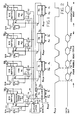
- Fig. 1 is a block diagram of a system according to the invention for rapidly transferring data to and from successive memory locations;
- Fig. 2 depicts waveforms useful in describing the system of Fig. 1;
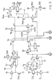
- Fig. 3 is a circuit diagram illustrating the preferred construction of each of the decoders of Fig. 1;
- Fig. 4 is a circuit diagram showing the preferred construction of each of the data input buffers of Fig. 1;
- Fig. 5 is an index relating the signals generated by the circuitry of Fig. 3 to the various decoders of Fig. 1; and
- Fig. 6 illustrates the waveforms of various signals associated with the circuitry of Figs. 3 and 4.
- The present invention causes data stored in successive locations in a semiconductor memory to be rapidly read out of memory in response to a single address input. To achieve this result, the system includes a plurality of N data latches for storing data associated with N successive memory locations. The latter locations are defined by a plurality of bits of the address input.
- To cause the buffers to be sequentially selected for outputting their stored data, a corresponding plurality of N serially connected decoders is included, each decoder being associated with one data latch. In response to the address input, one decoder is enabled for causing its associated data latch to output its stored data. The latter decoder then disabled itself and enables the next decoder so that a second latch outputs its stored data. The process continues with each decoder disabling itself and enabling the next decoder so that the data latches are caused to sequentially output their stored data.
- In the preferred embodiment, rapid writing of data into memory is effected by including N data buffers. The buffers receive incoming data and are adapted to output that data to N successive memory locations when the memory is in its write mode. Each buffer is controlled by one of the decoders which are sequentially enabled as described above. When enabled, a decoder causes its associated buffer to output its data to memory. Hence, the N buffers are sequentially selected to cause the incoming data to be written into N successive memory locations.
- Referring now to Fig. 1, there is shown a system for rapidly reading data from and writing data into successive locations in a semiconductor memory. In the preferred embodiment, "nibble mode" operation is effected whereby four bits of data are read from or written into four successive memory locations in response to a single address input.
- The system includes four data latches, shown as output sense amplifiers A0, A1, A2, and A3, and four decoders D0, D1, D2, and D3, each of the latter being associated with one of the sense amplifiers. The sense amplifiers store four bits of data, one bit per sense amplifier, received from four successive memory locations which are identified by six bits of an eight bit address input. Generally, each of the decoders is adapted to be enabled for causing its associated sense amplifier to output stored data to a
data buss 10 via anoutput latch 12. To initiate the output of data, each decoder receives two bits of the address input such that one of the decoders, DO for example, is enabled in response to the selected two address bits having a given logic state for causing the sense amplifier AO to output a bit of stored data. Then the enabled decoder disables itself and enables a successive decoder, D1 for example, so that its sense amplifier A1 outputs its stored data. The cycle continues with each decoder disabling itself and enabling the next decoder so that the sense amplifiers are enabled in succession. Thus, four bits of data are output to thedata buss 10 in response to a single address input. - As described hereinafter, the decoders DO-D3 are also adapted to be successively enabled for causing four associated data input buffers, BO―B3, to successively apply four bits of input data to four successive locations in memory in response to a single address input. Thus, the illustrated system operates in the "nibble mode" to effect rapid writing of data into memory and rapid reading of data out of memory.
- More specifically, the output sense amplifier AO is adapted to store a data bit and its complement received from a memory location via data busses identified as DBo and DBo. The amplifier A1 is adapted to store a data bit and its complement received from a successive memory location via data busses OB1 and
DB 1. The amplifiers A2 and A3 are likewise adapted to store data bits and their complements received via busses DB2, DB2, and DB3, DB3, respectively. The data bits carried by the busses DB0―DB3 (and their complements) are received from four successive memory locations which are defined by six bits of an eight bit address input to the memory. - The output of the amplifier AO is coupled to the drains of MOS transistors 14 and 16, and the sources of the latter transistors are coupled via
leads output latch 12. Thus, when the transistors 14 and 16 are turned on, the data stored in the amplifier AO is coupled to theoutput buss 10 via thelatch 12. In a similar manner, the amplifiers Al-A3 are coupled to theoutput latch 12 by means oftransistors - The decoder DO receives two selected bits, AO and A1, of the input address via leads 34 and 36. The remaining decoders D1―D3 receive the same address bits, but in different logic combinations, so that only one decoder will be initially selected or enabled. The decoder D1, for example, receives AO and A1, the decoder D2 receives AO and A1 and the decoder D3 receives AO and A1. Thus, when AO and A1 are both at a low logic level, the decoder DO is enabled. Consequently, the decoders D1―D3 are all disabled. However, when the AO and A1 are both at a low logic level, the decoder D1 is enabled and the other decoders are disabled. Suffice it to say that the decoders' input bits will have a given logic state which will enable any one of the decoders DO-D3. The enablement of the remaining decoders is described below.
- The decoders DO-D3 also preferably receive a clock signal identified as φPOF. After a decoder has been selected, the signal φPOF clocks its operation as described below.
- Assuming now that the decoder DO is selected by each of the bits AO and A1 being at a low level, the decoder DO develops an output signal YO when the clock signal (φPOF goes low at time t1, as shown in Fig. 2. The signal YO is coupled via a
lead 38 to the gates of transistors 14 and 16 for turning them on. Hence, the data stored in the amplifier AO is coupled via transistors 14 and 16 to theleads output latch 12, and then to theoutput buss 10. The high or low level data output thus applied to thebuss 10 is represented by DO in Fig. 2. - The decoder DO then disables itself to turn off the transistors 14 and 16 and couples its output signal Y0 to the next successive decoder D1 via a
lead 40. In response to the signal on thelead 40, the decoder D1 is selected so that when the signal φPOF goes low again at time t2 (Fig. 2), it develops an output signal Y1 on lead 42 for turning ontransistors output buss 10. The decoder D1 then disables itself to turn off thetransistors - After the data has been read out of the amplifier A3, the decoder D3 selects the decoder DO via a signal Y3 on a lead 44. Hence, each of the decoders may be selected for another cycle of rapid data reading. Alternately, the nibble read cycle described above may be followed by a conventional read cycle as shown in Fig. 2.
- It should be understood that the nibble mode cycle may start with whatever decoder is first selected by a pair of low logic level input bits. Thereafter, the other decoders are successively selected 'until the four sense amplifiers Ao-A3 have output their stored data.
- To effect a nibble write mode, each of the data input buffers is coupled to associated data busses and receives input data via a pair of transistors which are controlled by one of the decoders. For example, the buffer BO receives an input data bit Din and its complement Din via
transistors transistors DB o. The decoders D1―D3 are then successively enabled as described above for reading three more bits of input data to the remaining busses. In this manner, four bits of input data may be rapidly written into four successive locations in memory. - In Fig. 1, the output sense amplifiers AO-A3 and the
output latch 12 may be conventional. The decoders DO-D3 are all the same, each being preferably constructed as shown in Fig. 3. The buffers BO-B3 are also of the same construction, one of which is shown in Fig. 4. Fig. 6 depicts waveforms of the various input signals, output signals and clock signals associated with the circuitry of Figs. 3 and 4. - Fig. 5 is an index which relates the signals developed by the circuitry of Fig. 3 to the various decoders. For example, where the circuitry of Fig. 3 represents the decoder D0, Y, is the signal YO developed by the decoder D0, and Yi+3 is the signal Y3 developed by the decoder D3. Where the circuitry of Fig. 3 represents the decoder D1, Y; represents the signal Y1 developed by the decoder D1 and Yi+3 represents the signal YO developed by the decoder Y0.
- Referring now to Fig. 3, the illustrated decoder receives its address inputs AO (or AO) and A1 (or
A1 ) at the gates oftransistors transistors - A signal identified as Y,+3 is applied to the gate of a
transistor 60. In the case where the illustrated decoder is D0, the signal Y,+3 is the signal Y3 shown in Fig. 1 and corresponds to the Y, output of the decoder D3. - The illustrated decoder receives a precharge signal φD (see Fig. 6) which is initially high and which is applied to the gate of a
transistor 62 for raising its source (node 64) to a high level. Another clock signal φOD2 (Fig. 6) is also high and is applied to the gate of atransistor 66 which is coupled to thenode 64. Hence, the drain of transistor 66 (node 68) is also driven high. - The signal φD is also applied to the gate of a
transistor 70 forprecharging node 72 to a high level. Consequently,transistors nodes 78 and 80) to a low level. - The gate of another
transistor 82 receives φD for raising the voltage atnode 84 so as to turn ontransistors nodes 90 and 92) to a low level. Atransistor 94 which is coupled to thenode 90 via its gate is thus turned off, as is atransistor 96 whose gate is coupled tonode 92. The source of thetransistor 96 is coupled via a node 98 to atransistor 100 whose gate receives the signal φD. Consequently, the latter transistor is turned on to lower the voltage at the node 98. Atransistor 102 whose gate is also coupled to the node 98 is therefore turned off. The drain of the latter transistor is coupled to thenode 64 but, since the latter transistor is now off, it does not disturb the high level to which thenode 64 is precharged. - The signal φPOF (see Figs. 1 and 6) is high at this time and is applied to a
transistor 104 whose gate is coupled to thenode 78 and whose source is coupled to thenode 80. Because thenode 78 is at a low level, thetransistor 104 is held off and thenode 80 remains at a low level. Thenode 80 is also coupled to the gate of anothertransistor 106 which is also held off at this time. - The signal φPOF is also applied to the
transistor 94. Because the gate of thetransistor 94 is coupled to the low level onnode 90, thetransistor 94 remains off and the potential at its source (node 92) remains low. - Assuming now that the address inputs A0, A1 to the
transistors node 64 remains at a high level as does thenode 68. The latter node is coupled to the gate of a transistor 108 whose drain receives the signal φYO. Because φYO is high (see Fig. 6), the transistor 108 develops a high level output Y, at thelead 54. - The
lead 54 is also coupled to the drain of atransistor 109 whose gate lead 111 is coupled (via a connection which is not shown) to thenode 80. It will be recalled that thenode 80 was pulled low during the precharge cycle. Hence, thetransistor 109 is held off to permit the signal Y, atlead 54 to go high. Thus, in the case where the illustrated decoder represents the decoder DO (Fig. 1), Yi represents YO and the transistors 14 and 16 (Fig. 1) are turned on. All the other decoders are off because at least one of their address inputs is high. Consequently, at least one of the transistors which corresponds totransistors nodes - As stated previously, each of the decoders is adapted to disable itself after its associated sense amplifier has output its stored data. For this purpose, the signal Y, at
lead 54 is coupled to the gate of atransistor 110 via alead 112 and also to the gate oftransistor 58. Consequently,node 84 is pulled low to turn offtransistors transistor 110 is turned on to raise the potential atnode 90 for turning on thetransistor 94. When φPOF goes high again at time Ta (Fig. 6), that high level is coupled to thenode 92 by thetransistor 94. Consequently,transistor 96 turns on to drive the node 98 high, andtransistor 102 turns on for pullingnode 64 low. Hence, the decoder is disabled so that the next time the signal φYO goes high, the output Y; will not be driven high. - Referring briefly to Fig. 6, it can be seen that, when φPOF goes high at time Ta, φYO goes low. The latter signal going low causes the output Y; at
lead 54 to go low also. - Assuming that the operation described above relates to the decoder D0, the latter decoder will enable the decoder D1 for activation by the next high level pulse from φPOF· To explain this phase of the operation, it will now be assumed that the circuitry shown in Fig. 3 represents the decoder D1 (all the decoders are constructed as shown in Fig. 3). Thus, the Yi+3 input to the decoder D1 represents the Y; output of the decoder D0.
- When the Y; output of the decoder DO when high, the Yi+3 input to the decoder D1 was driven high at the gate of the
transistor 60. Hence, thenode 78 was driven high and turned thetransistor 104 on. When φPOF went high at time Ta, thetransistor 104 pulled thenode 80 high and turned ontransistor 106. Because the source of thetransistor 106 is coupled to thenode 64, the latter node was driven high. φ0D2 also went high at time Ta. Hence, thenode 68 was also pulled high. But because φYO went low then, the transistor 108 held the Y, output of the decoder D1 at a low level. However, when φYO goes high at time tb (Fig. 6), the Y; output atlead 54 is pulled high. - The operation described above continues for each nibble cycle so that the ith decoder primes the ith plus 1 decoder to fire when φYO goes high.
- Each decoder also includes an active hold off circuit coupled to the Y; output lead 54. This circuit includes
transistors - The gates of
transistors 114 and 120 each receive the φPOF signal, wherefore their sources (nodes 122 and 124) are pulled to a high level during the precharge cycle. The gate oftransistor 118 receives the φYO signal so that, when that signal goes high, the drain of transistor 118 (node 124) is pulled low. - If
node 64 is low (indicating that the decoder is not selected), thetransistor 116 remains off and thenode 122 remains high. Consequently, thetransistor 112 is turned on to hold thelead 54 at ground potential. - In the case in which the
node 64 is high, thetransistor 116 is turned on to pullnode 122 low and hold thetransistor 112 off to permit thelead 54 to be driven to a high level. - Referring now to Fig. 4, a data input buffer is shown whose construction is preferably of the type used for each of the buffers B0―B3 of Fig. 1. The illustrated buffer includes input leads 126 and 128 for receiving externally applied Din and
Din data inputs and output leads 130 and 132 which couple DB, and DB, outputs to the data busses (such as DBo and DBo) of Fig. 1. Other inputs include leads 134 and 136 which couple tonode 64 of Fig. 3, lead 138 which couples tonode 80 of Fig. 3, and lead 140 which couples tonode 92 of Fig. 3. As described in detail below, an enabled decoder activates its associated buffer to cause the latter to couple the data input (Din and Din) to the DB, and DB, outputs. - When the decoder which is associated with the illustrated buffer is not enabled, the potential at the decoder's
node 64 is low. That low level potential is coupled via thelead 134 totransistors 142 and 14 whose gates receive the signal (φOD2· Consequently, the sources (nodes 146 and 148) oftransistors -
Nodes transistors 150 and 152 which receive the Din and Din inputs. Withnodes - When the decoder which is associated with the illustrated buffer is enabled, the potential at the decoder's
node 64 is high. Consequently,buffer nodes transistors 150 and 152 are turned on. In the case where the Din input is high and the Din input is low, the sources oftransistors 150 and 152 (nodes 154 and 156) are driven high and low, respectively. - The
node 154 is coupled to the gates oftransistors node 156 is coupled to the gates oftransistors transistors transistors lead 130 is driven to a high level and thelead 132 is driven to a low level. The data coupled toleads - It will be appreciated that writing data into memory is a relatively time consuming operation. Therefore, the data output from the illustrated buffer is held available for reading even after the next successive decoder and buffer are enabled on the next nibble cycle. Toward this end,
transistors nodes - The gates of
transistors node 92 in Fig. 3. The latter node is driven to a high level when φPOF goes high at the beginning of a nibble cycle. Consequently,transistors transistors 150 and 152, the latter transistors are turned off. Thus, the high and low levels previously applied tonodes transistors transistors leads - The illustrated buffer also preferbaly includes a pair of active hold off circuits to hold the buffer insensitive to further data inputs when its associated decoder is disabled. The first hold off circuit includes
transistors transistors - Referring to the first hold off circuit, the gates of
transistors 174 and 180 receive the signal φD forprecharging nodes lead 202 to the gate of transistor 182 so that, when Din is high,node 200 is pulled low. - The gate of
transistor 176 is coupled vialead 136 tonode 64 in Fig. 3, its source is coupled tonode 200, and its drain is coupled tonode 198. Thus, if the buffer's decoder is enabled,node 64 is high,transistor 176 is on, andnode 198 is pulled low. Hence,transistor 183 is turned off and the potential at its drain (node 154) is allowed to vary in response to the Din input atlead 126. - If the illustrated buffer's decoder had been disabled,
node 64 in that decoder would be low, whereforetransistor 176 would be off andnode 198 would be at a high level. Consequently,transistor 183 would be on to pull thenode 154 to ground potential. - The other hold off circuit operates in a manner similar to that described above. Suffice it to say that when the buffer's decoder is enabled, the
transistor 196 remains off to allownode 156 to vary in response to the Din input atlead 128. Otherwise,transistor 196 is on to holdnode 156 at ground potential. - It is often desirable to write a full Vcc voltage into memory locations. In the present embodiment,
nodes capacitors 204 and 206 which are coupled tonodes nodes - Another feature which improves the speed of the system is the use of φOD2. As shown in Fig. 6, ooo2 generally follows φPOF, but φOD2 varies between 7 volts and 4 volts whereas φPOF varies between 5 volts and zero volts. The use of φOD2 considerably shortens the precharge portion of the nibble cycle as demonstrated by the comments below.
- It will be understood that it is desirable to drive the signal Yj (at lead 54) up to Vcc (five volts, for example). To do this, the voltage at
lead 68 is driven higher than Vcc, preferably toward seven volts, in the following manner. Referring to Figure 6, it can be seen that (POD2 drops from seven volts to four volts just prior to φYO going high at time tb. - Just prior to that occurrence, φPOF had been high toprecharge node 64 to about four volts viatransistors transistor 66 has four volts at its gate and about four volts at its source. In this state, thetransistor 66 is cut off, thereby releasing or isolatingnode 68 fromnode 64. Accordingly, when φYO goes high to raise the voltage at the drain of transistor 108,node 68 is bootstrapped to above seven volts by the gate-to- drain capacity of the transistor and Y, is driven high. Hadtransistor 66 not been cut off by φOD2, node 68 would not have been released from thenode 64, no such bootstrapping would have occurred, and the signal Y, would not have been driven to as high a level as is desired. - It will be appreciated that the
transistor 66 could have been cut off by causingnode 64 to be precharged to a higher level. However, the additional time required for such precharging to occur would lengthen the time required to enable the decoder. With the illustrated arrangement, the decoder's enabling time is kept short while still retaining the ability to bootstrap thenode 68 and drive the signal Y, up to Vcc. - An arrangement utilizing φOD2 in a similar manner is shown in Figure 4 in which
buffer nodes node 64 when φOD2 falls to four volts, thereby permitting efficient bootstrapping to occur atnodes - The present system may be used with a pair of memories, each of which operate in the nibble mode. Conventionally, each such memory is controlled by RAS and CAS clocks to define the precharge and active (read or write) cycles. A first memory may have RAS and CAS going low to initiate a nibble read (or write) cycle while a second memory is in a prechagge mode. Then the RAS and CAS clocks in the first memory may be driven high to precharge the first memory while RAS and CAS in the second memory go low to initiate a nibble read cycle therein. By so staggering the RAS and CAS clocks for both memories, a bit of data may be read for each nibble cycle for an indefinite period of time.
- One of the advantages of the illustrated decoder and buffer is that virtually no D.C. power is consumed and reliable operation is obtained at low precharge voltages. Of course, very high speed operation is obtained by virtue of each decoder disabling itself and enabling a successive decoder. In addition, input data is easily and rapidly read by virtue of the fact that each buffer maintains the status of its data outputs through four nibble cycles.
- Although the invention has been described in terms of a preferred embodiment, it will be obvious to those skilled in the art that many modifications and alterations may be made without departing from the invention. Accordingly, it is intended that all such modifications and alterations be considered as within the scope of the invention as defined by the appended claims.
Claims (7)
Applications Claiming Priority (2)
| Application Number | Priority Date | Filing Date | Title |
|---|---|---|---|
| US06/195,729 US4344156A (en) | 1980-10-10 | 1980-10-10 | High speed data transfer for a semiconductor memory |
| US195729 | 1994-02-14 |
Publications (3)
| Publication Number | Publication Date |
|---|---|
| EP0049988A2 EP0049988A2 (en) | 1982-04-21 |
| EP0049988A3 EP0049988A3 (en) | 1983-09-28 |
| EP0049988B1 true EP0049988B1 (en) | 1988-04-27 |
Family
ID=22722545
Family Applications (1)
| Application Number | Title | Priority Date | Filing Date |
|---|---|---|---|
| EP81304605A Expired EP0049988B1 (en) | 1980-10-10 | 1981-10-05 | High speed data transfer for a semiconductor memory |
Country Status (5)
| Country | Link |
|---|---|
| US (1) | US4344156A (en) |
| EP (1) | EP0049988B1 (en) |
| JP (1) | JPS5792473A (en) |
| CA (1) | CA1161956A (en) |
| DE (1) | DE3176726D1 (en) |
Families Citing this family (53)
| Publication number | Priority date | Publication date | Assignee | Title |
|---|---|---|---|---|
| US4556961A (en) * | 1981-05-26 | 1985-12-03 | Tokyo Shibaura Denki Kabushiki Kaisha | Semiconductor memory with delay means to reduce peak currents |
| JPS57210495A (en) * | 1981-06-10 | 1982-12-24 | Nec Corp | Block access memory |
| US4480320A (en) * | 1982-06-01 | 1984-10-30 | General Instrument Corp. | Compact ROM with reduced access time |
| US4484308A (en) * | 1982-09-23 | 1984-11-20 | Motorola, Inc. | Serial data mode circuit for a memory |
| JPS5961152A (en) * | 1982-09-30 | 1984-04-07 | Fujitsu Ltd | Semiconductor device |
| US4586167A (en) * | 1983-01-24 | 1986-04-29 | Mitsubishi Denki Kabushiki Kaisha | Semiconductor memory device |
| JPS59135695A (en) * | 1983-01-24 | 1984-08-03 | Mitsubishi Electric Corp | Semiconductor storage device |
| US4567579A (en) * | 1983-07-08 | 1986-01-28 | Texas Instruments Incorporated | Dynamic memory with high speed nibble mode |
| JPS6072020A (en) * | 1983-09-29 | 1985-04-24 | Nec Corp | Dual port memory circuit |
| JPS60117492A (en) * | 1983-11-29 | 1985-06-24 | Fujitsu Ltd | Semiconductor memory device |
| JPS60136086A (en) * | 1983-12-23 | 1985-07-19 | Hitachi Ltd | Semiconductor memory device |
| GB8401804D0 (en) * | 1984-01-24 | 1984-02-29 | Int Computers Ltd | Data storage apparatus |
| JPH0787037B2 (en) * | 1984-03-02 | 1995-09-20 | 沖電気工業株式会社 | Data writing method of semiconductor memory circuit |
| JPH0799616B2 (en) * | 1984-08-30 | 1995-10-25 | 三菱電機株式会社 | Semiconductor memory device |
| US4719602A (en) * | 1985-02-07 | 1988-01-12 | Visic, Inc. | Memory with improved column access |
| US4630239A (en) * | 1985-07-01 | 1986-12-16 | Motorola, Inc. | Chip select speed-up circuit for a memory |
| JPS639096A (en) * | 1986-06-30 | 1988-01-14 | Toshiba Corp | Semiconductor memory |
| JPS6363200A (en) * | 1986-09-03 | 1988-03-19 | Mitsubishi Electric Corp | semiconductor storage device |
| EP0262413B1 (en) * | 1986-09-04 | 1992-07-22 | Fujitsu Limited | Memory device employing address multiplexing |
| JPS63136267U (en) * | 1987-02-26 | 1988-09-07 | ||
| US5245566A (en) * | 1987-04-24 | 1993-09-14 | Fujio Masuoka | Programmable semiconductor |
| US5313420A (en) | 1987-04-24 | 1994-05-17 | Kabushiki Kaisha Toshiba | Programmable semiconductor memory |
| JPH0752583B2 (en) * | 1987-11-30 | 1995-06-05 | 株式会社東芝 | Semiconductor memory |
| JPH01175314A (en) * | 1987-12-29 | 1989-07-11 | Nec Corp | Input inverter circuit |
| JPS63132893U (en) * | 1988-01-08 | 1988-08-30 | ||
| US5267200A (en) * | 1988-08-31 | 1993-11-30 | Mitsubishi Denki Kabushiki Kaisha | Semiconductor memory device and operating method thereof with transfer transistor used as a holding means |
| EP0388175B1 (en) * | 1989-03-15 | 1995-11-02 | Matsushita Electronics Corporation | Semiconductor memory device |
| DE4114744C1 (en) * | 1991-05-06 | 1992-05-27 | Siemens Ag, 8000 Muenchen, De | |
| US6091639A (en) * | 1993-08-27 | 2000-07-18 | Kabushiki Kaisha Toshiba | Non-volatile semiconductor memory device and data programming method |
| US5506809A (en) * | 1994-06-29 | 1996-04-09 | Sharp Kabushiki Kaisha | Predictive status flag generation in a first-in first-out (FIFO) memory device method and apparatus |
| US5640364A (en) * | 1994-12-23 | 1997-06-17 | Micron Technology, Inc. | Self-enabling pulse trapping circuit |
| US5729503A (en) * | 1994-12-23 | 1998-03-17 | Micron Technology, Inc. | Address transition detection on a synchronous design |
| US5598376A (en) * | 1994-12-23 | 1997-01-28 | Micron Technology, Inc. | Distributed write data drivers for burst access memories |
| US5668773A (en) * | 1994-12-23 | 1997-09-16 | Micron Technology, Inc. | Synchronous burst extended data out DRAM |
| US6804760B2 (en) | 1994-12-23 | 2004-10-12 | Micron Technology, Inc. | Method for determining a type of memory present in a system |
| US5675549A (en) * | 1994-12-23 | 1997-10-07 | Micron Technology, Inc. | Burst EDO memory device address counter |
| US5652724A (en) * | 1994-12-23 | 1997-07-29 | Micron Technology, Inc. | Burst EDO memory device having pipelined output buffer |
| US5526320A (en) * | 1994-12-23 | 1996-06-11 | Micron Technology Inc. | Burst EDO memory device |
| US5682354A (en) * | 1995-11-06 | 1997-10-28 | Micron Technology, Inc. | CAS recognition in burst extended data out DRAM |
| US6525971B2 (en) | 1995-06-30 | 2003-02-25 | Micron Technology, Inc. | Distributed write data drivers for burst access memories |
| US5610864A (en) * | 1994-12-23 | 1997-03-11 | Micron Technology, Inc. | Burst EDO memory device with maximized write cycle timing |
| US5721859A (en) * | 1994-12-23 | 1998-02-24 | Micron Technology, Inc. | Counter control circuit in a burst memory |
| US5717654A (en) * | 1995-02-10 | 1998-02-10 | Micron Technology, Inc. | Burst EDO memory device with maximized write cycle timing |
| US5850368A (en) * | 1995-06-01 | 1998-12-15 | Micron Technology, Inc. | Burst EDO memory address counter |
| JP2900854B2 (en) * | 1995-09-14 | 1999-06-02 | 日本電気株式会社 | Semiconductor storage device |
| US5729504A (en) * | 1995-12-14 | 1998-03-17 | Micron Technology, Inc. | Continuous burst edo memory device |
| US5966724A (en) * | 1996-01-11 | 1999-10-12 | Micron Technology, Inc. | Synchronous memory device with dual page and burst mode operations |
| US7681005B1 (en) | 1996-01-11 | 2010-03-16 | Micron Technology, Inc. | Asynchronously-accessible memory device with mode selection circuitry for burst or pipelined operation |
| US6401186B1 (en) | 1996-07-03 | 2002-06-04 | Micron Technology, Inc. | Continuous burst memory which anticipates a next requested start address |
| US6981126B1 (en) | 1996-07-03 | 2005-12-27 | Micron Technology, Inc. | Continuous interleave burst access |
| JPH10124447A (en) * | 1996-10-18 | 1998-05-15 | Fujitsu Ltd | Data transfer control method and device |
| US7103742B1 (en) | 1997-12-03 | 2006-09-05 | Micron Technology, Inc. | Burst/pipelined edo memory device |
| US7927948B2 (en) | 2005-07-20 | 2011-04-19 | Micron Technology, Inc. | Devices with nanocrystals and methods of formation |
Citations (1)
| Publication number | Priority date | Publication date | Assignee | Title |
|---|---|---|---|---|
| EP0045063A2 (en) * | 1980-07-23 | 1982-02-03 | Nec Corporation | Memory device |
Family Cites Families (8)
| Publication number | Priority date | Publication date | Assignee | Title |
|---|---|---|---|---|
| US3857046A (en) * | 1970-11-04 | 1974-12-24 | Gen Instrument Corp | Shift register-decoder circuit for addressing permanent storage memory |
| US3771145B1 (en) * | 1971-02-01 | 1994-11-01 | Wiener Patricia P. | Integrated circuit read-only memory |
| NL7309642A (en) * | 1973-07-11 | 1975-01-14 | Philips Nv | INTEGRATED MEMORY. |
| DE2712735B1 (en) * | 1977-03-23 | 1978-09-14 | Ibm Deutschland | Read / write access circuit to memory cells of a memory and method for their operation |
| JPS5410412A (en) * | 1977-06-23 | 1979-01-26 | Kyokuto Kikai Seisakusho:Kk | Low noise multi-stage axial flow blower |
| US4254477A (en) * | 1978-10-25 | 1981-03-03 | Mcdonnell Douglas Corporation | Reconfigurable memory circuit |
| US4279023A (en) * | 1979-12-19 | 1981-07-14 | International Business Machines Corporation | Sense latch |
| JPS6118837A (en) * | 1984-07-06 | 1986-01-27 | Yaskawa Electric Mfg Co Ltd | wave making device |
-
1980
- 1980-10-10 US US06/195,729 patent/US4344156A/en not_active Expired - Lifetime
-
1981
- 1981-03-17 CA CA000373194A patent/CA1161956A/en not_active Expired
- 1981-10-05 DE DE8181304605T patent/DE3176726D1/en not_active Expired
- 1981-10-05 EP EP81304605A patent/EP0049988B1/en not_active Expired
- 1981-10-05 JP JP56158570A patent/JPS5792473A/en active Granted
Patent Citations (1)
| Publication number | Priority date | Publication date | Assignee | Title |
|---|---|---|---|---|
| EP0045063A2 (en) * | 1980-07-23 | 1982-02-03 | Nec Corporation | Memory device |
Also Published As
| Publication number | Publication date |
|---|---|
| CA1161956A (en) | 1984-02-07 |
| EP0049988A2 (en) | 1982-04-21 |
| DE3176726D1 (en) | 1988-06-01 |
| JPS5792473A (en) | 1982-06-09 |
| US4344156A (en) | 1982-08-10 |
| EP0049988A3 (en) | 1983-09-28 |
| JPS6129069B2 (en) | 1986-07-04 |
Similar Documents
| Publication | Publication Date | Title |
|---|---|---|
| US4344156A (en) | High speed data transfer for a semiconductor memory | |
| US6105106A (en) | Computer system, memory device and shift register including a balanced switching circuit with series connected transfer gates which are selectively clocked for fast switching times | |
| EP0135940B1 (en) | Dual port memory circuit | |
| US5155705A (en) | Semiconductor memory device having flash write function | |
| US6175533B1 (en) | Multi-port memory cell with preset | |
| KR900007226B1 (en) | Semiconductor memory device | |
| US5544101A (en) | Memory device having a latching multiplexer and a multiplexer block therefor | |
| EP0017228B1 (en) | Memory device | |
| JPS61160898A (en) | Semiconductor memory device | |
| JPH08195085A (en) | Sense amplification in data memory | |
| US5235543A (en) | Dual port static memory with one cycle read-modify-write | |
| JPH0146951B2 (en) | ||
| JPH0642313B2 (en) | Semiconductor memory | |
| JPS6249676B2 (en) | ||
| JPH028399B2 (en) | ||
| JPH06139776A (en) | Semiconductor memory device | |
| JPH1166850A (en) | Semiconductor storage device | |
| US6188623B1 (en) | Voltage differential sensing circuit and methods of using same | |
| EP0199458A2 (en) | Memory circuit having an improved writing scheme | |
| KR970005411B1 (en) | A read/write memory with selective row write capability | |
| JP3000297B2 (en) | memory | |
| JPS6216472B2 (en) | ||
| JP2826238B2 (en) | Semiconductor memory | |
| JPS60119691A (en) | Memory circuit | |
| US4870616A (en) | Compact register set using a psram array |
Legal Events
| Date | Code | Title | Description |
|---|---|---|---|
| PUAI | Public reference made under article 153(3) epc to a published international application that has entered the european phase |
Free format text: ORIGINAL CODE: 0009012 |
|
| AK | Designated contracting states |
Designated state(s): DE FR GB NL |
|
| PUAL | Search report despatched |
Free format text: ORIGINAL CODE: 0009013 |
|
| AK | Designated contracting states |
Designated state(s): DE FR GB NL |
|
| 17P | Request for examination filed |
Effective date: 19831112 |
|
| GRAA | (expected) grant |
Free format text: ORIGINAL CODE: 0009210 |
|
| AK | Designated contracting states |
Kind code of ref document: B1 Designated state(s): DE FR GB NL |
|
| REF | Corresponds to: |
Ref document number: 3176726 Country of ref document: DE Date of ref document: 19880601 |
|
| ET | Fr: translation filed | ||
| PLBE | No opposition filed within time limit |
Free format text: ORIGINAL CODE: 0009261 |
|
| STAA | Information on the status of an ep patent application or granted ep patent |
Free format text: STATUS: NO OPPOSITION FILED WITHIN TIME LIMIT |
|
| 26N | No opposition filed | ||
| ITCP | It: supplementary protection certificate |
Spc suppl protection certif: CCP 415 |
|
| PGFP | Annual fee paid to national office [announced via postgrant information from national office to epo] |
Ref country code: FR Payment date: 20000918 Year of fee payment: 20 |
|
| PGFP | Annual fee paid to national office [announced via postgrant information from national office to epo] |
Ref country code: GB Payment date: 20000921 Year of fee payment: 20 |
|
| PGFP | Annual fee paid to national office [announced via postgrant information from national office to epo] |
Ref country code: NL Payment date: 20000925 Year of fee payment: 20 |
|
| PGFP | Annual fee paid to national office [announced via postgrant information from national office to epo] |
Ref country code: DE Payment date: 20001229 Year of fee payment: 20 |
|
| PG25 | Lapsed in a contracting state [announced via postgrant information from national office to epo] |
Ref country code: GB Free format text: LAPSE BECAUSE OF EXPIRATION OF PROTECTION Effective date: 20011004 |
|
| PG25 | Lapsed in a contracting state [announced via postgrant information from national office to epo] |
Ref country code: NL Free format text: LAPSE BECAUSE OF EXPIRATION OF PROTECTION Effective date: 20011005 |
|
| REG | Reference to a national code |
Ref country code: GB Ref legal event code: PE20 Effective date: 20011004 |
|
| NLV7 | Nl: ceased due to reaching the maximum lifetime of a patent |
Effective date: 20011005 |