EP0049630B1 - Dummy cell arrangement for an mos memory - Google Patents
Dummy cell arrangement for an mos memory Download PDFInfo
- Publication number
- EP0049630B1 EP0049630B1 EP81304604A EP81304604A EP0049630B1 EP 0049630 B1 EP0049630 B1 EP 0049630B1 EP 81304604 A EP81304604 A EP 81304604A EP 81304604 A EP81304604 A EP 81304604A EP 0049630 B1 EP0049630 B1 EP 0049630B1
- Authority
- EP
- European Patent Office
- Prior art keywords
- dummy
- capacitor
- bit lines
- coupled
- lines
- Prior art date
- Legal status (The legal status is an assumption and is not a legal conclusion. Google has not performed a legal analysis and makes no representation as to the accuracy of the status listed.)
- Expired
Links
- 230000015654 memory Effects 0.000 title claims description 84
- 239000003990 capacitor Substances 0.000 claims description 112
- 230000004044 response Effects 0.000 claims description 9
- 230000008878 coupling Effects 0.000 claims description 8
- 238000010168 coupling process Methods 0.000 claims description 8
- 238000005859 coupling reaction Methods 0.000 claims description 8
- 230000000694 effects Effects 0.000 claims description 6
- 210000004027 cell Anatomy 0.000 description 89
- 230000008859 change Effects 0.000 description 4
- 238000004519 manufacturing process Methods 0.000 description 3
- 230000008901 benefit Effects 0.000 description 2
- 230000004075 alteration Effects 0.000 description 1
- 230000009286 beneficial effect Effects 0.000 description 1
- 239000011159 matrix material Substances 0.000 description 1
- 229910044991 metal oxide Inorganic materials 0.000 description 1
- 150000004706 metal oxides Chemical class 0.000 description 1
- 238000012986 modification Methods 0.000 description 1
- 230000004048 modification Effects 0.000 description 1
- 239000004065 semiconductor Substances 0.000 description 1
- 210000000352 storage cell Anatomy 0.000 description 1
Images
Classifications
-
- G—PHYSICS
- G11—INFORMATION STORAGE
- G11C—STATIC STORES
- G11C11/00—Digital stores characterised by the use of particular electric or magnetic storage elements; Storage elements therefor
- G11C11/21—Digital stores characterised by the use of particular electric or magnetic storage elements; Storage elements therefor using electric elements
- G11C11/34—Digital stores characterised by the use of particular electric or magnetic storage elements; Storage elements therefor using electric elements using semiconductor devices
- G11C11/40—Digital stores characterised by the use of particular electric or magnetic storage elements; Storage elements therefor using electric elements using semiconductor devices using transistors
- G11C11/401—Digital stores characterised by the use of particular electric or magnetic storage elements; Storage elements therefor using electric elements using semiconductor devices using transistors forming cells needing refreshing or charge regeneration, i.e. dynamic cells
- G11C11/4063—Auxiliary circuits, e.g. for addressing, decoding, driving, writing, sensing or timing
- G11C11/407—Auxiliary circuits, e.g. for addressing, decoding, driving, writing, sensing or timing for memory cells of the field-effect type
- G11C11/409—Read-write [R-W] circuits
- G11C11/4099—Dummy cell treatment; Reference voltage generators
Definitions
- the present invention relates generally to improvements in MOS (metal oxide semiconductor) memories, and in particular to a so-called "dummy cell" arrangement for sensing the logic state of a memory cell.
- MOS metal oxide semiconductor
- logical data is stored in a matrix of memory cells, each of which includes a cell capacitor for storing a charge which indicates whether its cell is in a logic 1 or a logic 0 state.
- a large number of such memory cells are typically associated with each of the memory's bit lines.
- US-A-4,136,401 describes a memory in which a number of "dummy cells" are also included. Each of these dummy cells is identical to each of the memory cells but the dummy cells are precharged to a voltage which lies between the "zero" signal level and the "one" signal level of the storage cells.
- each dummy cell includes a dummy capacitor which is conventionally one-half the size of a memory cell capacitor and which is precharged to a reference voltage level.
- the charge on the memory's cell capacitor is dumped on a first bit line and the charge on the dummy cell's capacitor is dumped on a second bit line.
- the resultant difference in voltage on the two bit lines is used as an indication of whether the memory cell is in a logic 1 or a logic 0 state.
- a drawback of this known dummy cell arrangement described above is that, as memory cell capacitors are reduced in size, it is difficult to build a dummy cell capacitor which is one-halfthe . size of the memory cell capacitor. Manufacturing variables which cause the size of the memory cell capacitor to vary by a given amount generally result in a similar change in the size of the dummy capacitor rather than one-half the change. Hence, their two-to-one size relationship changes.
- an MOS memory comprising a plurality of memory cells each having a memory cell capacitor of a predetermined size arranged to be charged so as to reflect the logic state of its memory cell, a plurality of bit lines and word lines for accessing selected memory cells, a dummy cell arrangement comprising a dummy cell having a dummy capacitor having substantially the same predetermined size as that of a memory cell capacitor and arranged to be precharged to a selected voltage level and means for selectively coupling the capacitor associated with the accessed memory cell to a first bit line so as to effect a transfer of charge between the first bit line and the memory cell capacitor for changing the voltage on the first bit line, characterised in that means are provided for selectively coupling or decoupling the dummy capacitor to second and third bit lines simultaneously such that the capacitance associated with the dummy capacitor effects substantially equal transfers of charge between the second and third bit lines and the dummy capacitor, thereby imparting voltage changes to the second and third bit lines, and means for sensing a difference in voltage
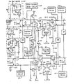
- a representative portion of a dynamic MOS memory which includes a preferred form of a dummy cell arrangement.
- the illustrated structure includes four pair of bit lines identified as A-B, C-D, E-F and G-H.
- the pair of bit lines A-B is coupled through transistors 10 and 12 to a sense amplifier 14.
- a second pair of bit lines C-D is similarly coupled to the sense amplifier 14.
- the sense amplifier 14 is adapted to sense the potentials on bit lines A and B or on bit lines C and D.
- the bit line pairs E-F and G-H are connected in a similar arrangement with another sense amplifier.
- one of the bit lines (A, for example) is coupled to a capacitor associated with an addressed memory cell so that a charge transfer occurs between that bit line and the latter capacitor.
- the other bit line in that pair (B, for example) carries a reference voltage induced by a dummy cell capacitor.
- the sense amplifier 14 detects the voltage difference between both bit lines and latches in a state which is indicative of the state of the addressed memory cell.
- the sense amplifier 14 includes transistors 16 and 18 which are interconnected as a flip-flop. As shown, the source of the transistors 12 is coupled to the drain of the transistor 16 and to the gate of the transistor 18. The source of the transistor 10 is coupled to the drain of the transistor 18 and to the gate of the transistor 16.
- the bit lines C and D are coupled via transistors 20 and 22 to the sense amplifier 14 such that the source of the transistor 20 is coupled to the drain of transistor 16 and to the gate of transistor 18, and such that the source of transistor 22 is coupled to the drain of transistor 18 and to the gate of transistor 16.
- either the transistor pair 10-12 or the transistor pair 20-22 may be turned on to couple the sense amplifier either to bit lines A and B or to bit lines C and D.
- the amplifier 14 When the amplifier 14 is enabled by a low level latch signal applied to the sources of transistors 16 and 18, the amplifier detects the voltage differential between the bit lines A and B (or C and D) and latches in a state indicative of the logic level associated with an addressed memory cell which feeds one of the bit lines.
- Shown coupled to the bit line A is an exemplary memory cell M1 which includes a transistor 24 and a memory cell capacitor C M . As is conventional, this capacitor stores a charge which is indicative of the logic state of the cell M1.
- a word line 26 is driven to a high level when the cell M1 is addressed so as to turn on the transistor 24 and thereby couple the capacitor C m to the bit line A.
- Additional memory cells 28, each similar to the cell M1, are also associated with the bit line A and may be coupled thereto when addressed by their own word lines.
- memory cells groups 29, 30 and 32 are associated with bit lines B, C, and D, respectively, and may be selectively coupled to their associated bit lines when addressed by their own word lines.
- bit lines E and F are associated with groups of memory cells 34 and 35, respectively, and are coupled to a sense amplifier 36 via transistors 37 and 38.
- Bit lines G and H are associated with groups of memory cells 40 and 42, respectively, and are coupled to the sense amplifier 36 (constructed similarly to the sense amplifier 14) via transistors 44 and 46. Suffice it to say that the groups 34, 35, 40 and 42 of memory cells all contain individual memory cells similar to the memory cell M1 and are addressed in a similar manner.
- the sense amplifier 36 senses the voltage differential between bit lines E and F or between the bit lines G and H, depending on whether transistors 36-38 are energized or whether transistors 44-46 are energized.
- a clock signal indicated as ⁇ RPL is coupled via leads 48 and 50 to the gates of transistors 10, 12, 37 and 38, and another clock signal indicated as ⁇ RPR is coupled via leads 52 and 54 to the gates of transistors 20, 22, 44 and 46.
- the clock signal (P RPR is brought low and the clock signal ⁇ RPL is held high (above Vcc). Consequently, transistors 10 and 12 are turned on to couple the bit lines A and B to the sense amplifier 14, and transistors 37 and 38 are turned on for coupling the bit lines E and F to the sense amplifier 36.
- Transistors 20, 22, 44 and 46 are, of course, held off to decouple the bit lines C, D, G and H from the sense amplifiers 14 and 36.
- the memory cell M1 its memory capacitor C m is coupled to the bit line A via the transistor 24.
- a transfer of charge occurs between the latter capacitor and the bit line A, thereby altering the voltage level on that bit line.
- a dummy capacitor of the same size as the capacitor C M and precharged to a selected voltage level, is coupled to the bit line B and to another bit line (F, for example) such that the capacitance associated with the dummy capacitor effects substantially equal transfers of charge between itself and the bit lines to which it is coupled.
- the charge of the dummy capacitor is split between both bit lines.
- the voltage on the bit line A is compared by the sense amplifier 14 with the voltage on the bit line B to determine the logic state of the memory cell M1.
- a dummy cell D1 is shown coupled between bit line B and F via leads 56 and 58.
- the cell D1 includes a dummy cell capacitor C o whose size is selected to be substantially equal to the size of the memory cell capacitor C M .
- the capacitor C D is adapted to be coupled to the bit line B by a transistor 60, and is adapted to be coupled to the bit line F by another transistor 62.
- the latter transistors are turned on simultaneously when a high level signal is applied to a dummy word line 64.
- a transistor 66 has its drain coupled to the capacitor C D , its source coupled to ground, and its gate coupled to a precharge line 68. Thus, when the line 68 is driven high, the transistor 66 conducts to precharge the capacitor C D to zero volts.
- a dummy cell D2 similar to the dummy cell D1, and activated by its own precharge and word lines (not shown), is coupled between the bit lines A and E.
- similar dummy cells D3 and D4 are coupled between bit lines D-H and C-G, respectively.
- transistors 70 and 72 may be coupled between bit line pairs A-B and E-F, respectively, for shorting together bit lines A and B and bit lines E and F in response to a clock signal designated as ⁇ SH ⁇
- a transistor 74 is coupled to Vcc via its drain, to the bit line A via its source, and to precharge clock signal (P L via its gate.
- P L precharge clock signal
- bit lines B, E and F are precharged by transistors 76, 78 and 80 in response to the signal ⁇ L .
- bit lines C, D, G and H will also normally be coupled to precharging and equilibrating transistors (not shown) in the manner as bit lines A, B, E and F.
- the clock signal ⁇ SH is first driven high to turn on the transistors 70 and 72 so that the bit line pairs A-B and E-F are equilibrated.
- the clock signal ⁇ L is then driven high to turn on the transistors 74, 76, 78 and 80 so that bit lines A, B, E and F are precharged to a voltage near Vcc.
- the dummy precharge line 68 is also driven high to ensure that the voltage across the capacitor C D is equal to zero.
- the memory drives the word line 26 high to turn on the transistor 24 and couple the capacitor C M to the bit line A. (Another word line will ordinarily be driven high to couple another memory capacitor in the group 34 to the bit line E).
- the dummy word line 64 is driven high to turn on the transistors 60 and 62, thereby coupling the capacitor C o to the bit lines B and F.
- the clock signal (P RPL is held high while the clock signal ⁇ RPR is driven low. Consequently, the transistors 10 and 12 conduct to couple the bit lines A and B to the sense amplifier 14.
- the latter amplifier is enabled by the negative-going latch signal received at the sources of transistors 16 and 18.
- Vcc equals 5 volts
- all bit lines are precharged to 5 volts
- the voltage across the capacitor C M equals zero volts.
- the voltage across the dummy cell capacitor C o is also equal to zero volts.
- the capacitor C M When the capacitor C M is coupled to the bit line A, the voltage on the latter bit line drops to about 4.8 volts.
- the capacitor C D When the capacitor C D is coupled to bit lines B and F, the voltage on those bit lines drops only to about 4.9 volts because the charge on capacitor C o is equally divided between the bit lines B and F.
- the transistor 18 When the sense amplifier 14 is enabled by the low level latch signal, the transistor 18 turns on before transistor 16 because its gate voltage (4.9 volts) is higher than the voltage (4.8 volts) on the gate of transistor 16. Consequently, the voltage at the drain of transistor 18 (node 82) is pulled low (to about zero volts) and the voltage at the drain of transistor 16 (node 84) remains high (at 4.9 volts). Thus, the one tenth volt differential between bit lines A and B has been converted by the sense amplifier 14 to almost a 5 volt differential between nodes 82 and 84. This differential voltage, indicative of the memory cell M1 being in a logic zero state, may be coupled to data lines (not shown) in the usual manner.
- the sense amplifier 36 detects the voltage differential between bit lines E and F in the manner described above. Specifically, if the addressed memory cell in the group 34 is in a logic zero state while the capacitor C D lowers the voltage on bit line F to about 4.9 volts, the sense amplifier 36 generates a low level signal at its node 86 and a high level signal at its node 88. Conversely, if the addressed memory cell is in a logic 1 state, the amplifier 36 generates a high level signal at node 86 and a low level signal at node 88. Both such nodes may be coupled to another pair of data lines in the conventional manner.
- a primary advantage of the illustrated dummy cell arrangement is that each dummy cell capacitor is as large as each memory cell capacitor. Hence, the problems associated with manufacturing a half size dummy capacitor are avoided.
- Another advantage resides in the fact that manufacturing variables which tend to change the size of the memory cell capacitors will change the size of the dummy cell capacitors by the same percentage. Hence, the 1:1 size relationship between the dummy cell capacitors and the memory cell capacitors is maintained.
- Another factor to be considered in the design of a dummy cell is the total charge transfer which occurs between the dummy cell capacitor and its bit line, on the one hand, and between the memory cell capacitor and its bit line, on the other hand.
- a charge of Q will be transferred between the capacitor C M and the bit line A while a charge of one-half Q will be transferred between the capacitor C D and the bit line B (Q equals the value of the capacitor C M times the voltage to which it becomes charged).
- a 2:1 ratio in such charge transfer is effected by applying the same high level potential, 5 volts, for example, to the word line 26 and to the dummy word line 64.
- the word line 26 is driven to a level of 7 volts and that the bit lines A and B are precharged to 5 volts. Irrespective of the higher voltage on the word line 26, the capacitor C M receives from the bit line A a charge Q equal to only C M times 5 volts. Thus, as the word line voltage is greater than the sum of the bit line voltage and the threshold voltage associated with the transistor 24 the charge transferred is independent of the word line voltage. If the dummy word line 64 is driven to a potential of 5 volts, the dummy capacitance C D receives from the bit line B a charge equal to one-half Crimes 4 volts because of the threshold voltage associated with the transistor 60.
- the resultant ratio of the charge transfer from bit lines A and B would be 5:2 rather than 2:1 and would have the same undesirable effect as having unequal values for the capacitors C m and C o .
- the transistor 24 includes gate-to-drain capacitance 90
- the transistor 60 includes gate-to-drain capacitance 92. If the word lines 26 and 64 are driven high to equal potentials, and the capacitances 90 and 92 are substantially equal, then the capacitances 90 and 92 will couple equal values of charge to the bit lines A and B from the word lines 26 and 64 when the latter are driven high, thereby retaining the desired balance between the bit lines A and B.
- the total capacitance associated with the bit lines is represented, in the case of bit lines B and F, by capacitances 100 and 102, respectively. Because the capacitances 100 and 102 will ordinarily be of unequal value, unequal charge transfers will occur between the dummy cell capacitor C o and bit line B on the one hand, and between the capacitor C o and bit line F on the other hand.
- the dummy word line 64 is driven with a voltage which causes transistors 60 and 62 to act as constant current sources for transferring charge equally between the capacitor C D and the bit lines B and F.
- the dummy word lines are driven to a voltage no greater than Vcc (5 volts, for example). Consequently, the charging current flowing through the transistor 60 is substantially equal to the charging current flowing through the transistor 62, and substantially equal charge transfer occurs between the capacitor C D and the bit lines B and F. Stated another way, the charging current through transistors 60 and 62 is made to be independent of voltage differences on bit lines B and F which are attributable to differences between the values of capacitances 100 and 102.
- the dummy word line 64 must be driven low at an appropriate time to isolate the dummy cell D1 from the bit lines to which it is coupled.
- the relative timing between the dummy word line 64 being driven low and the latch signal being driven low is another aspect of the present dummy cell arrangement. As will be shown, it is preferred that the dummy word line 64 be driven low no sooner than the latch is driven low.
- bit line B When the states of the various addressed memory cells cause the bit line B to be at a high level while the bit line F is at a low level.
- transistors 60 and 62 in the dummy cell D1 are serially coupled between the bit lines B and F.
- the potential on the dummy word line 64 is driven low to turn off the transistors 60 and 62 at the same time or slightly later than the latch signal is driven low, thereby isolating bit line B from bit line F before the sense amplifier 14 latches.
- the dummy capacitors are manufactured as easily as the memory cell capacitors, and the sizes of both types of capacitors tend to track, irrespective of processing variables. Consequently, the sense amplifiers develop outputs which accurately reflect the states of addressed memory cells.
Landscapes
- Engineering & Computer Science (AREA)
- Microelectronics & Electronic Packaging (AREA)
- Computer Hardware Design (AREA)
- Dram (AREA)
- Semiconductor Memories (AREA)
Description
- The present invention relates generally to improvements in MOS (metal oxide semiconductor) memories, and in particular to a so-called "dummy cell" arrangement for sensing the logic state of a memory cell.
- In MOS memories of the type considered herein, logical data is stored in a matrix of memory cells, each of which includes a cell capacitor for storing a charge which indicates whether its cell is in a logic 1 or a logic 0 state. A large number of such memory cells are typically associated with each of the memory's bit lines.
- US-A-4,136,401 describes a memory in which a number of "dummy cells" are also included. Each of these dummy cells is identical to each of the memory cells but the dummy cells are precharged to a voltage which lies between the "zero" signal level and the "one" signal level of the storage cells.
- It is also known to provide a dummy cell arrangement in which each dummy cell includes a dummy capacitor which is conventionally one-half the size of a memory cell capacitor and which is precharged to a reference voltage level. To sense the state of an addressed memory cell, the charge on the memory's cell capacitor is dumped on a first bit line and the charge on the dummy cell's capacitor is dumped on a second bit line. The resultant difference in voltage on the two bit lines is used as an indication of whether the memory cell is in a logic 1 or a logic 0 state.
- A drawback of this known dummy cell arrangement described above is that, as memory cell capacitors are reduced in size, it is difficult to build a dummy cell capacitor which is one-halfthe . size of the memory cell capacitor. Manufacturing variables which cause the size of the memory cell capacitor to vary by a given amount generally result in a similar change in the size of the dummy capacitor rather than one-half the change. Hence, their two-to-one size relationship changes.
- For the foregoing reasons, conventional dummy cell arrangements become increasingly unreliable as the size of memory cell capacitors is reduced.
- It is an object of the invention to provide an improved dummy cell arrangement for an MOS memory.
- According to the present invention there is provided an MOS memory comprising a plurality of memory cells each having a memory cell capacitor of a predetermined size arranged to be charged so as to reflect the logic state of its memory cell, a plurality of bit lines and word lines for accessing selected memory cells, a dummy cell arrangement comprising a dummy cell having a dummy capacitor having substantially the same predetermined size as that of a memory cell capacitor and arranged to be precharged to a selected voltage level and means for selectively coupling the capacitor associated with the accessed memory cell to a first bit line so as to effect a transfer of charge between the first bit line and the memory cell capacitor for changing the voltage on the first bit line, characterised in that means are provided for selectively coupling or decoupling the dummy capacitor to second and third bit lines simultaneously such that the capacitance associated with the dummy capacitor effects substantially equal transfers of charge between the second and third bit lines and the dummy capacitor, thereby imparting voltage changes to the second and third bit lines, and means for sensing a difference in voltage between the first bit line and one of the second and third bit lines so as to determine the logic state associated with the accessed memory cell, and in that means are provided for precharging the first, second and third bit lines.
- An embodiment of the present invention will hereinafter be described, by way of example, with reference to the accompanying drawing in which the Figure shows a portion of an MOS memory including a dummy cell arrangement of the invention.
- Referring to the Figure, a representative portion of a dynamic MOS memory is shown which includes a preferred form of a dummy cell arrangement. The illustrated structure includes four pair of bit lines identified as A-B, C-D, E-F and G-H. The pair of bit lines A-B is coupled through
transistors sense amplifier 14. A second pair of bit lines C-D is similarly coupled to thesense amplifier 14. With this so-called "multiplexed folded bit line" arrangement, thesense amplifier 14 is adapted to sense the potentials on bit lines A and B or on bit lines C and D. The bit line pairs E-F and G-H are connected in a similar arrangement with another sense amplifier. As described in detail below, one of the bit lines (A, for example) is coupled to a capacitor associated with an addressed memory cell so that a charge transfer occurs between that bit line and the latter capacitor. The other bit line in that pair (B, for example) carries a reference voltage induced by a dummy cell capacitor. Thesense amplifier 14 detects the voltage difference between both bit lines and latches in a state which is indicative of the state of the addressed memory cell. - Referring now specifically to the
sense amplifier 14, it includestransistors transistors 12 is coupled to the drain of thetransistor 16 and to the gate of thetransistor 18. The source of thetransistor 10 is coupled to the drain of thetransistor 18 and to the gate of thetransistor 16. - The bit lines C and D are coupled via
transistors sense amplifier 14 such that the source of thetransistor 20 is coupled to the drain oftransistor 16 and to the gate oftransistor 18, and such that the source oftransistor 22 is coupled to the drain oftransistor 18 and to the gate oftransistor 16. With this arrangement, either the transistor pair 10-12 or the transistor pair 20-22 may be turned on to couple the sense amplifier either to bit lines A and B or to bit lines C and D. When theamplifier 14 is enabled by a low level latch signal applied to the sources oftransistors - Shown coupled to the bit line A is an exemplary memory cell M1 which includes a
transistor 24 and a memory cell capacitor CM. As is conventional, this capacitor stores a charge which is indicative of the logic state of the cell M1. Aword line 26 is driven to a high level when the cell M1 is addressed so as to turn on thetransistor 24 and thereby couple the capacitor Cm to the bit line A.Additional memory cells 28, each similar to the cell M1, are also associated with the bit line A and may be coupled thereto when addressed by their own word lines. Likewise, memory cells groups 29, 30 and 32 are associated with bit lines B, C, and D, respectively, and may be selectively coupled to their associated bit lines when addressed by their own word lines. - Referring to the bit lines E and F, they are associated with groups of
memory cells sense amplifier 36 viatransistors memory cells transistors groups sense amplifier 36 senses the voltage differential between bit lines E and F or between the bit lines G and H, depending on whether transistors 36-38 are energized or whether transistors 44-46 are energized. - To select which pairs of bit lines are sensed, a clock signal indicated as φRPL is coupled via
leads transistors leads transistors amplifier 14 and bit lines E and F are to be sensed by theamplifier 36, the clock signal (PRPR is brought low and the clock signal φRPL is held high (above Vcc). Consequently,transistors sense amplifier 14, andtransistors sense amplifier 36.Transistors sense amplifiers - Assuming now that the memory cell M1 is addressed, its memory capacitor Cm is coupled to the bit line A via the
transistor 24. Thus, a transfer of charge occurs between the latter capacitor and the bit line A, thereby altering the voltage level on that bit line. In addition, a dummy capacitor, of the same size as the capacitor CM and precharged to a selected voltage level, is coupled to the bit line B and to another bit line (F, for example) such that the capacitance associated with the dummy capacitor effects substantially equal transfers of charge between itself and the bit lines to which it is coupled. Thus, the charge of the dummy capacitor is split between both bit lines. Then the voltage on the bit line A is compared by thesense amplifier 14 with the voltage on the bit line B to determine the logic state of the memory cell M1. - In the illustrated embodiment, a dummy cell D1 is shown coupled between bit line B and F via
leads transistor 60, and is adapted to be coupled to the bit line F by another transistor 62. The latter transistors are turned on simultaneously when a high level signal is applied to a dummy word line 64. In addition, atransistor 66 has its drain coupled to the capacitor CD, its source coupled to ground, and its gate coupled to a precharge line 68. Thus, when the line 68 is driven high, thetransistor 66 conducts to precharge the capacitor CD to zero volts. - A dummy cell D2, similar to the dummy cell D1, and activated by its own precharge and word lines (not shown), is coupled between the bit lines A and E. Likewise, similar dummy cells D3 and D4 are coupled between bit lines D-H and C-G, respectively.
- Before describing the operation of the dummy cells, it should be pointed out that the illustrated arrangement will normally include means for equilibrating and precharging all the bit lines. For example,
transistors transistor 74 is coupled to Vcc via its drain, to the bit line A via its source, and to precharge clock signal (PL via its gate. Thus, when the signal φL goes high, thetransistor 74 conducts to pull the potential of bit line A nearly to Vcc. In a similar manner, bit lines B, E and F are precharged bytransistors - The bit lines C, D, G and H will also normally be coupled to precharging and equilibrating transistors (not shown) in the manner as bit lines A, B, E and F.
- The operation of the dummy cell arrangement is best described by assuming that it is desired to sense the state or the memory cell M1 and one of the memory cells in the
group 34. In the preferred operating mode, the clock signal φSH is first driven high to turn on thetransistors transistors - In response to an incoming word address, the memory drives the
word line 26 high to turn on thetransistor 24 and couple the capacitor CM to the bit line A. (Another word line will ordinarily be driven high to couple another memory capacitor in thegroup 34 to the bit line E). In addition, the dummy word line 64 is driven high to turn on thetransistors 60 and 62, thereby coupling the capacitor Co to the bit lines B and F. - Assuming for example, that the capacitor CM had been previously charged to Vcc, no transfer of charge will occur between that capacitor and the bit line A. However, the zero volt precharge potential on the capacitor CD results in a charge transfer between the bit lines B and F and the capacitor CD, Consequently, a voltage differential is developed between the bit lines A and B.
- In the case where the capacitor CM had been previously charged to zero volts, the latter capacitor charges toward Vcc. Even though the capacitor CD also charges toward Vcc, the charge transfer which occurs between the bit line B and the capacitor CD is only one-half the charge transfer which occurs between the bit line A and the capacitor CM. Consequently, a voltage differential, equal in magnitude but opposite in polarity to the previous example, is developed between the bit lines A and B. Similar voltage differentials are developed between the bit lines E and F as a result of a memory capacitor in the
group 34 being coupled to the bit line E. - To sense the voltage differential between the bit lines A and B and between E and F, the clock signal (PRPL is held high while the clock signal φRPR is driven low. Consequently, the
transistors sense amplifier 14. The latter amplifier is enabled by the negative-going latch signal received at the sources oftransistors - To explain the operation of the
sense amplifier 14 in more detail, it is assumed that Vcc equals 5 volts, that all bit lines are precharged to 5 volts, and that the voltage across the capacitor CM equals zero volts. As stated above, the voltage across the dummy cell capacitor Co is also equal to zero volts. - When the capacitor CM is coupled to the bit line A, the voltage on the latter bit line drops to about 4.8 volts. When the capacitor CD is coupled to bit lines B and F, the voltage on those bit lines drops only to about 4.9 volts because the charge on capacitor Co is equally divided between the bit lines B and F.
- When the
sense amplifier 14 is enabled by the low level latch signal, thetransistor 18 turns on beforetransistor 16 because its gate voltage (4.9 volts) is higher than the voltage (4.8 volts) on the gate oftransistor 16. Consequently, the voltage at the drain of transistor 18 (node 82) is pulled low (to about zero volts) and the voltage at the drain of transistor 16 (node 84) remains high (at 4.9 volts). Thus, the one tenth volt differential between bit lines A and B has been converted by thesense amplifier 14 to almost a 5 volt differential betweennodes - Had the capacitor CM been charged to 5 volts (indicative of the logic 1 state) when it was coupled to bit line A, the potential on that bit line would have remained at 5 volts. Hence, the
transistor 16 would have turned, on thetransistor 18 would have remained off, and the potentials atnodes - While the
sense amplifier 14 detects the voltage differential between bit lines A and B, thesense amplifier 36 detects the voltage differential between bit lines E and F in the manner described above. Specifically, if the addressed memory cell in thegroup 34 is in a logic zero state while the capacitor CD lowers the voltage on bit line F to about 4.9 volts, thesense amplifier 36 generates a low level signal at itsnode 86 and a high level signal at itsnode 88. Conversely, if the addressed memory cell is in a logic 1 state, theamplifier 36 generates a high level signal atnode 86 and a low level signal atnode 88. Both such nodes may be coupled to another pair of data lines in the conventional manner. - A primary advantage of the illustrated dummy cell arrangement is that each dummy cell capacitor is as large as each memory cell capacitor. Hence, the problems associated with manufacturing a half size dummy capacitor are avoided.
- Another advantage resides in the fact that manufacturing variables which tend to change the size of the memory cell capacitors will change the size of the dummy cell capacitors by the same percentage. Hence, the 1:1 size relationship between the dummy cell capacitors and the memory cell capacitors is maintained.
- Another factor to be considered in the design of a dummy cell is the total charge transfer which occurs between the dummy cell capacitor and its bit line, on the one hand, and between the memory cell capacitor and its bit line, on the other hand. Preferably, a charge of Q will be transferred between the capacitor CM and the bit line A while a charge of one-half Q will be transferred between the capacitor CD and the bit line B (Q equals the value of the capacitor CM times the voltage to which it becomes charged). In the present embodiment, a 2:1 ratio in such charge transfer is effected by applying the same high level potential, 5 volts, for example, to the
word line 26 and to the dummy word line 64. - To explain this operation, assume that the
word line 26 is driven to a level of 7 volts and that the bit lines A and B are precharged to 5 volts. Irrespective of the higher voltage on theword line 26, the capacitor CM receives from the bit line A a charge Q equal to only CM times 5 volts. Thus, as the word line voltage is greater than the sum of the bit line voltage and the threshold voltage associated with thetransistor 24 the charge transferred is independent of the word line voltage. If the dummy word line 64 is driven to a potential of 5 volts, the dummy capacitance CD receives from the bit line B a charge equal to one-half Crimes 4 volts because of the threshold voltage associated with thetransistor 60. The resultant ratio of the charge transfer from bit lines A and B would be 5:2 rather than 2:1 and would have the same undesirable effect as having unequal values for the capacitors Cm and Co. By driving the word lines 26 and 64 to equal potentials, 5 volts, for example, a 2:1 charge transfer ratio is effected. - The use herein of equal potentials for the word lines 26 and 64 has another beneficial result. As indicated by the dashed lines in the drawing, the
transistor 24 includes gate-to-drain capacitance 90, and thetransistor 60 includes gate-to-drain capacitance 92. If the word lines 26 and 64 are driven high to equal potentials, and thecapacitances capacitances - Another factor to be taken into account is the total capacitance associated with the bit lines. This capacitance is represented, in the case of bit lines B and F, by
capacitances 100 and 102, respectively. Because thecapacitances 100 and 102 will ordinarily be of unequal value, unequal charge transfers will occur between the dummy cell capacitor Co and bit line B on the one hand, and between the capacitor Co and bit line F on the other hand. To compensate for the inequality betweencapacitances 100 and 102, the dummy word line 64 is driven with a voltage which causestransistors 60 and 62 to act as constant current sources for transferring charge equally between the capacitor CD and the bit lines B and F. - In the present embodiment, the dummy word lines are driven to a voltage no greater than Vcc (5 volts, for example). Consequently, the charging current flowing through the
transistor 60 is substantially equal to the charging current flowing through the transistor 62, and substantially equal charge transfer occurs between the capacitor CD and the bit lines B and F. Stated another way, the charging current throughtransistors 60 and 62 is made to be independent of voltage differences on bit lines B and F which are attributable to differences between the values ofcapacitances 100 and 102. - It will be appreciated that the dummy word line 64 must be driven low at an appropriate time to isolate the dummy cell D1 from the bit lines to which it is coupled. The relative timing between the dummy word line 64 being driven low and the latch signal being driven low is another aspect of the present dummy cell arrangement. As will be shown, it is preferred that the dummy word line 64 be driven low no sooner than the latch is driven low.
- Consider the situation wherein the states of the various addressed memory cells cause the bit line B to be at a high level while the bit line F is at a low level. As shown in the figure,
transistors 60 and 62 in the dummy cell D1 are serially coupled between the bit lines B and F. To avoid shorting the high level potential on bit line B to the low level potential on bit line F, the potential on the dummy word line 64 is driven low to turn off thetransistors 60 and 62 at the same time or slightly later than the latch signal is driven low, thereby isolating bit line B from bit line F before thesense amplifier 14 latches. If thetransistors 60 and 62 are on when thesense amplifier 14 latches, the potentials on bit lines B and F will be upset and possibly cause the sense amplifier to latch in the wrong state. It has been found that a delay of about 2 nanoseconds between the latch going low and the dummy word line going low provides satisfactory operation. - Yet another reason for driving the dummy word line low no sooner than the latch is driven low has to do with the gate-to-
drain capacitance 92 of thetransistor 60. If the dummy word line 64 is driven low before thesense amplifier 14 is latched, thecapacitance 92 couples, from the bit line B to the dummy word line 64, the charge it had previously transferred to the bit line B. This, of course, would upset the constant 2:1 charge ratio on the bit lines A and B, sinceword line 26 coupled a charge to bit line A through gate to draincapacitance 90. - With the dummy cell arrangement described above, a more reliable and more easily manufactured MOS memory is obtained. The dummy capacitors are manufactured as easily as the memory cell capacitors, and the sizes of both types of capacitors tend to track, irrespective of processing variables. Consequently, the sense amplifiers develop outputs which accurately reflect the states of addressed memory cells.
- Although the invention has been described in terms of a preferred structure, it will be obvious to those skilled in the art that many alterations and modifications may be made without departing from the invention as defined by the appended claims.
Claims (9)
Applications Claiming Priority (2)
| Application Number | Priority Date | Filing Date | Title |
|---|---|---|---|
| US06/194,614 US4363111A (en) | 1980-10-06 | 1980-10-06 | Dummy cell arrangement for an MOS memory |
| US194614 | 1988-05-16 |
Publications (3)
| Publication Number | Publication Date |
|---|---|
| EP0049630A2 EP0049630A2 (en) | 1982-04-14 |
| EP0049630A3 EP0049630A3 (en) | 1983-09-14 |
| EP0049630B1 true EP0049630B1 (en) | 1986-02-12 |
Family
ID=22718255
Family Applications (1)
| Application Number | Title | Priority Date | Filing Date |
|---|---|---|---|
| EP81304604A Expired EP0049630B1 (en) | 1980-10-06 | 1981-10-05 | Dummy cell arrangement for an mos memory |
Country Status (5)
| Country | Link |
|---|---|
| US (1) | US4363111A (en) |
| EP (1) | EP0049630B1 (en) |
| JP (1) | JPS57133590A (en) |
| CA (1) | CA1160343A (en) |
| DE (1) | DE3173773D1 (en) |
Families Citing this family (24)
| Publication number | Priority date | Publication date | Assignee | Title |
|---|---|---|---|---|
| JPS57103191A (en) * | 1980-12-19 | 1982-06-26 | Hitachi Ltd | Semiconductor memory device |
| JPS5873095A (en) * | 1981-10-23 | 1983-05-02 | Toshiba Corp | Dynamic type memory device |
| JPS5894189A (en) * | 1981-11-27 | 1983-06-04 | Fujitsu Ltd | Dynamic type semiconductor storage device |
| US4464736A (en) * | 1982-09-23 | 1984-08-07 | Motorola, Inc. | In-package E2 PROM redundancy |
| JPS59203298A (en) * | 1983-05-04 | 1984-11-17 | Nec Corp | Semiconductor memory |
| DE3480672D1 (en) * | 1983-09-07 | 1990-01-11 | Hitachi Ltd | SEMICONDUCTOR MEMORY WITH A VOLTAGE AMPLIFIER OF THE CHARGED TYPE. |
| US4627032A (en) * | 1983-11-25 | 1986-12-02 | At&T Bell Laboratories | Glitch lockout circuit for memory array |
| US4961166A (en) * | 1984-05-07 | 1990-10-02 | Hitachi, Ltd. | Dynamic RAM having a full size dummy cell |
| US4658382A (en) * | 1984-07-11 | 1987-04-14 | Texas Instruments Incorporated | Dynamic memory with improved dummy cell circuitry |
| JPS6150284A (en) * | 1984-08-17 | 1986-03-12 | Mitsubishi Electric Corp | Driving method of shared sense amplifier circuit |
| JPS62197990A (en) * | 1986-02-25 | 1987-09-01 | Mitsubishi Electric Corp | Semiconductor memory circuit |
| JPS62202398A (en) * | 1986-02-28 | 1987-09-07 | Fujitsu Ltd | Semiconductor storage device |
| JPS6363196A (en) * | 1986-09-02 | 1988-03-19 | Fujitsu Ltd | Semiconductor storage device |
| US5109357A (en) * | 1988-04-22 | 1992-04-28 | Ramtron Corporation | DRAM memory cell and method of operation thereof for transferring increased amount of charge to a bit line |
| JPH0713877B2 (en) * | 1988-10-19 | 1995-02-15 | 株式会社東芝 | Semiconductor memory |
| GB8923037D0 (en) * | 1989-10-12 | 1989-11-29 | Inmos Ltd | Timing control for a memory |
| US5299165A (en) * | 1990-10-17 | 1994-03-29 | Hitachi, Ltd | Semiconductor memory having one-transistor/one-capacitor memory cells and having both improved noise ratio and high density integration |
| FR2705821B1 (en) * | 1993-05-24 | 1995-08-11 | Sgs Thomson Microelectronics | Dynamic memory. |
| JP3218844B2 (en) * | 1994-03-22 | 2001-10-15 | 松下電器産業株式会社 | Semiconductor memory device |
| JP3602939B2 (en) * | 1996-11-19 | 2004-12-15 | 松下電器産業株式会社 | Semiconductor storage device |
| US6044024A (en) * | 1998-01-14 | 2000-03-28 | International Business Machines Corporation | Interactive method for self-adjusted access on embedded DRAM memory macros |
| DE19913109C2 (en) | 1999-03-23 | 2001-01-25 | Siemens Ag | Integrated memory with memory cells and reference cells and corresponding operating procedure |
| US6496402B1 (en) * | 2000-10-17 | 2002-12-17 | Intel Corporation | Noise suppression for open bit line DRAM architectures |
| US20070247885A1 (en) | 2006-04-25 | 2007-10-25 | Renesas Technology Corp. | Content addressable memory |
Family Cites Families (2)
| Publication number | Priority date | Publication date | Assignee | Title |
|---|---|---|---|---|
| US3760381A (en) * | 1972-06-30 | 1973-09-18 | Ibm | Stored charge memory detection circuit |
| DE2553344B2 (en) * | 1975-11-27 | 1977-09-29 | Siemens AG, 1000 Berlin und 8000 München | METHOD OF OPERATING A MEMORY BLOCK |
-
1980
- 1980-10-06 US US06/194,614 patent/US4363111A/en not_active Expired - Lifetime
-
1981
- 1981-03-17 CA CA000373177A patent/CA1160343A/en not_active Expired
- 1981-10-05 JP JP56158572A patent/JPS57133590A/en active Pending
- 1981-10-05 EP EP81304604A patent/EP0049630B1/en not_active Expired
- 1981-10-05 DE DE8181304604T patent/DE3173773D1/en not_active Expired
Also Published As
| Publication number | Publication date |
|---|---|
| US4363111A (en) | 1982-12-07 |
| DE3173773D1 (en) | 1986-03-27 |
| EP0049630A3 (en) | 1983-09-14 |
| EP0049630A2 (en) | 1982-04-14 |
| CA1160343A (en) | 1984-01-10 |
| JPS57133590A (en) | 1982-08-18 |
Similar Documents
| Publication | Publication Date | Title |
|---|---|---|
| US4363111A (en) | Dummy cell arrangement for an MOS memory | |
| US4351034A (en) | Folded bit line-shared sense amplifiers | |
| US5305261A (en) | Semiconductor memory device and method of testing the same | |
| JP3344654B2 (en) | Dynamic random access memory with improved page mode performance and method | |
| US4932002A (en) | Bit line latch sense amp | |
| US5280443A (en) | Bit line structure for semiconductor memory device | |
| KR910009442B1 (en) | Semiconductor memory | |
| GB2184309A (en) | Metal-oxide-semiconductor dynamic ram | |
| JPH0757466A (en) | Semiconductor integrated circuit | |
| US4669063A (en) | Sense amplifier for a dynamic RAM | |
| KR900008938B1 (en) | Semiconductor memory device | |
| US4397003A (en) | Dynamic random access memory | |
| US4622655A (en) | Semiconductor memory | |
| JPH06259973A (en) | Associative memory | |
| CA1194234A (en) | Single transistor, single capacitor mos random access memory | |
| US5036492A (en) | CMOS precharge and equalization circuit | |
| GB1560367A (en) | Data storage arrangements | |
| US6442054B1 (en) | Sense amplifier for content addressable memory | |
| US5475642A (en) | Dynamic random access memory with bit line preamp/driver | |
| US4338679A (en) | Row driver circuit for semiconductor memory | |
| US5917748A (en) | Multi-level DRAM sensing scheme | |
| US4602355A (en) | Memory circuit with noise preventing means for word lines | |
| EP0242539A2 (en) | Inhibit and transfer circuitry for memory cell being read from multiple ports | |
| US4477886A (en) | Sense/restore circuit for dynamic random access memory | |
| US5402379A (en) | Precharge device for an integrated circuit internal bus |
Legal Events
| Date | Code | Title | Description |
|---|---|---|---|
| PUAI | Public reference made under article 153(3) epc to a published international application that has entered the european phase |
Free format text: ORIGINAL CODE: 0009012 |
|
| AK | Designated contracting states |
Designated state(s): DE FR GB NL |
|
| PUAL | Search report despatched |
Free format text: ORIGINAL CODE: 0009013 |
|
| AK | Designated contracting states |
Designated state(s): DE FR GB NL |
|
| 17P | Request for examination filed |
Effective date: 19831020 |
|
| RAP1 | Party data changed (applicant data changed or rights of an application transferred) |
Owner name: INMOS CORPORATION |
|
| GRAA | (expected) grant |
Free format text: ORIGINAL CODE: 0009210 |
|
| AK | Designated contracting states |
Designated state(s): DE FR GB NL |
|
| REF | Corresponds to: |
Ref document number: 3173773 Country of ref document: DE Date of ref document: 19860327 |
|
| ET | Fr: translation filed | ||
| PLBE | No opposition filed within time limit |
Free format text: ORIGINAL CODE: 0009261 |
|
| STAA | Information on the status of an ep patent application or granted ep patent |
Free format text: STATUS: NO OPPOSITION FILED WITHIN TIME LIMIT |
|
| 26N | No opposition filed | ||
| PGFP | Annual fee paid to national office [announced via postgrant information from national office to epo] |
Ref country code: FR Payment date: 20000918 Year of fee payment: 20 |
|
| PGFP | Annual fee paid to national office [announced via postgrant information from national office to epo] |
Ref country code: GB Payment date: 20000921 Year of fee payment: 20 |
|
| PGFP | Annual fee paid to national office [announced via postgrant information from national office to epo] |
Ref country code: NL Payment date: 20000925 Year of fee payment: 20 |
|
| PGFP | Annual fee paid to national office [announced via postgrant information from national office to epo] |
Ref country code: DE Payment date: 20001229 Year of fee payment: 20 |
|
| PG25 | Lapsed in a contracting state [announced via postgrant information from national office to epo] |
Ref country code: GB Free format text: LAPSE BECAUSE OF EXPIRATION OF PROTECTION Effective date: 20011004 |
|
| PG25 | Lapsed in a contracting state [announced via postgrant information from national office to epo] |
Ref country code: NL Free format text: LAPSE BECAUSE OF EXPIRATION OF PROTECTION Effective date: 20011005 |
|
| REG | Reference to a national code |
Ref country code: GB Ref legal event code: PE20 Effective date: 20011004 |
|
| NLV7 | Nl: ceased due to reaching the maximum lifetime of a patent |
Effective date: 20011005 |