EP0045909B1 - A soldering method and apparatus - Google Patents
A soldering method and apparatus Download PDFInfo
- Publication number
- EP0045909B1 EP0045909B1 EP81106012A EP81106012A EP0045909B1 EP 0045909 B1 EP0045909 B1 EP 0045909B1 EP 81106012 A EP81106012 A EP 81106012A EP 81106012 A EP81106012 A EP 81106012A EP 0045909 B1 EP0045909 B1 EP 0045909B1
- Authority
- EP
- European Patent Office
- Prior art keywords
- molten solder
- soldering
- components
- board
- bubbles
- Prior art date
- Legal status (The legal status is an assumption and is not a legal conclusion. Google has not performed a legal analysis and makes no representation as to the accuracy of the status listed.)
- Expired
Links
Images


Classifications
-
- H—ELECTRICITY
- H05—ELECTRIC TECHNIQUES NOT OTHERWISE PROVIDED FOR
- H05K—PRINTED CIRCUITS; CASINGS OR CONSTRUCTIONAL DETAILS OF ELECTRIC APPARATUS; MANUFACTURE OF ASSEMBLAGES OF ELECTRICAL COMPONENTS
- H05K3/00—Apparatus or processes for manufacturing printed circuits
- H05K3/30—Assembling printed circuits with electric components, e.g. with resistor
- H05K3/32—Assembling printed circuits with electric components, e.g. with resistor electrically connecting electric components or wires to printed circuits
- H05K3/34—Assembling printed circuits with electric components, e.g. with resistor electrically connecting electric components or wires to printed circuits by soldering
- H05K3/3457—Solder materials or compositions; Methods of application thereof
- H05K3/3468—Applying molten solder
-
- B—PERFORMING OPERATIONS; TRANSPORTING
- B23—MACHINE TOOLS; METAL-WORKING NOT OTHERWISE PROVIDED FOR
- B23K—SOLDERING OR UNSOLDERING; WELDING; CLADDING OR PLATING BY SOLDERING OR WELDING; CUTTING BY APPLYING HEAT LOCALLY, e.g. FLAME CUTTING; WORKING BY LASER BEAM
- B23K3/00—Tools, devices, or special appurtenances for soldering, e.g. brazing, or unsoldering, not specially adapted for particular methods
- B23K3/06—Solder feeding devices; Solder melting pans
- B23K3/0646—Solder baths
-
- H—ELECTRICITY
- H05—ELECTRIC TECHNIQUES NOT OTHERWISE PROVIDED FOR
- H05K—PRINTED CIRCUITS; CASINGS OR CONSTRUCTIONAL DETAILS OF ELECTRIC APPARATUS; MANUFACTURE OF ASSEMBLAGES OF ELECTRICAL COMPONENTS
- H05K2203/00—Indexing scheme relating to apparatus or processes for manufacturing printed circuits covered by H05K3/00
- H05K2203/08—Treatments involving gases
- H05K2203/081—Blowing of gas, e.g. for cooling or for providing heat during solder reflowing
-
- H—ELECTRICITY
- H05—ELECTRIC TECHNIQUES NOT OTHERWISE PROVIDED FOR
- H05K—PRINTED CIRCUITS; CASINGS OR CONSTRUCTIONAL DETAILS OF ELECTRIC APPARATUS; MANUFACTURE OF ASSEMBLAGES OF ELECTRICAL COMPONENTS
- H05K3/00—Apparatus or processes for manufacturing printed circuits
- H05K3/30—Assembling printed circuits with electric components, e.g. with resistor
- H05K3/32—Assembling printed circuits with electric components, e.g. with resistor electrically connecting electric components or wires to printed circuits
- H05K3/34—Assembling printed circuits with electric components, e.g. with resistor electrically connecting electric components or wires to printed circuits by soldering
- H05K3/341—Surface mounted components
- H05K3/3415—Surface mounted components on both sides of the substrate or combined with lead-in-hole components
Definitions
- the present invention relates to a soldering method and apparatus, particularly for soldering electric and or electronic components to a printed-circuit board using a pool of molten solder.
- GB-A-1 352 746 From GB-A-1 352 746 is known a soldering method wherein printed circuit boards are conveyed over a standing solder wave having a flow of inert gas over at least a part of its exposed surface.
- vent holes are formed in the printed circuit board adjacent terminal portions of the chip components to be soldered.
- the existence of the vent holes results in a restriction of circuits to be formed on the other surface of the board, preventing circuits from being highly concentrated.
- formation of the vent holes in the circuit board results in a high cost and a reduction in strength of the board.
- a main object of the present invention is to provide a novel soldering method and apparatus eliminating disadvantages as described hereinbefore.
- Another object of the present invention is to provide a novel and useful method for soldering to a printed-circuit board, electric and/or electronic components temporarily fixed thereto while preventing flux gases which are generated , in soldering operation from accumulating around terminal portions of the components.
- a still other object of the present invention is to provide a soldering method for soldering to the printed circuit board, electric and/or electronic components temporarily fixed thereto by blowing air or inert gas into the pool of molten solder and by striking bubbles against the board and the components during soldering operation.
- a method of the above-mentioned kind comprising conveying printed circuit board having the components temporarily fixed thereto along the top of a pool of molten solder, generating bubbles by blowing gas into the molten solder, the bubbles rapidly rising in the molten solder toward its top, and striking the rising bubbles against the circuit surface to expel any flux gases which otherwise would accumulate around terminal portions of the components and to solder the components to the board.
- a soldering method comprising conveying the printed-circuit board having chip components temporarily fixed thereto along the top of a pool of molten solder, supplying into the molten solder liquid under a predetermined pressure to evaporate it with heat of the molten solder, thereby producing vapor bubbles which rapidly rise in the molten solder toward its top, and striking the rising vapor bubbles against the chip components on the printed-circuit board to bring the molten solder into contact with the board and components and to expel any flux gases which otherwise would accumulate around terminal portions of the chip components.
- a soldering method where during soldering operation, air bubbles are formed in the pool of molten solder by blowing compressed air thereinto and struck against the printed circuit board and the components temporarily fixed thereto which are conveyed along the top of the molten solder to effect soldering of the board and the components to each other and after soldering, inert gas is introduced into the molten solder to minimize its oxidation.
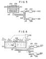
- Figure 6 is a longitudinal cross-sectional view of the soldering apparatus as shown in Figure 5.
- FIG. 1 and 2 of the drawings there is shown a first preferred embodiment of a soldering apparatus comprising a static pool of molten solder 10.
- a nozzle unit 12 is disposed in the pool of molten solder 10 adjacent its bottom and communicates through a pipe 14 with a gas cylinder 16 in which nitrogen gas is contained.
- a valve 18 is disposed in the pipe 14 for controlling a flow rate of the nitrogen gas from the gas cylinder 16 to the nozzle unit 12.
- the nitrogen gas from the cylinder 16 is blown through the nozzle unit 12 into the molten solder to form bubbles 20 which rise rapidly towards the top of the pool of molten solder and finally, burst at the top of the pool.
- printed circuit boards 22 each having electric and/or electronic components including chip type components 24 temporarily bonded thereto in a conventional manner are conveyed along the top of the pool of molten solder 10.
- the rising bubbles 20 in the molten solder are struck against the printed circuit surface of the board 22 to burst at the top of the pool, thereby expelling any flux gases which otherwise would accumulate around terminal portions of the temporarily bonded chip components.
- the chip components are soldered to the printed circuit boards by uniformly contacting with the molten solder.
- the soldering method according to the present invention may be applied to either a high speed jet flow type pool of molten solder or a flow type pool of molten solder to achieve excellent soldering of chip components to a printed circuit board.
- any inert gas other than the nitrogen gas may be used for formation of gas bubbles in the molten solder.
- the use of inert gas is effective to prevent the molten solder from being oxidized by gas to be blown into the molten solder. Thus, wasteful consumption of the molten solder can be prevented.
- the present invention has provided a novel soldering method wherein in soldering to printed circuit board, electric and or electronic components temporarily bonded thereto using a static pool of molten solder, the board and components can be uniformly dipped in the molten solder by striking bubbles against the components to expel any flux gases out of the terminal portions of the components. According to the present invention, any need for formation of conventional vent holes in the printed circuit board can be eliminated and this makes it possible to make a highly concentrated circuit on the board.
- FIG. 1 there is shown a second embodiment of a soldering apparatus comprising a static pool of molten solder 100.
- a container 112 contains liquid 114, such as organic solvent or water which can evaporate at the temperature of molten solder (240°C-270°C).
- a distributor 116 is connected to a supply conduit 118 which is in communication with the interior of the container 112.
- a plurality of nozzle tubes 120 extend from the distributor 116 into the molten solder adjacent the bottom of the pool of molten solder and are provided with nozzles 122 to blow the liquid 114 from the container into the molten solder.
- the container 112 is connected through an inlet conduit 124 to a source (not shown) from which compressed air is applied to the liquid 114 in the container at a predetermined pressure to deliver the liquid through the supply conduit 118 and distributor 116 to the nozzle tubes 120.
- a source not shown
- the liquid 114 is introduced through the nozzles 122 into the molten solder so that it is evaporated in the molten solder with its heat to form bubbles 125 which rapidly rise towards printed circuit boards 126 which are conveyed along the top of the pool of molten solder and have electric and/or electronic components 128 including chip type components temporarily bonded thereto.
- the rising bubbles 125 are struck against the components 128 and the board 126 to bring the molten solder into contact with terminal portions of the components thereby achieving uniform soldering.
- raised portions 130 of molten solder are formed at its top by the rising bubbles so that the molten solder flows in the raised portions 130 in directions as indicated by arrows A and B to expel any gases such as gas from the board and flux .gas which are generated during soldering operation and tend to accumulate around the terminal portions of the components.
- Molecular gas in the form of the bubbles formed by evaporation of the liquid serves to prevent any oxidation of the molten solder so that production of undesirable solder dross is reduced.
- alcohols which become reducing gas in evaporation are suitable to minimize production of solder dross.
- Flux solution which consists of flux dissolved in organic solvent or water may be used as liquid 114 which is introduced into the molten solder for formation of bubbles.
- flux to be required for soldering can be supplied in the form of bubbles through the pool of molten solder onto the printed circuit board and their components so that a fluxer and preheater which has been required heretofore prior to soldering can be omitted.
- the flux solution serves to prevent any oxidation of the molten solder which may take place by formation of bubbles in the molten solder.
- the molten solder is covered at its top with the flux gas to prevent the molten solder from being oxidized by contacting with the atmosphere.
- the liquid may be evaporated during its passage in the nozzle tubes so that it is blown in the form of vapor through the nozzles into the molten solder. This can be achieved by either employing nozzle tubes of any suitable heat- resisting material having a high heat conductivity or controlling flow of the liquid in the nozzle tubes.
- a bubble type pool of molten solder 210 according to a third preferred embodiment of the present invention which comprises a nozzle unit 212 disposed in the pool of molten solder for blowing gases thereinto.
- the nozzle unit 212 is connected to a pipe 214 at its forward end and at the other end, the pipe 214 is connected to an air supply line 216 and an inert gas supply line 218 which are connected to a source of compressed air 220 and a gas cylinder 222 containing inert gas such as nitrogen gas, respectively.
- the air supply line 216 includes a regulator 224 for regulating flow of the compressed air from the source 220 and an electromagnetic valve 226 for controlling supply of the compressed air through the pipe 214 to the nozzle unit 212.
- the inert gas supply line 218 includes a regulator 228 for regulating flow of the inert gas from the cylinder 222 and an electromagnetic valve 230 for controlling supply of the inert gas through the pipe 214 to the nozzle unit 212.
- Printed circuit board 232 having electric and/or electronic components 234 including chip type components temporarily fixed thereto is conveyed along the top of the pool of molten solder 210, following a path as indicated by arrows a, b, c, d and e in Figure 6 of the drawings.
- a device 236 is provided for detecting a position b of the circuit board 232 approaching the top of the molten solder before soldering and a position d of the board 232 leaving from the top of the molten solder after soldering to electrically actuate the electromagnetic valves 226 and 230.
- the electromagnetic valve 226 is opened to supply the compressed air from its source 20 to the nozzle unit 12 whereas the electromagnetic valve 230 is closed.
- the electromagnetic valve 226 is closed whereas the electromagnetic valve 230 is opened to supply the inert gas from its cylinder 222 to the nozzle unit 12.
- the soldering apparatus is operated as follows:
- soldering method wherein in soldering to a printed circuit board, electric and/or electronic components temporarily fixed thereto using a bubble type pool of molten solder, compressed air is introduced into the molten solder during soldering to form air bubbles which rapidly rise in the molten solder toward its top, the rising bubbles are struck against the board and components to solder them to each other, and after soldering, the supply of air is interrupted while inert gas is introduced into the molten solder.
- production of undesirable solder dross can be reduced by blowing air into the molten solder for a short time to be required for soldering.
- any air remaining in the pipe and the nozzle unit after interruption of the supply of air thereto is expelled into the molten solder by introducing the inert gas through the pipe and the nozzle unit into the molten solder to minimize production of undesirable solder dross in the nozzle unit.
Description
- The present invention relates to a soldering method and apparatus, particularly for soldering electric and or electronic components to a printed-circuit board using a pool of molten solder.
- From GB-A-1 352 746 is known a soldering method wherein printed circuit boards are conveyed over a standing solder wave having a flow of inert gas over at least a part of its exposed surface.
- From US―A―4 139 881 is known that electric and/or electronic components such as condensers, resistors, transistors and the like temporarily bonded to a printed-circuit board are soldered to the circuit board by dipping its circuit surface into a static pool of molten solder. In such a soldering system, generation of flux gas and gas from the printed-circuit board itself takes place during soldering operation and the gases tend to accumulate around terminal portions of the components to be soldered. The accumulated gases interfere with uniform soldering of the components to the circuit board. Particularly, soldering of chip type components to the circuit board is significantly affected by accumulation of the flux gas around the components. In order to eliminate this disadvantage, it has been practice that vent holes are formed in the printed circuit board adjacent terminal portions of the chip components to be soldered. The existence of the vent holes results in a restriction of circuits to be formed on the other surface of the board, preventing circuits from being highly concentrated. Moreover, formation of the vent holes in the circuit board results in a high cost and a reduction in strength of the board.
- An attempt has been made to expel the accumulated gases out of the terminal portions of the chip components by means of high speed jet flow of molten solder towards the components. Such a soldering system is successfully applied to relatively thin flat chip components, but still there is a need for formation of vent holes to effect complete expelling of the gases in case that this soldering system is applied to large cylindrical chip components normally called metal electrode facebonding type components and mould type- transistors. Moreover, this soldering system has a disadvantage that because of generation of waves on the top surface of the molten solder, air is involved in the molten solder to oxidize it, thereby forming undesirable solder dross on the top surface of molten solder.
- Accordingly, a main object of the present invention is to provide a novel soldering method and apparatus eliminating disadvantages as described hereinbefore.
- Another object of the present invention is to provide a novel and useful method for soldering to a printed-circuit board, electric and/or electronic components temporarily fixed thereto while preventing flux gases which are generated , in soldering operation from accumulating around terminal portions of the components.
- A still other object of the present invention is to provide a soldering method for soldering to the printed circuit board, electric and/or electronic components temporarily fixed thereto by blowing air or inert gas into the pool of molten solder and by striking bubbles against the board and the components during soldering operation.
- In accordance with the present invention, there is provided a method of the above-mentioned kind comprising conveying printed circuit board having the components temporarily fixed thereto along the top of a pool of molten solder, generating bubbles by blowing gas into the molten solder, the bubbles rapidly rising in the molten solder toward its top, and striking the rising bubbles against the circuit surface to expel any flux gases which otherwise would accumulate around terminal portions of the components and to solder the components to the board.
- In accordance with another embodiment of the present invention, there is provided a soldering method comprising conveying the printed-circuit board having chip components temporarily fixed thereto along the top of a pool of molten solder, supplying into the molten solder liquid under a predetermined pressure to evaporate it with heat of the molten solder, thereby producing vapor bubbles which rapidly rise in the molten solder toward its top, and striking the rising vapor bubbles against the chip components on the printed-circuit board to bring the molten solder into contact with the board and components and to expel any flux gases which otherwise would accumulate around terminal portions of the chip components.
- In accordance with a still other embodiment of the present invention, there is provided a soldering method where during soldering operation, air bubbles are formed in the pool of molten solder by blowing compressed air thereinto and struck against the printed circuit board and the components temporarily fixed thereto which are conveyed along the top of the molten solder to effect soldering of the board and the components to each other and after soldering, inert gas is introduced into the molten solder to minimize its oxidation.
- These and other objects and advantages of the present invention will become apparent from the following description made with reference to the accompanying drawings, in which
- Figure 1 is a transversal cross-sectional view showing a first preferred embodiment of a soldering apparatus suitable to carry out a soldering method according to the present invention;
- Figure 2 is a longitudinal cross-sectional view of the soldering apparatus as shown in Figure 1;
- Figure 3 is a view similar to Figure 1 showing a second preferred embodiment of a soldering apparatus according to the present invention;
- Figure 4 is a longitudinal cross-sectional view of the soldering apparatus as shown in Figure 3;
- Figure 5 is a view similar to Figure 1 showing a third preferred embodiment of a soldering apparatus according to the present invention; and
- Figure 6 is a longitudinal cross-sectional view of the soldering apparatus as shown in Figure 5.
- Referring to Figures 1 and 2 of the drawings, there is shown a first preferred embodiment of a soldering apparatus comprising a static pool of molten solder 10. A
nozzle unit 12 is disposed in the pool of molten solder 10 adjacent its bottom and communicates through apipe 14 with agas cylinder 16 in which nitrogen gas is contained. Avalve 18 is disposed in thepipe 14 for controlling a flow rate of the nitrogen gas from thegas cylinder 16 to thenozzle unit 12. The nitrogen gas from thecylinder 16 is blown through thenozzle unit 12 into the molten solder to formbubbles 20 which rise rapidly towards the top of the pool of molten solder and finally, burst at the top of the pool. - As will be seen in Figure 2, printed
circuit boards 22 each having electric and/or electronic components includingchip type components 24 temporarily bonded thereto in a conventional manner are conveyed along the top of the pool of molten solder 10. During movement of the printedcircuit board 22 along the top of the pool, the risingbubbles 20 in the molten solder are struck against the printed circuit surface of theboard 22 to burst at the top of the pool, thereby expelling any flux gases which otherwise would accumulate around terminal portions of the temporarily bonded chip components. Thus, the chip components are soldered to the printed circuit boards by uniformly contacting with the molten solder. - The soldering method according to the present invention may be applied to either a high speed jet flow type pool of molten solder or a flow type pool of molten solder to achieve excellent soldering of chip components to a printed circuit board.
- Although the preferred embodiment of the present invention has been described hereinbefore in conjunction with the use of nitrogen gas, either air or any inert gas other than the nitrogen gas may be used for formation of gas bubbles in the molten solder. Particularly, the use of inert gas is effective to prevent the molten solder from being oxidized by gas to be blown into the molten solder. Thus, wasteful consumption of the molten solder can be prevented.
- It will be understood from the foregoing that the present invention has provided a novel soldering method wherein in soldering to printed circuit board, electric and or electronic components temporarily bonded thereto using a static pool of molten solder, the board and components can be uniformly dipped in the molten solder by striking bubbles against the components to expel any flux gases out of the terminal portions of the components. According to the present invention, any need for formation of conventional vent holes in the printed circuit board can be eliminated and this makes it possible to make a highly concentrated circuit on the board.
- Referring to Figures 3 and 4 of the drawings, there is shown a second embodiment of a soldering apparatus comprising a static pool of molten solder 100. A
container 112 containsliquid 114, such as organic solvent or water which can evaporate at the temperature of molten solder (240°C-270°C). Adistributor 116 is connected to asupply conduit 118 which is in communication with the interior of thecontainer 112. A plurality ofnozzle tubes 120 extend from thedistributor 116 into the molten solder adjacent the bottom of the pool of molten solder and are provided withnozzles 122 to blow theliquid 114 from the container into the molten solder. Thecontainer 112 is connected through aninlet conduit 124 to a source (not shown) from which compressed air is applied to theliquid 114 in the container at a predetermined pressure to deliver the liquid through thesupply conduit 118 anddistributor 116 to thenozzle tubes 120. Thus, theliquid 114 is introduced through thenozzles 122 into the molten solder so that it is evaporated in the molten solder with its heat to formbubbles 125 which rapidly rise towards printedcircuit boards 126 which are conveyed along the top of the pool of molten solder and have electric and/orelectronic components 128 including chip type components temporarily bonded thereto. The risingbubbles 125 are struck against thecomponents 128 and theboard 126 to bring the molten solder into contact with terminal portions of the components thereby achieving uniform soldering. As will be seen in Figure 4, raisedportions 130 of molten solder are formed at its top by the rising bubbles so that the molten solder flows in the raisedportions 130 in directions as indicated by arrows A and B to expel any gases such as gas from the board and flux .gas which are generated during soldering operation and tend to accumulate around the terminal portions of the components. Molecular gas in the form of the bubbles formed by evaporation of the liquid serves to prevent any oxidation of the molten solder so that production of undesirable solder dross is reduced. Particularly, alcohols which become reducing gas in evaporation are suitable to minimize production of solder dross. - Flux solution which consists of flux dissolved in organic solvent or water may be used as
liquid 114 which is introduced into the molten solder for formation of bubbles. In this case, flux to be required for soldering can be supplied in the form of bubbles through the pool of molten solder onto the printed circuit board and their components so that a fluxer and preheater which has been required heretofore prior to soldering can be omitted. Moreover, the flux solution serves to prevent any oxidation of the molten solder which may take place by formation of bubbles in the molten solder. The molten solder is covered at its top with the flux gas to prevent the molten solder from being oxidized by contacting with the atmosphere. - The liquid may be evaporated during its passage in the nozzle tubes so that it is blown in the form of vapor through the nozzles into the molten solder. This can be achieved by either employing nozzle tubes of any suitable heat- resisting material having a high heat conductivity or controlling flow of the liquid in the nozzle tubes.
- It will be understood from the foregoing that according to the present invention there is provided a novel soldering method wherpin liquid under pressure is introduced into a pool of molten solder to evaporate with heat of the molten solder, thereby forming bubbles which rapidly rises towards a printed circuit board with electric and/or electronic components temporarily fixed thereto, and the rising bubbles are struck against the board and components to bring the molten solder into contact with the board and components. Thus, any flux gas and gas generating from the board which would affect soldering of the components to the printed circuit board can be expelled out of the terminal portions of the components by striking the bubbles against them to achieve excellent soldering. Moreover, according to the present invention, generation of solder dross can be minimized.
- Referring to Figures 5 and 6 of the drawings, there is shown a bubble type pool of
molten solder 210 according to a third preferred embodiment of the present invention which comprises anozzle unit 212 disposed in the pool of molten solder for blowing gases thereinto. Thenozzle unit 212 is connected to apipe 214 at its forward end and at the other end, thepipe 214 is connected to anair supply line 216 and an inertgas supply line 218 which are connected to a source of compressedair 220 and agas cylinder 222 containing inert gas such as nitrogen gas, respectively. Theair supply line 216 includes aregulator 224 for regulating flow of the compressed air from thesource 220 and anelectromagnetic valve 226 for controlling supply of the compressed air through thepipe 214 to thenozzle unit 212. The inertgas supply line 218 includes aregulator 228 for regulating flow of the inert gas from thecylinder 222 and anelectromagnetic valve 230 for controlling supply of the inert gas through thepipe 214 to thenozzle unit 212. - Printed
circuit board 232 having electric and/orelectronic components 234 including chip type components temporarily fixed thereto is conveyed along the top of the pool ofmolten solder 210, following a path as indicated by arrows a, b, c, d and e in Figure 6 of the drawings. - A
device 236 is provided for detecting a position b of thecircuit board 232 approaching the top of the molten solder before soldering and a position d of theboard 232 leaving from the top of the molten solder after soldering to electrically actuate theelectromagnetic valves device 236 electrically senses theboard 232 at the position b, theelectromagnetic valve 226 is opened to supply the compressed air from itssource 20 to thenozzle unit 12 whereas theelectromagnetic valve 230 is closed. When thedevice 236 senses theboard 232 at its position d, theelectromagnetic valve 226 is closed whereas theelectromagnetic valve 230 is opened to supply the inert gas from itscylinder 222 to thenozzle unit 12. - The soldering apparatus is operated as follows:
- As the printed
circuit board 232 is conveyed from its position a to the approaching position b, detectingdevice 236 electrically senses theboard 232 at position b to actuate theelectromagnetic valve 226 from is closed position to an open position while keeping theelectromagnetic valve 230 closed. Then, compressed air from theair supply line 216 andpipe 214 is blown through thenozzle unit 212 into the molten solder to form air bubbles 238 which rapidly rise toward the top of the molten solder. The rising air bubbles are struck against the printedcircuit board 232 with thechip components 234 temporarily bonded thereto, which is conveyed from the approaching position b to a soldering position c where thechip components 234 are uniformly soldered to thecircuit board 232 under the action of the rising air bubbles 238 without spreading out any molten solder through apertures (not shown) in the board. After soldering, theboard 232 is conveyed from the soldering position c to the leaving position d where the detectingdevice 236 electrically senses existence of theboard 232 to close thevalve 226 for interruption of the supply of air and to open thevalve 230 for introduction of inert gas from itscylinder 222 through thegas supply line 218,pipe 214 andnozzle unit 212 into the molten solder. The introduction of the inert gas into the molten solder causes any air remaining in thepipe 214 to expel out of thepipe 214 and thenozzle unit 212, thereby preventing the molten solder from being oxidized in thenozzle unit 212 and removing any solder dross accumulated on thenozzle unit 212. When the inert gas has been introduced through thenozzle unit 212 into the molten solder a predetermined time, thevalve 230 is closed for interruption of the supply of the inert gas by actuating it through a timer (not shown) in the detectingdevice 236. Alternatively, introduction of the inert gas into the molten solder may be continued until air begins to be blown into the molten solder for soldering. Although in the preferred embodiment as shown in the drawings, it has been described that the inert gas is introduced into the molten solder when the board is in the leaving position d, the introduction of the inert gas may be begun immediately after the soldering has been completed. - It will be understood from the foregoing that there has been provided a soldering method wherein in soldering to a printed circuit board, electric and/or electronic components temporarily fixed thereto using a bubble type pool of molten solder, compressed air is introduced into the molten solder during soldering to form air bubbles which rapidly rise in the molten solder toward its top, the rising bubbles are struck against the board and components to solder them to each other, and after soldering, the supply of air is interrupted while inert gas is introduced into the molten solder. According to the present invention, production of undesirable solder dross can be reduced by blowing air into the molten solder for a short time to be required for soldering. Moreover, any air remaining in the pipe and the nozzle unit after interruption of the supply of air thereto is expelled into the molten solder by introducing the inert gas through the pipe and the nozzle unit into the molten solder to minimize production of undesirable solder dross in the nozzle unit.
Claims (11)
Applications Claiming Priority (6)
| Application Number | Priority Date | Filing Date | Title |
|---|---|---|---|
| JP105107/80 | 1980-08-01 | ||
| JP10510780A JPS5731195A (en) | 1980-08-01 | 1980-08-01 | Method of soldering leadless electric part |
| JP53381 | 1981-01-08 | ||
| JP533/81U | 1981-01-08 | ||
| JP56053040A JPS57169295A (en) | 1981-04-10 | 1981-04-10 | Method of soldering electric part or like |
| JP53040/81 | 1981-04-10 |
Publications (2)
| Publication Number | Publication Date |
|---|---|
| EP0045909A1 EP0045909A1 (en) | 1982-02-17 |
| EP0045909B1 true EP0045909B1 (en) | 1985-04-24 |
Family
ID=27274501
Family Applications (1)
| Application Number | Title | Priority Date | Filing Date |
|---|---|---|---|
| EP81106012A Expired EP0045909B1 (en) | 1980-08-01 | 1981-07-30 | A soldering method and apparatus |
Country Status (4)
| Country | Link |
|---|---|
| EP (1) | EP0045909B1 (en) |
| CA (1) | CA1159575A (en) |
| DE (1) | DE3170125D1 (en) |
| GB (1) | GB2083773B (en) |
Families Citing this family (6)
| Publication number | Priority date | Publication date | Assignee | Title |
|---|---|---|---|---|
| DE3111809C2 (en) * | 1981-03-25 | 1985-05-15 | Zevatron GmbH Gesellschaft für Fertigungseinrichtungen der Elektronik, 3548 Arolsen | Method and device for machine soldering of workpieces |
| GB2117690B (en) * | 1982-04-02 | 1986-01-08 | Zevatron Gmbh | Apparatus for soldering workpieces |
| DE4402758A1 (en) * | 1994-01-31 | 1995-08-03 | Moedinger Volker | Method for applying fluxing agent to PCBs |
| US5509598A (en) * | 1994-05-31 | 1996-04-23 | The Boc Group, Inc. | Wave soldering apparatus and process |
| DE19955659A1 (en) * | 1999-11-19 | 2001-05-31 | Messer Griesheim Gmbh | Flux medium-free solder device with reactive gas enriched metal melting for electronic components, has solder container for molten solder material, and gas delivery device for introducing reducing reactive gas |
| CN109392299B (en) * | 2017-08-08 | 2022-03-29 | 伊利诺斯工具制品有限公司 | Solder paste nozzle, workbench and solder paste adding device |
Citations (1)
| Publication number | Priority date | Publication date | Assignee | Title |
|---|---|---|---|---|
| US4139881A (en) * | 1976-12-17 | 1979-02-13 | Matsushita Electric Industrial Co., Ltd. | Circuit board assembly and method of manufacturing the same |
Family Cites Families (2)
| Publication number | Priority date | Publication date | Assignee | Title |
|---|---|---|---|---|
| US3705457A (en) * | 1970-11-02 | 1972-12-12 | Electrovert Mfg Co Ltd | Wave soldering using inert gas to protect pretinned and soldered surfaces of relatively flat workpieces |
| US4093113A (en) * | 1977-02-08 | 1978-06-06 | Usm Corporation | Seam soldering mechanism |
-
1981
- 1981-07-28 GB GB8123286A patent/GB2083773B/en not_active Expired
- 1981-07-30 DE DE8181106012T patent/DE3170125D1/en not_active Expired
- 1981-07-30 EP EP81106012A patent/EP0045909B1/en not_active Expired
- 1981-07-31 CA CA000383012A patent/CA1159575A/en not_active Expired
Patent Citations (1)
| Publication number | Priority date | Publication date | Assignee | Title |
|---|---|---|---|---|
| US4139881A (en) * | 1976-12-17 | 1979-02-13 | Matsushita Electric Industrial Co., Ltd. | Circuit board assembly and method of manufacturing the same |
Also Published As
| Publication number | Publication date |
|---|---|
| CA1159575A (en) | 1983-12-27 |
| GB2083773A (en) | 1982-03-31 |
| GB2083773B (en) | 1984-10-24 |
| EP0045909A1 (en) | 1982-02-17 |
| DE3170125D1 (en) | 1985-05-30 |
Similar Documents
| Publication | Publication Date | Title |
|---|---|---|
| US3865298A (en) | Solder leveling | |
| US4401253A (en) | Mass soldering system | |
| EP0045909B1 (en) | A soldering method and apparatus | |
| US4995411A (en) | Mass soldering system providing an improved fluid blast | |
| WO2008030272A2 (en) | System, apparatus and methods for board cooling | |
| US3924794A (en) | Solder leveling process | |
| GB1602779A (en) | Methods and apparatus for mass soldering of printed circuit boards | |
| JP2003078242A (en) | Method of partially soldering printed board | |
| US4375271A (en) | Soldering method for electric and or electronic component | |
| JP2004106061A (en) | Manufacturing method for printed circuit board unit and soldering device | |
| US4433805A (en) | Soldering method for electric and or electronic components | |
| JP3933879B2 (en) | Method for preventing oxidation of molten solder in water vapor atmosphere | |
| CA1091102A (en) | Mass wave soldering system | |
| JPH02307671A (en) | Soldering method | |
| JPH0661638A (en) | Method and machine for soldering printed board | |
| JP2000332401A (en) | Method of cooling soldered product, soldered product cooling apparatus and soldering apparatus | |
| JP2002368404A (en) | Partial soldering method of printed board and partial jet solder bath | |
| JP2003304037A (en) | Method for manufacturing printed board and printed board unit | |
| JP2004186425A (en) | Soldering apparatus and soldering method | |
| JPH0677624A (en) | Method and system for etching printed wiring board | |
| JPS5884673A (en) | Soldering method | |
| JPH04257293A (en) | Method and apparatus for dip soldering | |
| JPS57190767A (en) | Soldering method for chip parts | |
| JPH01162566A (en) | Foaming flux coating device | |
| JP2001352162A (en) | Soldering device |
Legal Events
| Date | Code | Title | Description |
|---|---|---|---|
| PUAI | Public reference made under article 153(3) epc to a published international application that has entered the european phase |
Free format text: ORIGINAL CODE: 0009012 |
|
| AK | Designated contracting states |
Designated state(s): BE CH DE FR NL |
|
| 17P | Request for examination filed |
Effective date: 19820504 |
|
| GRAA | (expected) grant |
Free format text: ORIGINAL CODE: 0009210 |
|
| AK | Designated contracting states |
Designated state(s): BE CH DE FR LI NL |
|
| REF | Corresponds to: |
Ref document number: 3170125 Country of ref document: DE Date of ref document: 19850530 |
|
| ET | Fr: translation filed | ||
| PLBE | No opposition filed within time limit |
Free format text: ORIGINAL CODE: 0009261 |
|
| STAA | Information on the status of an ep patent application or granted ep patent |
Free format text: STATUS: NO OPPOSITION FILED WITHIN TIME LIMIT |
|
| 26N | No opposition filed | ||
| PGFP | Annual fee paid to national office [announced via postgrant information from national office to epo] |
Ref country code: DE Payment date: 20000523 Year of fee payment: 20 |
|
| PGFP | Annual fee paid to national office [announced via postgrant information from national office to epo] |
Ref country code: FR Payment date: 20000524 Year of fee payment: 20 |
|
| PGFP | Annual fee paid to national office [announced via postgrant information from national office to epo] |
Ref country code: BE Payment date: 20000608 Year of fee payment: 20 |
|
| PGFP | Annual fee paid to national office [announced via postgrant information from national office to epo] |
Ref country code: NL Payment date: 20000731 Year of fee payment: 20 |
|
| PGFP | Annual fee paid to national office [announced via postgrant information from national office to epo] |
Ref country code: CH Payment date: 20001004 Year of fee payment: 20 |
|
| BE20 | Be: patent expired |
Free format text: 20010730 *AIWA CO. LTD. |
|
| PG25 | Lapsed in a contracting state [announced via postgrant information from national office to epo] |
Ref country code: LI Free format text: LAPSE BECAUSE OF EXPIRATION OF PROTECTION Effective date: 20010729 Ref country code: CH Free format text: LAPSE BECAUSE OF EXPIRATION OF PROTECTION Effective date: 20010729 |
|
| PG25 | Lapsed in a contracting state [announced via postgrant information from national office to epo] |
Ref country code: NL Free format text: LAPSE BECAUSE OF EXPIRATION OF PROTECTION Effective date: 20010730 |
|
| REG | Reference to a national code |
Ref country code: CH Ref legal event code: PL |
|
| NLV7 | Nl: ceased due to reaching the maximum lifetime of a patent |
Effective date: 20010730 |