EP0045610B1 - A semiconductor read only memory device - Google Patents
A semiconductor read only memory device Download PDFInfo
- Publication number
- EP0045610B1 EP0045610B1 EP81303429A EP81303429A EP0045610B1 EP 0045610 B1 EP0045610 B1 EP 0045610B1 EP 81303429 A EP81303429 A EP 81303429A EP 81303429 A EP81303429 A EP 81303429A EP 0045610 B1 EP0045610 B1 EP 0045610B1
- Authority
- EP
- European Patent Office
- Prior art keywords
- transistor
- gate
- transistors
- level
- memory device
- Prior art date
- Legal status (The legal status is an assumption and is not a legal conclusion. Google has not performed a legal analysis and makes no representation as to the accuracy of the status listed.)
- Expired
Links
Images


Classifications
-
- G—PHYSICS
- G11—INFORMATION STORAGE
- G11C—STATIC STORES
- G11C17/00—Read-only memories programmable only once; Semi-permanent stores, e.g. manually-replaceable information cards
- G11C17/14—Read-only memories programmable only once; Semi-permanent stores, e.g. manually-replaceable information cards in which contents are determined by selectively establishing, breaking or modifying connecting links by permanently altering the state of coupling elements, e.g. PROM
- G11C17/18—Auxiliary circuits, e.g. for writing into memory
-
- G—PHYSICS
- G11—INFORMATION STORAGE
- G11C—STATIC STORES
- G11C17/00—Read-only memories programmable only once; Semi-permanent stores, e.g. manually-replaceable information cards
- G11C17/08—Read-only memories programmable only once; Semi-permanent stores, e.g. manually-replaceable information cards using semiconductor devices, e.g. bipolar elements
- G11C17/10—Read-only memories programmable only once; Semi-permanent stores, e.g. manually-replaceable information cards using semiconductor devices, e.g. bipolar elements in which contents are determined during manufacturing by a predetermined arrangement of coupling elements, e.g. mask-programmable ROM
- G11C17/12—Read-only memories programmable only once; Semi-permanent stores, e.g. manually-replaceable information cards using semiconductor devices, e.g. bipolar elements in which contents are determined during manufacturing by a predetermined arrangement of coupling elements, e.g. mask-programmable ROM using field-effect devices
Definitions
- This invention relates to a semiconductor memory device, especially to a semiconductor mask read only memory device with a high speed read cycle.
- ROM read only memory
- PROM programmable read only memory
- a mask ROM used for storing a computer program etc. on a larger scale and to speed up its read out time.
- Fig. 1 a semiconductor mask ROM is illustrated.
- the ROM of Fig. 1 is not part of the prior art.
- the circuit of Fig. 1 is a development of a prior art circuit (e.g. US-A-3765002) which, in particular, lacks the gate transistor Q G of Fig. 1.
- the gate of the gate transistor Q G is supplied with the output signal of a voltage control circuit CNT.
- a depletion type transistor O c1 , and transistors Q c2 and Q c3 are connected in series between the voltage source V cc and the ground.
- the voltage V(N o ) at the node No where the load transistor Q L and the gate transistor Q G are connected, is supplied to the data bus line DB through the buffer circuit BUF as shown.
- the buffer circuit BUF there are provided gate circuits GT 1 , GT 2 and transistors Q B1 , Q B2 interconnected as shown in Fig. 1.
- the gate of the transistor Q ij is connected to the word line WL, and its source is connected to the ground.
- the drain of the transistor Q ij is connected to the bit line BL j in the case that the data "0" is stored in the memory cell of the transistor Q, j , and the drain of the transistor Q ij is disconnected to the bit line BL j in the case that the data "1" is stored in this memory cell.
- the read operation in the ROM of Fig. 1 will be described as follows.
- the ROM of Fig. 1 has two operation modes, one mode is of the preparation operation for reading and other mode is of the reading operation.
- the preparation operation for reading all selecting signals A o , A 1 ...A n of the multiplexer MPX and all word lines WL 0 , WL 1 ...WL m are rendered to the "H" level.
- one of the selecting signals A o , A 1 ...A n and one of the word lines WL o , WL 1 ...WL m are kept at the "H” level, and the other selecting signals and the other word lines are turned to the "L” level.
- the selecting signals A 1 and the word line WL 0 are kept at the "H” level, and the other selecting signals Ao, A 2 ...A n and the other word lines WL 1 , WL2...WLm are turned to the "L" level.
- the transistor Q x is conductive and all the other transistors Q xj of the multiplexer MPX are non-conductive.
- the transistors Q i1 of bit line BL 1 only the transistor Q ol is conductive and the other transistors Q j1 are non-conductive.
- the transistor Q 01 is connected to the bit line BL 1 , the current suplied from the voltage source V cc flows through transistors Q L , Q G , Q x1 and Q 01 , to the ground, and therefore the charge is not accumulated in the stray capacity of the node No and the potential at the node No is held at the "L" level. Accordingly, the data of "L" level (that is "0") is transmitted to the data bus line DB through the buffer circuit BUF.
- the size of the transistor Q lj of the memory cell becomes smaller, so that the resistance of the main current path of the transistor Q ij becomes greater. Since the output signal level of the node No in the case of reading "L" level data, is mainly determined by the ratio between the resistors of the memory cell transistor Q ij and the load transistor Q,, in order to obtain an appropriate output signal level, it is necessary to make the resistance of the load transitor Q L greater proportionally.
- the gate transistor Q G is provided.
- the function of the gate transistor Q G in the above-mentioned reading operation of the memory cell transistor Q 11 will now be described.
- the charge accumulated in the stray capacity of the bit line BL 1 is supplied from the voltage source V cc through the load transistor Q L , the gate transistor Q G and the transistor Q x1 of the muliplexer MPX.
- the output signal V INT of the gate voltage control circuit CNT is applied to the gate of the gate transitor Q G , and if the potential at the node N 1 connected to the source of the gate transistor Q G is lower than the level of the signal V 1NT , the resistance of the main current path of the gate transistor Q G is relatively small, and therefore the potential at the bit line BL 1 rises gradually according to the drive capacity of the load transistor Q L .
- the potentials at the nodes No and N 1 also rise, and when the difference between the potentials at the gate of the gate transistor Q G and at the node N 1 is below the threshold voltage V TH of the gate transistor Q G , the gate transistor Q G is turned into the cut-off state so that the bit line BL 1 and the node N 1 is separated from the node No. Therefore, the potential at the node No which has been rising gradually in accordance with the potential at the bit line BL, then rises rapidly and turns to the "H" level.
- the main object of the present invention is to solve the above-mentioned problems of semiconductor read only memory devices and to speed up the read cycle time in the memory device with a larger memory capacity and with integration on a larger scale.
- a semiconductor read only memory device comprising a plurality of bit lines, a plurality of word lines, a load transistor electrically connected to a voltage source, a multiplexer including a plurality of transistors each of which is electrically connected to one of said plurality of bit lines, and a memory cell array in which each memory cell has one transistor having a gate electrically connected to one of said word lines and a source or a drain region electrically connected to one of said bit lines, characterised by a gate transistor, and a gate voltage control circuit for selectively providing, to the gate of said gate transistor, a higher level signal during a preparation period of said memory device and lower level signal during a reading period of said memory device.
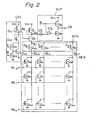
- FIG. 2 A semiconductor read only memory device in accordance with the present invention is illustrated in Fig. 2.
- the device shown in Fig. 2 has the same construction as that of the device of Fig. 1 except the gate voltage control circuit CNT.
- the gate voltage control circuit CNT has a depletion type transistor Q c1 and transistors Q c2 , Q c3 , Q c4 and Q c5 .
- the ROM of Fig. 2 may be supplied with a clock pulse signal P and its inverted signal P from a clock pulse generating circuit such as is shown in Fig. 3.
- a clock pulse generating circuit of Fig. 3 a waveform generated by a quartz oscillator QAZ and an inverting amplifier IV 1 is shaped by a wave-shaping circuit WSP and then the shaped waveform is outputted as a system clock pulse P and its inverted waveform is outputted as P.
- the wave-shaping circuit several inverters IV 2 , IV 3 ...IV 5 are connected in series.
- Figs. 4 (1) through (6) there are illustrated various waveforms to explain the access operation of the ROM of Fig. 2.
- the system clock pulse P and its inverted pulse P are illustrated respectively.
- the waveform P illustrated in Fig. 4 (1) the period when the level of the waveform is "L" is the preparation period T PREP of the memory device, and the period when the level of the waveform is "H” in the reading period TREAD of the memory device. Accordingly, in the ROM of Fig. 2, the read operation is effected in phase with the system clock P.
- the system clock signal P is applied to the gate of the transistor Q c4
- the inverted signal P of the system clock is applied to the gate of the transistor Q c5 . Therefore, in the preparation period Tp RE p, the transistor Q c4 of OFF and the transistor Q c5 is ON and consequently the gate voltage of the transistor Q c3 is the "L" level and the transistor Q c3 is OFF. Accordingly, the voltage at the node N 2 connected to the gate of the gate transistor Q G becomes almost equal to the voltage source V cc , because the node N 2 is connected to V cc through the depletion type transistor Q c1 and cut-off from the ground.
- the transistor Q c4 is ON and the transistor Q c5 is OFF, and then the transistor Q ce in ON. Accordingly, the current path between the voltage source V cc and the ground is formed through the transistors Q c1 , Q c2 and Q c3 , and the voltage at the node N 2 applied to the gate of the gate transistor Q G is dropped to the intermediate level V INT which is divided by the depletion type transistor Q c1 , and other transistors Q c2 , Q c3'
- Figs. 4 (3) through (6) there are illustrated voltage waveforms at various points of the ROM of Fig. 2 in the case that the memory cell transistor Q 11 is read-out in the first reading period TREAD (between T, and T 2 ) in Fig. 4 (1), and the memory cell transistor Q 01 , is read-out in the second reading period TREAD (between T 3 and T4).
- bit line BL 1 Since the memory cell transistor Q 11 which corresponds to the bit line BL, and the word line WL, is not connected to the bit line BL 1 the bit line BL 1 is separated from the ground and consequently the potentials at the bit line BL 1 and the node N 1 begin to rise because of the current supplied through the load transistor Q L and the gate transistor Q G .
- the potentials V(N 1 ) and V(N o ) at the nodes N 1 and N 2 are illustrated respectively.
- the intermediate level signal VINT is applied to the gate of the gate transistor Q G in the reading period T READ , and the potential V(N 1 ) is almost the ground level at first so that the potential V(N 1 ) at the node N 1 rises gradually by means of the relatively great resistance of the load transistor Q L
- the gate transistor Q G turns OFF and after that time the potential V(N 1 ) does not rise any more.
- the potential V(N o ) at the node No begins to rise up rapidly because the node No is separated from the node N 1 and the bit line BL 1 , and the potential V(N o ) attains the "H" level immediately.
- the read operation of the "H" level data is made shorter than that in the case where the gate transistor Q G does not turn off as shown in the broken line of Fig. 4 (6).
- the system clock signal P turns to the "L" level, and then all the selecting signals A o , A 1 ...A n and all the word lines WL 0 , WL 1 ...WL m turn to the "H" level. Consequently, all the transistors Q xo , Q x1 ...Q xn of the multiplexer MPX turn ON and all the memory cell transistors Q ij also turn ON. Then, the potentials at the bit line BL 1 and the node N 1 decrease rapidly to the ground potential. On the other hand, the charge accumulated in the stray capacity of the node No is drawn to the node N 1 through the gate transistor Q G .
- the V cc level signal is applied to the gate of the gate transistor Q G in the preparation time Tp RE p so that the gate transistor Q G is sufficiently conductive and its resistance is substantially small. Therefore, the potential V(N o ) at the node No drops to the "L" level in a short time.
- the system clock signal P turns to the "H" level, and all the selecting signals A o , A 2 ...A n except A 1 and all the word lines WL 1 , WL2...WLm except WL 0 turn to the "L" level. Accordingly, only the transistor Q x1 of the multiplexer MPX is kept ON and other transistors Q xo , Q x2 ...Q xn turn OFF. Therefore, only the bit line BL 1 is connected to the node N 1 .
- the memory cell transistor Q 01 Since the memory cell transistor Q 01 , is turned ON by the word line WL 1 and the transistor Q 01 is connected to the bit line BL 1 , the potential atthe bit line BL 1 is kept at the "L” level, and the potentials at the nodes N 1 and No are also kept at the "L” level. Thus, the reading operation of the "L" level data is effected almost instantly.
- the read operation time can be made shorter.
Landscapes
- Read Only Memory (AREA)
Description
- This invention relates to a semiconductor memory device, especially to a semiconductor mask read only memory device with a high speed read cycle.
- Generally, there are two types of read only memory (ROM) which may be used for the storage device of a digital computer, one is a programmable read only memory (PROM) which can be programmed when it is used, the other is a mask ROM which is programmed during the manufacturing process.
- In recent years, in accordance with the miniaturizing and the speed up of the computer, it is required to integrate a mask ROM used for storing a computer program etc. on a larger scale and to speed up its read out time. In Fig. 1, a semiconductor mask ROM is illustrated. The mask ROM of Fig. 1 comprises a load transistor of a depletion type QL, a multiplexer MPX consisting of a plurality of transistors Qxo, Ox1...Qxn to the gates of which the address selecting signals Ao, A1...An are respectively applied, a memory cell array having transistors Qij (i=0, 1...m, j=0, 1...n) with gates connected to the word lines WL0, WL1...WLm, and a gate transistor QG inserted between the load transistor QL and the multiplexer MPX. The ROM of Fig. 1 is not part of the prior art. The circuit of Fig. 1 is a development of a prior art circuit (e.g. US-A-3765002) which, in particular, lacks the gate transistor QG of Fig. 1.
- As shown in Fig. 1, the gate of the gate transistor QG is supplied with the output signal of a voltage control circuit CNT. In the voltage control circuit CNT, a depletion type transistor Oc1, and transistors Qc2 and Qc3 are connected in series between the voltage source Vcc and the ground. The voltage V(No) at the node No where the load transistor QL and the gate transistor QG are connected, is supplied to the data bus line DB through the buffer circuit BUF as shown. In the buffer circuit BUF, there are provided gate circuits GT1, GT2 and transistors QB1, QB2 interconnected as shown in Fig. 1.
- The transistors Ox0, Ox1...Qxn of the multiplexer MPX, are connected to the bit lines BL0, BL1...BLn respectively, the transistor Qij (i=0, 1...m, j=0, 1...n) of the memory cell array is corresponding to the word line WL, and the bit line BLj. The gate of the transistor Qij is connected to the word line WL, and its source is connected to the ground. The drain of the transistor Qij is connected to the bit line BLj in the case that the data "0" is stored in the memory cell of the transistor Q,j, and the drain of the transistor Qij is disconnected to the bit line BLj in the case that the data "1" is stored in this memory cell.
- The read operation in the ROM of Fig. 1 will be described as follows. The ROM of Fig. 1 has two operation modes, one mode is of the preparation operation for reading and other mode is of the reading operation. In the preparation operation for reading all selecting signals Ao, A1...An of the multiplexer MPX and all word lines WL0, WL1...WLm are rendered to the "H" level. Therefore, all transistors Qij of the memory cell array MCA become conductive and consequently the charge accumulated in the stray capacity of each bit line BLo, BL1...BLn is discharged through the transistors Qij connected to the bit line BLj and the potentials at the bit lines BL0, BLI... BLn decrease to the ground level. According to the decrease of the potentials at the bit lines BL0, BL1...BLn, the charge accumulated in the stray capacity of the node No is discharged through the gate transistor QG and the transistors Qx0, Qx1...Qxn of the multiplexer MPX. Therefore, the potential at the node No turns to the "L" level.
- Then, in the reading operation, in order to read the data stored in a certain memory cell, one of the selecting signals Ao, A1...An and one of the word lines WLo, WL1...WLm are kept at the "H" level, and the other selecting signals and the other word lines are turned to the "L" level. For example, in the case of reading the memory cell of the transistor Q01, only the selecting signals A1 and the word line WL0 are kept at the "H" level, and the other selecting signals Ao, A2...An and the other word lines WL1, WL2...WLm are turned to the "L" level. In this case, only the transistor Qx, is conductive and all the other transistors Qxj of the multiplexer MPX are non-conductive. Among the transistors Qi1 of bit line BL1, only the transistor Qol is conductive and the other transistors Qj1 are non-conductive. As the transistor Q01 is connected to the bit line BL1, the current suplied from the voltage source Vcc flows through transistors QL, QG, Qx1 and Q01, to the ground, and therefore the charge is not accumulated in the stray capacity of the node No and the potential at the node No is held at the "L" level. Accordingly, the data of "L" level (that is "0") is transmitted to the data bus line DB through the buffer circuit BUF.
- Then, in the case of reading the memory cell of the transistor Q11, only the selecting signal A1 and the word line WL1 are held to be the "H" level. Accordingly, among the transistors of the multiplexer MPX only Qx1 is conductive and among the transistors of the bit line BL1 only Q11 is conductive. In this case, the transistor Q11 is disconnected to the bit line BL1 so that the bit line BL1 is disconnected to the ground. Therefore, the current supplied from the voltage source Vcc is flowing into the stray capacity of the bit line BL1 through transistors QL, QG and Qx1, and the capacity is charged by this current. Thus, the potentials at the bit line BL1 and the node No rise up and reach to the "H" level. This "H" level signal of the node No is transmitted to the data bus DB through the buffer circuit BUF.
- However, in the ROM of Fig. 1, together with the increase of the memory capacity and the integration scale of a memory device, the size of the transistor Qlj of the memory cell becomes smaller, so that the resistance of the main current path of the transistor Qij becomes greater. Since the output signal level of the node No in the case of reading "L" level data, is mainly determined by the ratio between the resistors of the memory cell transistor Qij and the load transistor Q,, in order to obtain an appropriate output signal level, it is necessary to make the resistance of the load transitor QL greater proportionally. However, since in accordance with the increase in the resistance of the main current path of the load transistor QL, the drive capacity of the load transistor QL decreases, it takes a considerably longer time to charge the bit lines having an equivalently large capacity, and to raise the potential to the "H" level. In the prior art circuit lacking QG this results in an increase in access time.
- In order to prevent an increase in the access time of the memory device according to the above-mentioned decrease of the drive capacity of the load transistor QL, in accordance with the ROM of Fig. 1 the gate transistor QG is provided. The function of the gate transistor QG in the above-mentioned reading operation of the memory cell transistor Q11 will now be described. As described above, in the reading operation of the transistor Q11, the charge accumulated in the stray capacity of the bit line BL1 is supplied from the voltage source Vcc through the load transistor QL, the gate transistor QG and the transistor Qx1 of the muliplexer MPX. The output signal VINT of the gate voltage control circuit CNT is applied to the gate of the gate transitor QG, and if the potential at the node N1 connected to the source of the gate transistor QG is lower than the level of the signal V1NT, the resistance of the main current path of the gate transistor QG is relatively small, and therefore the potential at the bit line BL1 rises gradually according to the drive capacity of the load transistor QL. In accordance with this, the potentials at the nodes No and N1 also rise, and when the difference between the potentials at the gate of the gate transistor QG and at the node N1 is below the threshold voltage VTH of the gate transistor QG, the gate transistor QG is turned into the cut-off state so that the bit line BL1 and the node N1 is separated from the node No. Therefore, the potential at the node No which has been rising gradually in accordance with the potential at the bit line BL,, then rises rapidly and turns to the "H" level.
- As described above, in accordance with the ROM of Fig. 1, since the stray capacity of the bit line BLj is separated from the node No by means of the gate transistor QG, in spite of the small drive capacity of the load transistor QL, an increase in the access time of the memory cell can be prevented. However, since the gate voltage of the gate transistor QG is intermediate between the voltage source Vcc and the ground level, the resistance value of the gate transistor QG as a resistance element is considerably great. Therefore, in the ROM of Fig. 1, though the reading operation time becomes shorter, there is a problem that it takes a rather long time to decrease the potential at the node No to the "L" level in the preparation operation for reading.
- The main object of the present invention is to solve the above-mentioned problems of semiconductor read only memory devices and to speed up the read cycle time in the memory device with a larger memory capacity and with integration on a larger scale.
- In accordance with the present invention, there is provided a semiconductor read only memory device comprising a plurality of bit lines, a plurality of word lines, a load transistor electrically connected to a voltage source, a multiplexer including a plurality of transistors each of which is electrically connected to one of said plurality of bit lines, and a memory cell array in which each memory cell has one transistor having a gate electrically connected to one of said word lines and a source or a drain region electrically connected to one of said bit lines, characterised by a gate transistor, and a gate voltage control circuit for selectively providing, to the gate of said gate transistor, a higher level signal during a preparation period of said memory device and lower level signal during a reading period of said memory device.
-
- Fig. 1 illustrates a circuit diagram of a semiconductor read only memory device which is not part of the prior art,
- Fig. 2 illustrates a circuit diagram of a semiconductor read only memory device in accordance with the present invention,
- Fig. 3 illustrates a circuit diagram of a clock pulse generator supplying the ROM of Fig. 2 with a system clock pulse, and
- Figs. 4 (1) through (6) illustrate various waveforms for explaining the read operation of the ROM of Fig. 2.
- A semiconductor read only memory device in accordance with the present invention is illustrated in Fig. 2. In the read only memory of Fig. 2, there are provided a load transistor QL, a multiplexer MPX including a plurality of transistors Qxo, Qx1...Qxn, a memory cell array MCA consisting of transistors Qij(i=0, 1...m, j=O, 1...n), a gate transistor QG inserted between the load transistor QL and the multiplexer MPX, a gate voltage control circuit CNT controlling the gate voltage of the gate transistor QG, and, a buffer circuit BUF transmitting the voltage level at the node No between the load transistor QL and the gate transistor QG to the data bus line DB.
- The device shown in Fig. 2 has the same construction as that of the device of Fig. 1 except the gate voltage control circuit CNT. The gate voltage control circuit CNT has a depletion type transistor Qc1 and transistors Qc2, Qc3, Qc4 and Qc5.
- The ROM of Fig. 2 may be supplied with a clock pulse signal P and its inverted signal P from a clock pulse generating circuit such as is shown in Fig. 3. In the clock pulse generating circuit of Fig. 3, a waveform generated by a quartz oscillator QAZ and an inverting amplifier IV1 is shaped by a wave-shaping circuit WSP and then the shaped waveform is outputted as a system clock pulse P and its inverted waveform is outputted as P. In the wave-shaping circuit, several inverters IV2, IV3...IV5 are connected in series.
- In Figs. 4 (1) through (6) , there are illustrated various waveforms to explain the access operation of the ROM of Fig. 2. In Figs. 4 (1) and (2) , the system clock pulse P and its inverted pulse P are illustrated respectively. In the waveform P illustrated in Fig. 4 (1), the period when the level of the waveform is "L" is the preparation period TPREP of the memory device, and the period when the level of the waveform is "H" in the reading period TREAD of the memory device. Accordingly, in the ROM of Fig. 2, the read operation is effected in phase with the system clock P.
- In the control circuit CNT of Fig. 2, the system clock signal P is applied to the gate of the transistor Qc4, and the inverted signal P of the system clock is applied to the gate of the transistor Qc5. Therefore, in the preparation period TpREp, the transistor Qc4 of OFF and the transistor Qc5 is ON and consequently the gate voltage of the transistor Qc3 is the "L" level and the transistor Qc3 is OFF. Accordingly, the voltage at the node N2 connected to the gate of the gate transistor QG becomes almost equal to the voltage source Vcc, because the node N2 is connected to Vcc through the depletion type transistor Qc1 and cut-off from the ground. On the other hand, in the reading period TREAD, since the transistor Qc4 is ON and the transistor Qc5 is OFF, and then the transistor Qce in ON. Accordingly, the current path between the voltage source Vcc and the ground is formed through the transistors Qc1, Qc2 and Qc3, and the voltage at the node N2 applied to the gate of the gate transistor QG is dropped to the intermediate level VINT which is divided by the depletion type transistor Qc1, and other transistors Qc2, Qc3'
- In Figs. 4 (3) through (6), there are illustrated voltage waveforms at various points of the ROM of Fig. 2 in the case that the memory cell transistor Q11 is read-out in the first reading period TREAD (between T, and T2) in Fig. 4 (1), and the memory cell transistor Q01, is read-out in the second reading period TREAD (between T3 and T4).
- As shown in Figs. 4 (3) and (4), in the preparation period TPREP, all the selecting signals Ao, A1...An for the transistors Ox0, Qx1...Qxn, are "H" level and all the word lines WL0, WL1...WLm are also "H" level. Therefore, the potential V(N1) at the node N1 and the potential V(No) at the node No are "L" level. At the instant T1, the system clock signal P rises up to "H" level and then all the selecting signals Ao, A2...An except A1. turn to the "L" level, and also all the word lines WL0, WL2...WLm except WL1 turn to the "L" level.
- Therefore, all the transistors Qxo, Qx2...Qxn of the multiplexer MPX except Qx1 are turned OFF and only the bit line BL1 is connected to the N1 through the transistor Qx1. And also, all the memory cell transistors Qij except those connected to the word line WL1 (that is, except Q10, Q11...Q1n) are turned OFF. Since the memory cell transistor Q11 which corresponds to the bit line BL, and the word line WL,, is not connected to the bit line BL1 the bit line BL1 is separated from the ground and consequently the potentials at the bit line BL1 and the node N1 begin to rise because of the current supplied through the load transistor QL and the gate transistor QG.
- In Figs. 4 (5) and (6), the potentials V(N1) and V(No) at the nodes N1 and N2 are illustrated respectively. As described above, the intermediate level signal VINT is applied to the gate of the gate transistor QG in the reading period TREAD, and the potential V(N1) is almost the ground level at first so that the potential V(N1) at the node N1 rises gradually by means of the relatively great resistance of the load transistor QL When the potential V(N1) attains to a level lower than the gate voltage VINT by the threshold voltage VTH of the gate transistor QG, the gate transistor QG turns OFF and after that time the potential V(N1) does not rise any more. On the other hand, the potential V(No) at the node No begins to rise up rapidly because the node No is separated from the node N1 and the bit line BL1, and the potential V(No) attains the "H" level immediately. Thus, the read operation of the "H" level data is made shorter than that in the case where the gate transistor QG does not turn off as shown in the broken line of Fig. 4 (6).
- Then, at the instant T2, the system clock signal P turns to the "L" level, and then all the selecting signals Ao, A1...An and all the word lines WL0, WL1...WLm turn to the "H" level. Consequently, all the transistors Qxo, Qx1...Qxn of the multiplexer MPX turn ON and all the memory cell transistors Qij also turn ON. Then, the potentials at the bit line BL1 and the node N1 decrease rapidly to the ground potential. On the other hand, the charge accumulated in the stray capacity of the node No is drawn to the node N1 through the gate transistor QG. As described above, the Vcc level signal is applied to the gate of the gate transistor QG in the preparation time TpREp so that the gate transistor QG is sufficiently conductive and its resistance is substantially small. Therefore, the potential V(No) at the node No drops to the "L" level in a short time.
- Then, at the instant T3, the system clock signal P turns to the "H" level, and all the selecting signals Ao, A2...An except A1 and all the word lines WL1, WL2...WLm except WL0 turn to the "L" level. Accordingly, only the transistor Qx1 of the multiplexer MPX is kept ON and other transistors Qxo, Qx2...Qxn turn OFF. Therefore, only the bit line BL1 is connected to the node N1. Since the memory cell transistor Q01, is turned ON by the word line WL1 and the transistor Q01 is connected to the bit line BL1, the potential atthe bit line BL1 is kept at the "L" level, and the potentials at the nodes N1 and No are also kept at the "L" level. Thus, the reading operation of the "L" level data is effected almost instantly.
- As described above, in accordance with the ROM of Fig. 2, by changing the gate voltage of the gate transistor between the preparation period and the reading period of the memory device, the read operation time can be made shorter.
Claims (2)
Applications Claiming Priority (2)
| Application Number | Priority Date | Filing Date | Title |
|---|---|---|---|
| JP105882/80 | 1980-07-31 | ||
| JP55105882A JPS5837636B2 (en) | 1980-07-31 | 1980-07-31 | semiconductor storage device |
Publications (3)
| Publication Number | Publication Date |
|---|---|
| EP0045610A2 EP0045610A2 (en) | 1982-02-10 |
| EP0045610A3 EP0045610A3 (en) | 1983-12-07 |
| EP0045610B1 true EP0045610B1 (en) | 1988-01-27 |
Family
ID=14419297
Family Applications (1)
| Application Number | Title | Priority Date | Filing Date |
|---|---|---|---|
| EP81303429A Expired EP0045610B1 (en) | 1980-07-31 | 1981-07-27 | A semiconductor read only memory device |
Country Status (6)
| Country | Link |
|---|---|
| US (1) | US4447893A (en) |
| EP (1) | EP0045610B1 (en) |
| JP (1) | JPS5837636B2 (en) |
| CA (1) | CA1166747A (en) |
| DE (1) | DE3176635D1 (en) |
| IE (1) | IE53421B1 (en) |
Families Citing this family (10)
| Publication number | Priority date | Publication date | Assignee | Title |
|---|---|---|---|---|
| US4482824A (en) * | 1982-07-12 | 1984-11-13 | Rockwell International Corporation | Tracking ROM drive and sense circuit |
| JPS5940397A (en) * | 1982-08-31 | 1984-03-06 | Toshiba Corp | Data reading circuit |
| SE452822B (en) * | 1984-02-07 | 1987-12-14 | Asea Ab | PROCEDURE FOR DETERMINING ATMINSTONE ONE OF THE PLUS FOLLOWING FLOWERS AND / OR ONE OF THE MINUS FOLLOWING FLOWERS AND DEVICE FOR IMPLEMENTATION OF THE PROCEDURE |
| US4709352A (en) * | 1984-11-19 | 1987-11-24 | Oki Electric Industry Co., Ltd. | MOS read-only memory systems |
| US4845677A (en) * | 1987-08-17 | 1989-07-04 | International Business Machines Corporation | Pipelined memory chip structure having improved cycle time |
| IT1231902B (en) * | 1987-10-20 | 1992-01-15 | Sgs Microelettronica Spa | STATIC OPERATING CMOS ELECTRONIC MEMORY |
| JPH04238197A (en) * | 1991-01-22 | 1992-08-26 | Nec Corp | Sense amplifier circuit |
| US5745401A (en) * | 1997-02-14 | 1998-04-28 | Lucent Technologies Inc. | High-speed programmable read only memory |
| CA2603264C (en) * | 2005-04-08 | 2017-03-21 | Chugai Seiyaku Kabushiki Kaisha | Antibody substituting for function of blood coagulation factor viii |
| TWI780987B (en) | 2021-11-18 | 2022-10-11 | 友達光電股份有限公司 | Memory chip |
Family Cites Families (5)
| Publication number | Priority date | Publication date | Assignee | Title |
|---|---|---|---|---|
| US3765002A (en) * | 1971-04-20 | 1973-10-09 | Siemens Ag | Accelerated bit-line discharge of a mosfet memory |
| US3942162A (en) * | 1974-07-01 | 1976-03-02 | Motorola, Inc. | Pre-conditioning circuits for MOS integrated circuits |
| US4110840A (en) * | 1976-12-22 | 1978-08-29 | Motorola Inc. | Sense line charging system for random access memory |
| US4082966A (en) * | 1976-12-27 | 1978-04-04 | Texas Instruments Incorporated | Mos detector or sensing circuit |
| JPS53117341A (en) * | 1977-03-24 | 1978-10-13 | Toshiba Corp | Semiconductor memory |
-
1980
- 1980-07-31 JP JP55105882A patent/JPS5837636B2/en not_active Expired
-
1981
- 1981-07-22 CA CA000382274A patent/CA1166747A/en not_active Expired
- 1981-07-27 US US06/287,130 patent/US4447893A/en not_active Expired - Lifetime
- 1981-07-27 DE DE8181303429T patent/DE3176635D1/en not_active Expired
- 1981-07-27 EP EP81303429A patent/EP0045610B1/en not_active Expired
- 1981-07-30 IE IE1741/81A patent/IE53421B1/en not_active IP Right Cessation
Also Published As
| Publication number | Publication date |
|---|---|
| IE53421B1 (en) | 1988-11-09 |
| DE3176635D1 (en) | 1988-03-03 |
| CA1166747A (en) | 1984-05-01 |
| JPS5733493A (en) | 1982-02-23 |
| IE811741L (en) | 1982-01-31 |
| JPS5837636B2 (en) | 1983-08-17 |
| US4447893A (en) | 1984-05-08 |
| EP0045610A3 (en) | 1983-12-07 |
| EP0045610A2 (en) | 1982-02-10 |
Similar Documents
| Publication | Publication Date | Title |
|---|---|---|
| US5673223A (en) | Nonvolatile semiconductor memory device with multiple word line voltage generators | |
| US5608667A (en) | Ferroelectric memory automatically generating biasing pulse for plate electrode | |
| EP0211232B1 (en) | Semiconductor memory in which data readout operation is carried out over wide power voltage range | |
| US4532609A (en) | Semiconductor memory device | |
| US6577551B2 (en) | Semiconductor integrated circuit having a built-in data storage circuit for nonvolatile storage of control data | |
| US5093586A (en) | Voltage step-up circuit for non-volatile semiconductor memory | |
| US5333122A (en) | Electrically erasable and programmable non-volatile semiconductor memory device having word line voltage control circuit using internal voltage booster circuit | |
| US4447893A (en) | Semiconductor read only memory device | |
| JPH0355913B2 (en) | ||
| US4431927A (en) | MOS Capacitive bootstrapping trigger circuit for a clock generator | |
| EP0122564A2 (en) | Read only memory | |
| US4970693A (en) | Semiconductor memory device with internal control signal based upon output timing | |
| EP0470394A1 (en) | Semiconductor memory device with current to voltage conversion amplifier | |
| EP0420477B1 (en) | A decoder circuit for a PROM | |
| US4122548A (en) | Memory storage array with restore circuit | |
| EP0168246A2 (en) | Improved active pull-up circuit | |
| EP0107864A2 (en) | Dynamic memory circuit with improved noise-prevention circuit arrangement for word lines | |
| EP0238366B1 (en) | Data read circuit for use in semiconductor memory device | |
| JPH033317B2 (en) | ||
| JPS6118836B2 (en) | ||
| JPH02285593A (en) | Non-volatile semiconductor storage | |
| EP0068894B1 (en) | Dynamic random access memory device | |
| JP2001283596A (en) | Semiconductor memory | |
| JPS5938674B2 (en) | Storage device | |
| JPH0330193A (en) | Nonvolatile semiconductor storage device |
Legal Events
| Date | Code | Title | Description |
|---|---|---|---|
| PUAI | Public reference made under article 153(3) epc to a published international application that has entered the european phase |
Free format text: ORIGINAL CODE: 0009012 |
|
| AK | Designated contracting states |
Designated state(s): DE FR GB NL |
|
| RBV | Designated contracting states (corrected) |
Designated state(s): DE FR GB NL |
|
| PUAL | Search report despatched |
Free format text: ORIGINAL CODE: 0009013 |
|
| AK | Designated contracting states |
Designated state(s): DE FR GB NL |
|
| 17P | Request for examination filed |
Effective date: 19831222 |
|
| GRAA | (expected) grant |
Free format text: ORIGINAL CODE: 0009210 |
|
| AK | Designated contracting states |
Kind code of ref document: B1 Designated state(s): DE FR GB |
|
| REF | Corresponds to: |
Ref document number: 3176635 Country of ref document: DE Date of ref document: 19880303 |
|
| ET | Fr: translation filed | ||
| PLBE | No opposition filed within time limit |
Free format text: ORIGINAL CODE: 0009261 |
|
| STAA | Information on the status of an ep patent application or granted ep patent |
Free format text: STATUS: NO OPPOSITION FILED WITHIN TIME LIMIT |
|
| 26N | No opposition filed | ||
| PGFP | Annual fee paid to national office [announced via postgrant information from national office to epo] |
Ref country code: GB Payment date: 19920428 Year of fee payment: 12 |
|
| PGFP | Annual fee paid to national office [announced via postgrant information from national office to epo] |
Ref country code: FR Payment date: 19920730 Year of fee payment: 12 |
|
| PG25 | Lapsed in a contracting state [announced via postgrant information from national office to epo] |
Ref country code: GB Effective date: 19930727 |
|
| GBPC | Gb: european patent ceased through non-payment of renewal fee |
Effective date: 19930727 |
|
| PG25 | Lapsed in a contracting state [announced via postgrant information from national office to epo] |
Ref country code: FR Effective date: 19940331 |
|
| REG | Reference to a national code |
Ref country code: FR Ref legal event code: ST |
|
| PGFP | Annual fee paid to national office [announced via postgrant information from national office to epo] |
Ref country code: DE Payment date: 19980803 Year of fee payment: 18 |
|
| PG25 | Lapsed in a contracting state [announced via postgrant information from national office to epo] |
Ref country code: DE Free format text: LAPSE BECAUSE OF NON-PAYMENT OF DUE FEES Effective date: 20000503 |