EP0044586A2 - Device for propagating magnetic domains - Google Patents
Device for propagating magnetic domains Download PDFInfo
- Publication number
- EP0044586A2 EP0044586A2 EP81200763A EP81200763A EP0044586A2 EP 0044586 A2 EP0044586 A2 EP 0044586A2 EP 81200763 A EP81200763 A EP 81200763A EP 81200763 A EP81200763 A EP 81200763A EP 0044586 A2 EP0044586 A2 EP 0044586A2
- Authority
- EP
- European Patent Office
- Prior art keywords
- magnetic
- garnet
- iron garnet
- layer
- domains
- Prior art date
- Legal status (The legal status is an assumption and is not a legal conclusion. Google has not performed a legal analysis and makes no representation as to the accuracy of the status listed.)
- Granted
Links
- 230000005381 magnetic domain Effects 0.000 title claims abstract description 20
- 230000001902 propagating effect Effects 0.000 title claims abstract description 6
- XEEYBQQBJWHFJM-UHFFFAOYSA-N Iron Chemical compound [Fe] XEEYBQQBJWHFJM-UHFFFAOYSA-N 0.000 claims abstract description 51
- 239000000758 substrate Substances 0.000 claims abstract description 26
- 239000002223 garnet Substances 0.000 claims abstract description 23
- 230000005291 magnetic effect Effects 0.000 claims abstract description 22
- 239000011572 manganese Substances 0.000 claims abstract description 20
- 229910052742 iron Inorganic materials 0.000 claims abstract description 18
- 229910052733 gallium Inorganic materials 0.000 claims abstract description 14
- 229910052748 manganese Inorganic materials 0.000 claims abstract description 14
- 229910052761 rare earth metal Inorganic materials 0.000 claims abstract description 11
- 229910052727 yttrium Inorganic materials 0.000 claims abstract description 9
- 230000006835 compression Effects 0.000 claims abstract description 8
- 238000007906 compression Methods 0.000 claims abstract description 8
- 150000002910 rare earth metals Chemical class 0.000 claims abstract description 7
- GYHNNYVSQQEPJS-UHFFFAOYSA-N Gallium Chemical compound [Ga] GYHNNYVSQQEPJS-UHFFFAOYSA-N 0.000 claims abstract description 5
- VWQVUPCCIRVNHF-UHFFFAOYSA-N yttrium atom Chemical compound [Y] VWQVUPCCIRVNHF-UHFFFAOYSA-N 0.000 claims abstract description 5
- PWHULOQIROXLJO-UHFFFAOYSA-N Manganese Chemical compound [Mn] PWHULOQIROXLJO-UHFFFAOYSA-N 0.000 claims abstract description 3
- 229910052797 bismuth Inorganic materials 0.000 claims abstract 3
- JCXGWMGPZLAOME-UHFFFAOYSA-N bismuth atom Chemical compound [Bi] JCXGWMGPZLAOME-UHFFFAOYSA-N 0.000 claims abstract 3
- 239000000463 material Substances 0.000 claims description 30
- 238000013016 damping Methods 0.000 claims description 5
- 229910052688 Gadolinium Inorganic materials 0.000 claims description 4
- UIWYJDYFSGRHKR-UHFFFAOYSA-N gadolinium atom Chemical compound [Gd] UIWYJDYFSGRHKR-UHFFFAOYSA-N 0.000 claims description 2
- 150000002505 iron Chemical class 0.000 claims description 2
- 229910052782 aluminium Inorganic materials 0.000 claims 1
- 229910052732 germanium Inorganic materials 0.000 claims 1
- 229910052710 silicon Inorganic materials 0.000 claims 1
- 239000013078 crystal Substances 0.000 abstract description 3
- 239000000203 mixture Substances 0.000 description 15
- 238000000151 deposition Methods 0.000 description 9
- 230000008021 deposition Effects 0.000 description 8
- 230000005415 magnetization Effects 0.000 description 7
- 239000000155 melt Substances 0.000 description 7
- 150000002500 ions Chemical class 0.000 description 5
- 238000003860 storage Methods 0.000 description 5
- 238000000034 method Methods 0.000 description 4
- -1 rare earth ion Chemical class 0.000 description 4
- 239000004020 conductor Substances 0.000 description 3
- 230000005284 excitation Effects 0.000 description 3
- 230000004907 flux Effects 0.000 description 3
- 230000000644 propagated effect Effects 0.000 description 2
- 229910052693 Europium Inorganic materials 0.000 description 1
- 229910052772 Samarium Inorganic materials 0.000 description 1
- 238000010276 construction Methods 0.000 description 1
- 230000003247 decreasing effect Effects 0.000 description 1
- 238000005516 engineering process Methods 0.000 description 1
- 230000005350 ferromagnetic resonance Effects 0.000 description 1
- 239000012634 fragment Substances 0.000 description 1
- CMIHHWBVHJVIGI-UHFFFAOYSA-N gadolinium(III) oxide Inorganic materials [O-2].[O-2].[O-2].[Gd+3].[Gd+3] CMIHHWBVHJVIGI-UHFFFAOYSA-N 0.000 description 1
- 238000010348 incorporation Methods 0.000 description 1
- 238000004943 liquid phase epitaxy Methods 0.000 description 1
- 239000000696 magnetic material Substances 0.000 description 1
- 238000004519 manufacturing process Methods 0.000 description 1
- 230000006911 nucleation Effects 0.000 description 1
- 238000010899 nucleation Methods 0.000 description 1
- 230000021715 photosynthesis, light harvesting Effects 0.000 description 1
- 230000002269 spontaneous effect Effects 0.000 description 1
- 230000000087 stabilizing effect Effects 0.000 description 1
- 238000006467 substitution reaction Methods 0.000 description 1
Images
Classifications
-
- H—ELECTRICITY
- H01—ELECTRIC ELEMENTS
- H01F—MAGNETS; INDUCTANCES; TRANSFORMERS; SELECTION OF MATERIALS FOR THEIR MAGNETIC PROPERTIES
- H01F10/00—Thin magnetic films, e.g. of one-domain structure
- H01F10/08—Thin magnetic films, e.g. of one-domain structure characterised by magnetic layers
- H01F10/10—Thin magnetic films, e.g. of one-domain structure characterised by magnetic layers characterised by the composition
- H01F10/18—Thin magnetic films, e.g. of one-domain structure characterised by magnetic layers characterised by the composition being compounds
- H01F10/20—Ferrites
- H01F10/24—Garnets
-
- G—PHYSICS
- G11—INFORMATION STORAGE
- G11C—STATIC STORES
- G11C19/00—Digital stores in which the information is moved stepwise, e.g. shift registers
- G11C19/02—Digital stores in which the information is moved stepwise, e.g. shift registers using magnetic elements
- G11C19/08—Digital stores in which the information is moved stepwise, e.g. shift registers using magnetic elements using thin films in plane structure
-
- Y—GENERAL TAGGING OF NEW TECHNOLOGICAL DEVELOPMENTS; GENERAL TAGGING OF CROSS-SECTIONAL TECHNOLOGIES SPANNING OVER SEVERAL SECTIONS OF THE IPC; TECHNICAL SUBJECTS COVERED BY FORMER USPC CROSS-REFERENCE ART COLLECTIONS [XRACs] AND DIGESTS
- Y10—TECHNICAL SUBJECTS COVERED BY FORMER USPC
- Y10S—TECHNICAL SUBJECTS COVERED BY FORMER USPC CROSS-REFERENCE ART COLLECTIONS [XRACs] AND DIGESTS
- Y10S428/00—Stock material or miscellaneous articles
- Y10S428/90—Magnetic feature
Landscapes
- Engineering & Computer Science (AREA)
- Chemical & Material Sciences (AREA)
- Materials Engineering (AREA)
- Power Engineering (AREA)
- Thin Magnetic Films (AREA)
- Crystals, And After-Treatments Of Crystals (AREA)
Abstract
Description
- The invention relates to a device for propagating magnetic domains, including a monocrystalline non-magnetic substrate bearing a layer of an iron garnet capable of supporting local enclosed magnetic domains, said layer having a mechanical stress-induced uniaxial magnetic anisotropy component and having been caused to grow in compression on the non-magnetic substrate, said iron-garnet being of the class of iron garnet materials with positive magnetostrictbn constants.
- In magnetic "bubble" domain devices, it holds that the smaller the bubble diameter, the larger the information storage density which can be achieved. Iron garnet bubble domain materials are preferred in bubble domain technology because small diameter bubble domains are stable in these materials. For a bubble domain material which must be useful for the manufacture of bubble domain devices, it is important that the bubbles formed in the material should have a high wall mobility so that comparatively small driving fields can cause rapid bubble movements. This property enables the use of high frequencies at low energy dissipation.
- It is also important that the magnetic bubble domain materials should have a high uniaxial anisotropy. This proves to be necessary to avoid spontaneous nucleation of bubbles. This is of great importance for reliable information storage and processing within the bubble domain material.
- The overall uniaxial anisotropy (K ) may have contributions of stress-induced (


- This known bubble domain material is obtained by depositing an iron garnet film having a single crystal with the correct crystallographic orientation and with a positive magnetostriction constant on a substrate, in which the lattice constant of the film is larger than the lattice constant of the substrate. When plates having a single crystal with positive magnetostriction constant are under a mechanical stress, the magnetostriction contribution tends to make an easy axis of magnetization perpendicular to the plane of the plate if the plate is in compression. The bubble domain material realized in practice on the basis of the above concept was a (111) oriented film of Tb3Fe5012 which had been deposited on a Sm3Ga5O12 substrate, which means that the value of the required positive magnetostriction constant is determined by the choice of the rare earth ion in the bubble domain material and that the mechanical stress is determined by the choice of the substrate. This route does not lead to a bubble domain material which is suitable for propagating therein bubble domains having a diameter smaller than 1 /um while using comparatively low driving fields, for which purpose a high K and a high wall mobility are required and which can moreover be deposited on a Gd 3Ga5012 substrate. As a matter of fact, the realization of a high K by means of the incorporation of rare earth ions having a high positive magneto-striction constant inevitably leads to the use of Sm and Eu ions which provide a considerable contribution to the damping, while the realization of a high K by increasing the compression of the film is on the one hand possible only to a restricted extent, because when the compression force becomes too large, the compression removes itself and the film comes under a tensile stress, and on the other hand leads to the use of substrate materials deviating from Gd3Ga5012 (lattice parameter 12.376).
- It is the object of the invention to provide a device of the kind mentioned in the opening paragraph having a bubble domain layer which is deposited on RE3Ga5O12 and which is suitable for the propagation of submicron bubble domains with comparatively small driving fields (RE is selected from the group of rare earth ions, and preferably is Gd), because Gd3Ga5O12 is the most common substrate material.
- This object is achieved by using as a bubble, domain material an iron garnet which in a part of the iron lattice sites comprises manganese and in which the dodecahedral lattice site occupants contribute little to the damping, which material has been deposited on a (100) face of a rare earth gallium garnet substrate.
- With this type of material in which the magneto- striction constant is determined by the Mn-ion, and for the occupation of the dodecahedron sites ions can thus be selected on the basis of their low damping and not on the basis of their high magneto-striction constant, it has been found that magnetic anisotropy constants K of 1 x 10⁵ to 2 x 10 5 erg/cm can be achieved so that this material is suitable for use in bubble domain devices having sub-micron bubble domains of a diameter as small as, for example, 0.4 /um. The crystallographic orientation of the bubble domain layer has been chosen so as to have the maximum advantage of the positive magneto-striction constant of Mn. Gadolinium and yttrium may be used as low damping (rare earth) ions. By choosing the Gd/Y ratio, the "misfit" and hence the mechanical stress can be adjusted.
- A preferred material for maximizing the stress-induced anisotropy is {Bi, Y }3(Fe,Mn,Ga)5O12. By a suitable choice of the Bi/Y ratio, the misfit can be adjusted without the
saturation magnetization 4 πMs decreasing too much, as may be the case when Gd/Y is used and then can only be reduced by omitting gallium which upon substitution in the iron places reduces the magnetization. Where elements different from gallium can be substituted for ion and where for certain purposes small quantities of rare earth ions can be incorporated in the dodecahedral lattice sites, a more general formula for this material is {Bi, Y, RE}3 (Fe,Mn,Q)5O12, wherein Q is a non-magnetic ion which preferably substitutes in the tetrahedral lattice sites. - Depending on the anisotropy required for certain applications, a combination of magnetostriction constant (for which Mn is incorporated) and difference in lattice parameter of film and substrate is required. It has proved possible, for example, to grow the present films in compression on a gadolinium-gallium substrate with a "mismatch" ao - a1 as large as -1x10⁻² which a satisfies all requirements (no cracks, tears, etc.). However, for most applications the "mismatch" will lie between -1x10⁻³ and -6x10⁻³.
- The invention will be described in greater detail with reference to the following examples and the drawing.
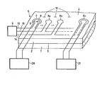
- The Figure diagrammatically shows a bubble domain device.
- Films of the nominal composition {Gd,Y }3 (Fe,Mn,Ga)5O12 were grown on a first series of GGG substrates by liquid phase epitaxy methods from a melt while using a PbO/B2O3 flux. The Ga content was varied to adjust the saturation magnetization, the ratio Gd2O3/Y2O3 in the melt was varied to vary the lattice constant of the deposited layer, and the Mn content was varied to adapt the magneto-elastic constant. While using a PbO/B2O3 melt, films of the nominal composition {Bi,Y}3 (Fe,Mn,Ga)5012 were also deposited on a second series of GGG substrates.
- The layers were grown on substrates which were dipped horizontally in the melt and had a diameter of 2.5 cm and a (100) oriented deposition face at temperatures between 750 and 950°C for periods which varied from 0.25 - 2 minutes, the substrates being rotated at 100 rpm, while after every 5 revolutions the direction of rotation was reversed. The film thicknesses varied from 0.5 to 4.5 /um.
- For the growth of a layer of the nominal composition {Gd,Y}3 (Fe,Mn,Ga)5O12, the following oxides were weighed out in the following quantities:

- The mixture was melted and heated at a temperature of 876°C. A Gd3Ga5O12 substrate having a (100) oriented deposition face was dipped in the melt for 2 minutes, resulting in the deposition of a layer of 4.4 /um thickness.
- Estimated composition of the layer:Y1.1,Gd1.9Fe3.8,Mn0.7 , Ga0.5, O12.
- For the growth of a layer of the nominal composition {Y,Gd}3(Fe,Mn)5O12, the following oxides were weighed out in the following quantities:

- The mixture was melted and heated at a temperature of 876°C. A Gd3Ga5O12 substrate having a (100) oriented deposition face was dipped in the melt for 15 seconds resulting in the deposition of a 0.55 /um thick layer.
- Estimated composition of the layer:Y1.1, Gd1.9,Fe3.8, Mn l.2' O12.
- For the growth of a layer of the nominal composition {Y, Gd}3(Fe,Mn, Ga)5O12, the following oxides were weighed out in the following quantities:

- The mixture was melted and heated at a temperature of 898°C. A Gd3Ga5O12 substrate having a (100) oriented deposition face was dipped in the melt for 2 minutes of 3.88 µm. Estimated composition of the layer:
- Y2.1, Gd0.9, Fe 3.8' Mn0.7, Ga0.5, O12.
- For the growth of a layer of the nominal composition {Hi,Y}3(Fe,Mn,Ga)5O12, the following materials were weighed out in the following quantities:

- The mixture was melted and heated at a temperature of 778°C. A Gd3Ga5O12 substrate having a (100) oriented deposition face was dipped in the melt for 60 seconds resulting in the deposition of a layer having a thickness of 0.76 µm.
- The Table below gives the properties of the magnetic layers grown by the processes described in Examples 1 to 4 above.

- In the above Table, B is the stable strip domain width, Ku is the uniaxial anisotropy constant,ΔH is the ferromagnetic resonance line width at 10 GH , 4 π Ms is the saturation magnetization, /u is the bubble domain mobility and Q = HA/4 πM, where HA is the anisotropy field and 4 π M is the demagnetizing field, which denotes values which have not been measured directly but calculated on the basis of other, measured, values.
- The uniaxial anisotropy constants of the resulting films were determined by means of a torsion magnetometer. Values up to 2x10 erg/cm3 were thus realized for both {Gd,Y}3(Fe,Mn)5O12 and (Bi,Y)3(Fe,Mn,Ga)5O12 films on GGG.
- Herewith a new type of bubble domain material has been provided with, also as regards saturation magnetization and mobility, properties which make it excellently suitable for use in bubble domain propagation devices with submicron bubble domains. (Materials with 0.4 /um diameter bubble domains have been realized). Those skilled in the art will be capable of varying the composition of the bubble domain layer while using the above given general composition and without departing from the scope of this invention. The examples are therefore only by way of illustration and are not limiting.
- In an embodiment to the invention a substrate 1 and a
bubble domain layer 2 for the active storage and movements of magnetic domains are used, have acommon interface 3, each being characterized by a special nature and by an above-described mutual relation. Thelayer 2 has anupper surface 4 remote from theinterface 3, thesurface 4 bearing certain conventional elements for the excitation propagation and sensing of magnetic domains. Thelayer 2 for storing or moving magnetic domains may, generally speaking, be the place of each of the various processes for digital logics as described elaborately in Patent Specifications and other technical literature. Reference may be made, for example, to the Bell System Technical Journal, XLVI, No. 8, 1901 - 1925 (1967) which comprises an article entitled "Properties and Device Applications of Magnetic Domains in Orthoferrites". - The Figure of the accompanying drawing shows a rather simple configuration which only represents a fragment of a normally larger construction comprising a
layer 2 for storage and movement of magnetic domains and various conventional elements for the excitation, propagation and sensing of magnetic domains. The figure may be considered to be ashift register 5 in which according to the invention alayer 2 is used of a magnetic material having a high uniaxial magnetic anisotropy and a high domain mobility. The easy axis of magnetisation of thelayer 2 is perpendicular to thesurface 4. The general magnetization condition oflayer 2 is represented by lines of magnetic flux perpendicular to thesurface 4. Magnetic flux lines situated within the domains and directed opposite to their surroundings are shown by plus signs, for example theplus sign 6 withinloop 7. -
Conductors domain propagator 9, can be connected to or be present in the immediate proximity of thesurface 4 of thelayer 2. Theconductors example loops - During operation of the device the magnetic domains are generated by means of a
conventional domain generator 20 combined with aloop 7 which is substantially coaxial with aloop 8. A stable cylindrical magnetic domain, for example, the position of the domain indicated by theplus sign 6, can be propagated in incremental steps from the place of theloop 8 to the place of theloop 8a, then to that of theloop 8b, etc. by successive excitation of theconductors domain propagator 9. When a propagated magnetic domain reachesloop 8n, it can be detected by means ofdomain sensor 21. It will be obvious that other digital logic functions can easily be carried out while using the same known methods as those which are used in the example of theshift register 5.
Claims (7)
Applications Claiming Priority (2)
| Application Number | Priority Date | Filing Date | Title |
|---|---|---|---|
| NL8004201 | 1980-07-22 | ||
| NL8004201A NL8004201A (en) | 1980-07-22 | 1980-07-22 | Apparatus for the advancement of magnetic domains. |
Publications (3)
| Publication Number | Publication Date |
|---|---|
| EP0044586A2 true EP0044586A2 (en) | 1982-01-27 |
| EP0044586A3 EP0044586A3 (en) | 1982-02-03 |
| EP0044586B1 EP0044586B1 (en) | 1984-08-01 |
Family
ID=19835654
Family Applications (1)
| Application Number | Title | Priority Date | Filing Date |
|---|---|---|---|
| EP81200763A Expired EP0044586B1 (en) | 1980-07-22 | 1981-07-03 | Device for propagating magnetic domains |
Country Status (5)
| Country | Link |
|---|---|
| US (1) | US4435484A (en) |
| EP (1) | EP0044586B1 (en) |
| JP (2) | JPS5752113A (en) |
| DE (1) | DE3165225D1 (en) |
| NL (1) | NL8004201A (en) |
Cited By (1)
| Publication number | Priority date | Publication date | Assignee | Title |
|---|---|---|---|---|
| EP0166924A2 (en) * | 1984-07-02 | 1986-01-08 | Allied Corporation | Faceted magneto-optical garnet layer |
Families Citing this family (8)
| Publication number | Priority date | Publication date | Assignee | Title |
|---|---|---|---|---|
| JPS5972707A (en) * | 1982-10-20 | 1984-04-24 | Hitachi Ltd | Garnet film for magnetic bubble element |
| US4584237A (en) * | 1983-04-04 | 1986-04-22 | Litton Systems, Inc. | Multilayer magneto-optic device |
| US4728178A (en) * | 1984-07-02 | 1988-03-01 | Allied Corporation | Faceted magneto-optical garnet layer and light modulator using the same |
| FR2572844B1 (en) * | 1984-11-02 | 1986-12-26 | Commissariat Energie Atomique | MAGNETIC MATERIAL OF THE GRENATE TYPE, MAGNETIC FILM WITH HIGH ROTATION FARADAY COMPRISING SUCH A MATERIAL AND METHOD FOR MANUFACTURING THE SAME |
| JPH0653267B2 (en) * | 1985-11-15 | 1994-07-20 | トヨタ自動車株式会社 | Resin coating method for metal parts |
| US5021302A (en) * | 1986-08-15 | 1991-06-04 | At&T Bell Laboratories | Bismuth-iron garnets with large growth-induced magnetic anisotropy |
| JPH0354198A (en) * | 1989-07-20 | 1991-03-08 | Shin Etsu Chem Co Ltd | Oxide garnet single crystal |
| JP2904668B2 (en) * | 1993-02-10 | 1999-06-14 | 信越化学工業株式会社 | Garnet magnetic oxide single crystal for magnetostatic wave device, method for producing the same, and magnetostatic wave device |
Citations (3)
| Publication number | Priority date | Publication date | Assignee | Title |
|---|---|---|---|---|
| DE2232902A1 (en) * | 1971-08-04 | 1973-02-15 | Ibm | MAGNETIC GARNET SINGLE CRYSTAL LAYER |
| DE2431419A1 (en) * | 1973-07-02 | 1975-01-23 | Rockwell International Corp | COMPOSITE MATERIAL IN WHICH MAGNETIC BLADDER DOMAAS CAN BE CREATED, WHICH HARD BLADDER DOMAAS ARE SUPPRESSED |
| US4138530A (en) * | 1977-01-17 | 1979-02-06 | U.S. Philips Corporation | Magnetic structures |
Family Cites Families (3)
| Publication number | Priority date | Publication date | Assignee | Title |
|---|---|---|---|---|
| US3745046A (en) | 1970-12-28 | 1973-07-10 | North American Rockwell | Method for producing bubble domains in magnetic film-substrate structures |
| JPS4929497A (en) * | 1972-07-18 | 1974-03-15 | ||
| US4018692A (en) | 1973-10-04 | 1977-04-19 | Rca Corporation | Composition for making garnet films for improved magnetic bubble devices |
-
1980
- 1980-07-22 NL NL8004201A patent/NL8004201A/en not_active Application Discontinuation
-
1981
- 1981-06-18 US US06/274,974 patent/US4435484A/en not_active Expired - Fee Related
- 1981-07-03 DE DE8181200763T patent/DE3165225D1/en not_active Expired
- 1981-07-03 EP EP81200763A patent/EP0044586B1/en not_active Expired
- 1981-07-20 JP JP56112382A patent/JPS5752113A/en active Pending
-
1987
- 1987-05-25 JP JP1987077433U patent/JPH0219932Y2/ja not_active Expired
Patent Citations (3)
| Publication number | Priority date | Publication date | Assignee | Title |
|---|---|---|---|---|
| DE2232902A1 (en) * | 1971-08-04 | 1973-02-15 | Ibm | MAGNETIC GARNET SINGLE CRYSTAL LAYER |
| DE2431419A1 (en) * | 1973-07-02 | 1975-01-23 | Rockwell International Corp | COMPOSITE MATERIAL IN WHICH MAGNETIC BLADDER DOMAAS CAN BE CREATED, WHICH HARD BLADDER DOMAAS ARE SUPPRESSED |
| US4138530A (en) * | 1977-01-17 | 1979-02-06 | U.S. Philips Corporation | Magnetic structures |
Non-Patent Citations (2)
| Title |
|---|
| IEEE Transactions on Magnetics, Vol. MAG 10, No. 3, September 1974, G. DIONNE "Stress Effects on Remanence Ratios from Changes in Spike Domain Volume" pages 947-949. * |
| Journal of Applied Physics, Vol. 51, No. 5, May 1980, New York, US D. BREED et al. "Fast Wall Motion in Garnet Films with Orthorhombic Anisotropy" pages 2780-2783 * |
Cited By (2)
| Publication number | Priority date | Publication date | Assignee | Title |
|---|---|---|---|---|
| EP0166924A2 (en) * | 1984-07-02 | 1986-01-08 | Allied Corporation | Faceted magneto-optical garnet layer |
| EP0166924A3 (en) * | 1984-07-02 | 1987-02-04 | Allied Corporation | Faceted magneto-optical garnet layer |
Also Published As
| Publication number | Publication date |
|---|---|
| EP0044586B1 (en) | 1984-08-01 |
| JPH0219932Y2 (en) | 1990-05-31 |
| DE3165225D1 (en) | 1984-09-06 |
| NL8004201A (en) | 1982-02-16 |
| JPS5752113A (en) | 1982-03-27 |
| US4435484A (en) | 1984-03-06 |
| EP0044586A3 (en) | 1982-02-03 |
| JPS62197817U (en) | 1987-12-16 |
Similar Documents
| Publication | Publication Date | Title |
|---|---|---|
| US4263374A (en) | Temperature-stabilized low-loss ferrite films | |
| EP0044586B1 (en) | Device for propagating magnetic domains | |
| Giess et al. | Rare earth-yttrium iron-gallium garnet epitaxial films for magnetic bubble domain applications | |
| JP3198053B2 (en) | Products made of magneto-optical material with low magnetic moment | |
| US4563236A (en) | Method for making large area stable domains | |
| EP0044109B1 (en) | Device for propagating magnetic domains | |
| US5898516A (en) | Faraday rotator having a rectangular shaped hysteresis | |
| Van Uitert et al. | Control of bubble domain properties in garnets | |
| US4647514A (en) | Magnetic domain device having a wide operational temperature range | |
| US5608570A (en) | Article comprising a magneto-optic material having low magnetic moment | |
| US4138530A (en) | Magnetic structures | |
| US6733587B2 (en) | Process for fabricating an article comprising a magneto-optic garnet material | |
| JPH07104225A (en) | Faraday rotator | |
| US4169189A (en) | Magnetic structure | |
| JPH09186016A (en) | Product containing exchange coupled magnetic material | |
| US4698281A (en) | Garnet-type magnetic material high faraday rotation magnetic film containing such a material and process for the production thereof | |
| US4269651A (en) | Process for preparing temperature-stabilized low-loss ferrite films | |
| US4001793A (en) | Magnetic bubble domain composite with hard bubble suppression | |
| US5021302A (en) | Bismuth-iron garnets with large growth-induced magnetic anisotropy | |
| Giess et al. | Gallium concentration effects on magnetic bubble films of EuTm2 (Fe, Ga) 5O112 garnet grown by liquid phase epitaxy | |
| Moody et al. | Properties of Gd y Y 3-y Fe 5-x Ga x O 12 films grown by liquid phase epitaxy | |
| JPS59122B2 (en) | How to deposit a layer of bubble domain material onto a single crystal substrate | |
| US4468438A (en) | Garnet epitaxial films with high Curie temperatures | |
| EP1418597A1 (en) | Method for producing ferromagnetic garnet material, garnet material and its use | |
| Gyorgy | The Imperfect Solid—Magnetic Properties |
Legal Events
| Date | Code | Title | Description |
|---|---|---|---|
| PUAI | Public reference made under article 153(3) epc to a published international application that has entered the european phase |
Free format text: ORIGINAL CODE: 0009012 |
|
| PUAL | Search report despatched |
Free format text: ORIGINAL CODE: 0009013 |
|
| AK | Designated contracting states |
Designated state(s): DE FR GB IT NL SE |
|
| AK | Designated contracting states |
Designated state(s): DE FR GB IT NL SE |
|
| 17P | Request for examination filed |
Effective date: 19820402 |
|
| RAP1 | Party data changed (applicant data changed or rights of an application transferred) |
Owner name: N.V. PHILIPS' GLOEILAMPENFABRIEKEN |
|
| ITF | It: translation for a ep patent filed |
Owner name: ING. C. GREGORJ S.P.A. |
|
| GRAA | (expected) grant |
Free format text: ORIGINAL CODE: 0009210 |
|
| AK | Designated contracting states |
Designated state(s): DE FR GB IT NL SE |
|
| REF | Corresponds to: |
Ref document number: 3165225 Country of ref document: DE Date of ref document: 19840906 |
|
| ET | Fr: translation filed | ||
| PLBE | No opposition filed within time limit |
Free format text: ORIGINAL CODE: 0009261 |
|
| STAA | Information on the status of an ep patent application or granted ep patent |
Free format text: STATUS: NO OPPOSITION FILED WITHIN TIME LIMIT |
|
| 26N | No opposition filed | ||
| PG25 | Lapsed in a contracting state [announced via postgrant information from national office to epo] |
Ref country code: NL Effective date: 19860201 |
|
| NLV4 | Nl: lapsed or anulled due to non-payment of the annual fee | ||
| PGFP | Annual fee paid to national office [announced via postgrant information from national office to epo] |
Ref country code: GB Payment date: 19900702 Year of fee payment: 10 |
|
| PGFP | Annual fee paid to national office [announced via postgrant information from national office to epo] |
Ref country code: SE Payment date: 19900726 Year of fee payment: 10 |
|
| PGFP | Annual fee paid to national office [announced via postgrant information from national office to epo] |
Ref country code: DE Payment date: 19900921 Year of fee payment: 10 |
|
| PG25 | Lapsed in a contracting state [announced via postgrant information from national office to epo] |
Ref country code: GB Effective date: 19910703 |
|
| PG25 | Lapsed in a contracting state [announced via postgrant information from national office to epo] |
Ref country code: SE Effective date: 19910704 |
|
| GBPC | Gb: european patent ceased through non-payment of renewal fee | ||
| PG25 | Lapsed in a contracting state [announced via postgrant information from national office to epo] |
Ref country code: DE Effective date: 19920401 |
|
| PGFP | Annual fee paid to national office [announced via postgrant information from national office to epo] |
Ref country code: FR Payment date: 19930728 Year of fee payment: 13 |
|
| EUG | Se: european patent has lapsed |
Ref document number: 81200763.1 Effective date: 19920210 |
|
| PG25 | Lapsed in a contracting state [announced via postgrant information from national office to epo] |
Ref country code: FR Effective date: 19950331 |
|
| REG | Reference to a national code |
Ref country code: FR Ref legal event code: ST |